Note: Descriptions are shown in the official language in which they were submitted.
.~
215722~
.
-- 1 --
METHOD AND APPARATUS FOR FLUXING AND SOLDERING
TERMINALS ON A PRINTED CIRCUIT soARD
This invention relates to methods and apparatus
for fluxing and soldering terminals on a printed circuit
board.
In the manufacture of printed circuit boards in
which soldering at terminals positions on the boards is
performed by known wave soldering techniques in an in-line
process, soldering flux is sprayed onto the boards'
0 undersurfaces in a fluxing station, the boards then
proceeding through at least one preheating station before
being subjected to the solder wave. Quality control of
such a process is essential not only to maintain required
competitive quality of the final product, but also to
m;n;m;ze wastage which may be extremely expensive to the
board manufacturer. It is known with any particular
fluxing and soldering apparatus, any fluxing or soldering
variation which develops is inclined to be repetitive.
Hence, after development of the variation, all boards made
by the apparatus will have similar specific defects which
will not be corrected on further boards until the variation
in the process has been corrected. The design and
operation of the apparatus may be such that some
operational variation may not cause products to be
commercially acceptable, but in other cases operational
variation will more certainly cause failure to obtain
commercial acceptance. Failure may be caused by control in
application of flux onto the surface of a board, i.e. too
littlé or too much flux applied in certain areas, which may
have an effect on the final soldering operation or upon the
surface insulation resistance (SIR) of the finished circuit
board. This is particularly the case in the use of a wave
soldering operation in printed circuit board manufacture in
which flux is applied to boards moving in an upwardly
inclined direction in series towards a wave soldering
station. An attempt is made generally to influence the
quantity of flux applied to each particular board, but in
21~72,2~
.
-- 2
being transported into the wave soldering station, and
dependent upon the orientation of each board, flux
distribution may change.
The present invention seeks to provide a method
and apparatus for fluxing and soldering terminals on a
printed circuit board in which the above problems are
minimized.
Accordingly, the present invention provides
according to one aspect, a method of fluxing and soldering
o terminals on a printed circuit board comprising:- moving
the printed circuit board along a passline through a flux
application station; directing a wall of flux across a
surface of the board as it moves through the flux
application station while decreasing in controlled manner
the flow rate of the flux directed at the board surface
until the board has passed completely through the wall of
flux whereby the thickness of flux upon the board surface
decreases from a leading end to a trailing end of the
board; moving the printed circuit board out of the flux
application station and in an upwardly inclined manner
towards a solder application station thereby causing the
flux to flow towards the trailing end of the board and
redistribute the flux towards providing a constant flux
thickness over the board; and then moving the board through
the solder application station to apply solder to the
terminals.
It has been found that with conventional methods,
flux applied to a printed circuit board surface in a wave
soldering process tends to flow`downwardly on the surface
towards the trailing end of the board as the board is moved
towards the solder application station. This may produce
less flux than is required at the leading end of the board,
an increase in flux towards the trailing end and perhaps
more flux than is needed at the trailing end. Because of
the lack of uniformity in flux application, soldered joints
may not be up to the required standard and in the case of
~no clean' fluxes used more recéntly, problems concerning
`- 21~7225
-- 3
surface insuIation resistance of a printed circuit board
may result. In use of the method according to the
invention defined above, reduction in the flow rate of the
flux from the leading to the trailing end of the board
serves to counteract this tendency. As a result, and
taking into account the tendency of flux flow towards the
trailing end of the board, the desired maximum flow rate
essentially should apply more flux than is actually
required at the leading end and the desired m;n;mllm flow
o rate essentially should apply less than is required at the
trailing end. Preferably, the flux flow rate is decreased
progressively from its desired maximum to its desired
m; n; m~]m, but alternatively incremental steps in flow rate
reduction are also advantageous.
The invention also includes a method of fluxing
and soldering terminals on a plurality of printed circuit
boards moving in series along a passline through a flux
application station and then through a solder application
station, the method comprising:- directing a wall of flux
across a surface of each board in turn as it moves through
the flux application station with a leading end of the
printed circuit board moving into the wall of flux so that
the wall of flux is directed along the printed circuit
board from its leading end to a trailing end of the board
and while simultaneously decreasing in controlled manner,
from a desired maximum, the flow rate of the flux, being
applied to the board whereby the thickness of flux upon the
board surface decreases from its leading end to the
trailing end of the board; moving each board out of the
flux application station and, to complete a flux flow rate
cycle, increasing the flow rate of the flux to a desired
maximum after each board is moved out of and before the
leading end of the next succeeding board moves into the
flux application station; after each board has moved out of
the flux application station, moving the board in an
upwardly inclined manner towards a solder application
station thereby causing flux to flow towards the trailing
2157225
-- 4
end of the board to redistribute the flux towards providing
a constant flux thickness over the board; and then moving
the board through the solder application station to apply
solder to the terminals.
The flow of flux may be controlled to operate in
various ways. The rate of flow of flux may be decreased to
a m;n;ml]m which is maintained until a next succeeding board
approaches the flux application station, the flux flow then
being increased to its maximum. Alternatively, after the
o passage of each board through the flux application station,
the flow of flux may be reduced to zero pending the
approach of a succeeding board towards the flux application
station. with the use of the latter method, there may be a
saving in flux lost in being dissipated from the wall when
directed at a space between two boards in the series and
also in the case where a succeeding board is a substantial
distance behind the previous board.
Ideally, to control the process each printed
circuit board, as it approaches the flux application
station, is sensed by a sensing means and the sensing means
controls the flow rate of the flux into the wall so as to
increase the flow rate to its desired maximum before the
leading end of the printed circuit board reaches the flux
application station.
In addition, the invention also includes a wave
soldering apparatus comprising:- a flux application
station and a solder application station disposed
downstream of the flux application station along a passline
for printed circuit boards to be passed through the
30 apparatus; means for creating a wall of flux in the flux
application station and for directing it upwardly towards
the passline to coat, with flux, printed circuit boards as
they move through the flux application station; and means
for controlling the flow rate of the flux into the wall
whereby the flow rate decreases from a desired maximum as
the leading end of a printed circuit board enters the wall
until the board has passed completely through the wall.
2157225
-- 5
Embodiments of the invention will now be
described, by way of example, with reference to the
accompanying drawings, in which:-
Figure 1, relating to a first embodiment, is a
diagrammatic side elevational view of a wave solderingapparatus showing printed circuit boards being fed
therethrough;
Figure 2 is a diagrammatic view partly in cross-
section along line II-II in Figure 1 of part of the
lo apparatus of the first embodiment;
Figure 3 is a graph showing the control of flux
application to printed circuit boards being fed through the
apparatus;
Figure 4 is a view similar to Figure 1 of a second
embodiment;
Figure 5 is a plan view of a monitoring means of
the second embodiment and to a larger scale than Figure 4;
Figure 6 is a view similar to Figure 2 of the
second embodiment; and
Figure 7 is a view similar to Figure 3 of the
second embodiment.
In the embodiment as shown in Figure 1, a wave
soldering apparatus 10 is basically of conventional
construction in that it has an inclined conveyor 12 moving
upwards from left to right in the Figure for conveying
printed circuit boards 14 through a flux application
station 16, past preheaters 18, and then through a wave
soldering application station 20.
In addition, the apparatus comprises a means 21
for creating a wall of flux in the flux application and for
directing the flux upwardly against an undersurface of each
board as it moves along the conveyor 12. The means 21
comprises a conventional rotary perforate drum 22 entering
into a bath 24 so as to be partially submerged in flux
material 26 contained in the bath. In practice, with the
printed circuit boards fed in series along the conveyor 12,
the drum 22 is rotated and with pressurized air being fed
21 j7225
.
-- 6
into the drum, flux material contained upon the drum is
driven from the drum in an upward direction by the
pressurized air issuing through the perforations to create
the wall 28 of flux as shown diagrammatically in Figure 1.
The apparatus 10 of the first embodiment differs
from the conventional apparatus in that it has, in
accordance with the invention, means for controlling the
rate of flow of the flux into the wall. The control for
the flow rate enables the flow rate to decrease from a
lo desired maximum as the leading end of a printed circuit
board enters the wall until the board has passed completely
through the wall. The control means comprises a sensor for
sensing when the leading end of each board gets to a
certain position as it approaches the flux application
station so as to enable the flux to be turned up to its
maximum rate of flow preparatory to the leading end
reaching that station. As shown in Figures 1 and 2 the
sensor comprises an optical sensor 30 which sends a signal
to a computer 32 upon being triggered by the leading end of
a board 14. The drum 12 is rotated at its two ends by
gears 33 driven by motors 34. The computer controls the
operation of each motor 34 through a potentiostat 35. Upon
receiving the signal from sensor 30, the computer then
operates the two potentiostats simultaneously so as to
increase drum rotation to a maximum consistent with a
desired maximum flow rate of the flux in the wall at the
position to be occupied by the undersurface of the printed
circuit board as it passes through the flux application
station. The computer then operates through the
30 potentiostats to ensure that the motors 34 drive the drum
12 at a progressively decreasing speed whereby the flow
rate of the flux into the wall 28 at the location of the
board undersurface also decreases in a desired manner.
This decrease in flow rate continues until at least the
35 trailing edge of a printed circuit board has passed
outwardly beyond the wall so that the whole of the board
has now been coated with flux on its under surface. In
21~722~
-
-- 7
conventional manner the drum 12 is fed with compressed air
from an air knife 37 in the drum supplied by an air pipe
36.
In operation of the apparatus of the first
embodiment and with reference to Figures 1 and 2 and also
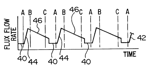
particularly to Figure 3, at commencement of operations the
solder wave at a solder application station 38 downstream
from the flux application station, is already operational
as is the wall 28 of flux. Before any printed circuit
lo board reaches the flux application station the flow rate of
the flux into the wall at a position for contacting the
undersurface of a board is shown at the lower position 40
of the graph 42 in Figure 3, i.e. with the drum 12 being
rotated at its lowest desired ro~ational speed. Figure 3
shows a series of cycles in the flow rate of the flux into
the effective part of the wall which will contact the
undersurface of each board. The flow rate is constant as
indicated by the part of the graph 40 until a first board
has its leading end advanced to such a position that the
sensor 30 is operated. This is shown by the left-hand
station ~A' in Figure 3. A signal sent from the sensor 30
then instructs the computer 32 to increase the drive speeds
of the motors 34 to rotate the drum 12 at its maximum
desired speed at which point the flow rate rapidly
increases as shown by the upward portion 44 of the graph at
the left-hand side of Figure 3, to a maximum flow rate in
the wall at the point of contact with the printed circuit
board. The board then progresses through the flux
application station during which time the potentiostats 35
are controlled by the computer 32 to progressively decrease
the rotational speeds of the motors 34 and thus of the drum
12 in desired manner. The flux flow application rate to
the board undersurface then decreases in desired manner as
shown by graph portion 46. It should be noted that the
leading end of the board enters the wall (position B on the
graph) after controlled decrease in rotational speed of
drum 12 has commenced. When the trailing end has passed
21S722~
-
-- 8
the flux application station (position C in Figure 3) the
flux flow rate continues to decrease as shown by graph
portion 46 for a m;n;ml]m period during controlled
progressive rotational speed of the drum 12. The drum
speed is then decreased rapidly to provide a rapid decrease
in flux flow rate to a second position 40 corresponding to
the first position. A succeeding printed circuit board
having its leading end operating the sensor (next position
A in Figure 3) then effectively causes the drum to rotate
o again at its maximum desired speed in order to start a
repeat in the flux flow cycle. The cycles are repeated for
each board as it passes into and out of the flux
application station.
As will be seen from the above description,
because the flux is applied in the manner described with a
progressive reduction in flux in the wall at the position
of application of the flux onto each board, then
necessarily the amount of flux applied to the undersurface
of the board decreases progressively from the leading end
20 to the trailing end. However, as each printed circuit
board proceeds upwardly along the conveyor 12 towards the
solder application station, the flux will flow downwardly
along the inclined undersurface of the board so that the
flux at the upper end portions decreases in thickness and
25 that at the lower end portions increases in thickness.
There is a tendency therefore for the flux thickness over
the whole board to change towards a constant thickness from
one end of the board to the other. Bearing this in mind,
and knowing the speed and inclination of the conveyor 12
and the characteristics of flow of the flux, a
determination may be made on how to control the reduction
in flow rate of the flux whereby a substantially constant
thickness of flux may be obtained from end to end of the
board by the time it reaches the solder application
35 station. It follows therefore than in using the flow
control described in the embodiment and according to the
invention, upon each printed circuit board reaching the
21572~5
-
g
solder application station, the flux on the board is of
substantially constant thickness all over the undersurface
of the printed circuit board and this thickness is as
required for most efficient solder application at the
terminal positions.
As may be seen therefore ~rom the first embodiment
and falling within the scope of the invention, it is
possible to control the thickness of the flux over the
whole board area to that which is required upon that board
0 and this process will reduce any tendency for poor quality
solder application at the terminal positions. Hence, there
is a m;n;m;zed possibility of any boards not meeting the
required quality standards and this results in less
percentage scrap in commercial use of the process.
In a second embodiment now to be described, a wave
soldering apparatus 100 is constructed similarly to the
apparatus 10 of the first embodiment and has the same
advantages. In addition, however, and as will become
apparent, the apparatus of the second embodiment is capable
20 of correcting any deviation of the flow rate of flux away
from its desired flow rate at any instant.
In the second embodiment in which parts similar to
those in the first embodiment bear the same reference
numerals, the apparatus 100 has a monitoring means,
designated generally at 102 in Figure 4, for monitoring the
application of flux directed onto printed circuit boards 14
moving along the conveyor 12. The monitoring means, as is
more clearly shown in Figure 5, comprises a rigid
rectangular frame 104 defining an opening 106 disposed
above the drum 22. The opening 106 is provided for
enabling the wall 28 of flux to pass through the opening in
order to reach the undersides of the printed circuit
boards. The frame 104 provides a means for supporting a
means for transmitting and receiving infra red light.
The means for transmitting infrared light
comprises a fiber optic launch and lens assembly 108 (for
instance as made by Terra Hertz Inc, of Oriskiny, New York)
2 1 s 7 2 25
_
- 10 -
the assembly 108 being located in a fixed position on a
beam 110 of the frame 104, the beam 110 extending
transversely of the passline for the conveyor 12. The
position of the conveyor is shown in Figure 5 by the chain-
dotted conveyor edges. The launch assembly 108 is orientedto direct light rearwardly through the wall of flux, i.e.
across the opening 106. The means for receiving the
infrared light which has past through the wall of flux and
is unabsorbed thereby comprises a receiving assembly 112
0 which is similar to the launch assembly 108 and is disposed
upon another beam 110 on the other side of the opening 106.
The assembly 108 is positioned such that it is located with
its lens 114 accurately aligned with a lens 116 of the
assembly 112. The lens 114 is a focusing lens for focusing
the light at a position midway through the wall of flux
between the two beams 110, the unabsorbed light then being
divergent as it extends towards the corresponding lens 116
on the other side of the wall. The focused light is
indicated by reference 118 in Figure 5. The monitoring
means also includes an optic cable 120 for transmitting the
infrared light to the assembly 108 and another cable 122
for receiving the light from the assembly 112 on the other
beam 110. Only certain optical fiber cables are
manufactured which may be used at the present time for
transmitting infrared light signals. Such cables
incorporate zinc fluoride fibers and are made by Terra
Hertz Inc. (referred to above) or alternatively by Galileo
Fiber Optics.
As shown by Figure 6, the optical fiber cable 120
from the assembly 108 commences at a source 124 of infrared
light. Signals received by the other assembly 112 are
transmitted by cable 122 to the computer 32. In use,
signals are sent by the receiving assembly 112 to computer
32 and which indicate the quantity of flux in the wall 28
at a position slightly below the positions of printed
circuit boards 14 passing along the conveyor 12. If any of
these signals indicates that the flux density at any
215722~
_,
-- 11 --
specific time is below that which is desired for that
specific time, then the computer adjusts the speed of
motors 34 to rotate the drum 22 at the required speed to
adjust the flow rate. Thus, where the actual flow rate as
shown in chain-dotted outline 123 in Figure 7 is not that
which is desired, (the desired rate being in full outline
in Figure 7), the flow rate is adjusted so as to move the
actual flow rate to the desired rate. This is shown, for
instance, by the merging of the chain-dot outline at
o positions 124 on the curve in Figure 7. An accurate
control is thus provided for the flow rate of the flux in
the second embodiment.