Note: Descriptions are shown in the official language in which they were submitted.
2157259
AN ELECTRONIC DEVICE ASSEMBLY AND
A MANUFACTURING METHOD OF THE SAME
BACKGROUND OF THE INVENTION
The present invention relates to an electronic device
assembly, and more particularly to an electronic device assembly
including a f first substrate and a second substrate mounted on the
first substrate.
An example of a conventional electronic device is disclosed
in U.S.P. 5,203,075.
Referring to Fig. 10 of the above reference, a semiconductor
device 43 is mounted on a flexible substrate 31. The flexible
substrate 31 is connected to a substrate 13 via solder.
Referring to Figs . 6 and 9 of the reference, a solder member
32 and a solder paste 27 connect the flexible substrate 31 and
the substrate 13. Part of the solder member 32 is positioned in
a through-hole provided in the flexible substrate 31.
The aforementioned structure has the following problems.
First, the solder connection is susceptible to failure
because it is not protected from mechanical stress.
Specifically, the solder connection is apt to fall off, be
broken, or be short circuited with the adjacent solder
connection. This problem becomes serious when a relatively heavy
device such as a heat sink is mounted on the flexible substrate.
The failure of the solder connection is also caused by thermal
cycling (i.e., repetitive heating and cooling).
Second, the solder is further susceptible to failure because
it is not protected from air humidity (e.g., the moisture in the
air).
-1-
2157259
Third, it is difficult to control the gap precisely between
the flexible substrate 31 and the substrate 13 because it is
difficult to keep the flexible substrate 31 flat. If the gap
between the flexible substrate 31 and the substrate 13 is uneven,
the reliability of the solder connection decreases.
SUMMARY OF THE INVENTION
In view of the aforementioned problems, one object of the
present invention is to enhance the reliability of the connection
between substrates. Specifically, the connection is protected
from mechanical stress, stress due to thermal cycling, and air
humidity.
Another object of the present invention is to easily control
the gap between the substrates.
According to the present invention, an electronic device
assembly includes a first substrate, a second substrate, a
connecting member, and a resin. The first substrate has a first
surface, a second surface and a connecting structure on the
second surface. The second substrate has a first surface, a
second surface and a first pad formed on the second surface. The
first pad faces the connecting structure of the first substrate.
The connecting member is interposed between the first and second
substrates and connects the connecting structure and the first
pad. The resin is provided between the first and second
substrates. The first substrate is attached to the second
substrate by the resin.
The connecting member may include solder. The connecting 1
structure may include a through-hole provided in the first
substrate. At least a part of the solder may be positioned in
-2-
2157259
the through-hole.
The connecting member may include a film and a conductive
body provided in the film. The conductive body is interposed
between and connects the first pad and the connecting structure.
The resin fills an area between the first substrate and the film
and an area between the film and the second substrate.
The connecting structure may include a second pad provided
on the second surface of the first substrate. The connecting
member may include an anisotropic conductive sheet connecting the
first and second pads. The resin fills an area between the first
substrate and the anisotropic conductive sheet and an area
between the anisotropic conductive sheet and the second
substrate.
According to the present invention, the electronic device
assembly may be manufactured by the following process. In a
first step, the first substrate is prepared. In the second step,
the second substrate is prepared. In a third step, solder is
provided on the first pad. In a fourth step, the first substrate
is positioned so that the connecting structure is positioned on
the solder. In a fifth step, a resin is prepared between the
first and second substrate. In a sixth step, the solder and the
resin are heated simultaneously. The solder melts to connect the
first pad and the connecting structure. The resin is set to
couple the first substrate to the second substrate.
The process may include a step of confirming whether at
least a portion of the solder protrudes from the through-hole of
the first substrate.
The electronic device assembly may also be manufactured by
-3-
2157259
the following process. In a first step, the first substrate is
prepared. In a second step, the second substrate is prepared.
In a third step, solder is prepared on the first pad. In a
fourth step, the resin is positioned on the first surface of the
second substrate. In a fifth step, the first substrate is
positioned so that the connecting structure is positioned on the
solder. In a sixth step, the solder and the resin are heated
simultaneously. The solder is melted to connect the first pad
and the connecting structure. The resin is set to couple the
first substrate to the second substrate.
The electronic device assembly also may be manufactured by
the following process. In a first step, the first substrate is
prepared. In a second step, the second substrate is prepared.
In a third step, a connecting member is prepared. The connecting
member includes a film having first and second surfaces and a
conductive body provided in the film. The first and second
portions of the conductive body protrudes from the first and
second surfaces of the film, respectively. In a fourth step, the
connecting member is positioned so that the second portion of the
conductive body is positioned on the first pad of the second
substrate. In a fifth step, the first substrate is positioned
so that the connecting structure is positioned on the first
portion of the conductive body. In a sixth step, the first pad
is connected to the second portion of the conductive body. The
first portion of the conductive body is connected to the
connecting structure. In a seventh step, a resin is prepared
between the first substrate and the film and between the film and
the second substrate. In a eighth step, the resin is set.
-4-
2157259
The electronic device assembly may be manufactured
by the following process. In a first step, the first
substrate is prepared. In a second step, the second substrate
is prepared. In a third step, an anisotropic conductive sheet
is positioned on the second pad of the second substrate. In a
third step, the first substrate is positioned on the
anisotropic conductive sheet so that the first pad faces the
second pad via the anisotropic conductive sheet. In a fourth
step, a resin is provided between the first substrate and the
anisotropic conductive sheet and between the anisotropic
conductive sheet and the second substrate. In a fifth step,
the resin is set.
In accordance with the present invention, there is
provided an electronic device assembly, comprising:
a first substrate having a first surface, a second
surface and a connecting structure on said second surface;
a second subst rat a having a f i rst surface , a second
surface and a first pad formed on said second surface, said
first pad facing said connecting structure of said first
subst rat e;
a connecting member interposed between said first and
second substrates and connecting said connecting structure and
said first pad;
a resin provided between said first and second
substrates, said first substrate being attached to said second
substrate by said resin; and
wherein said connecting member includes a film and a
conductive body provided in said film, said conductive body is
-5-
66446-616
2151259
interposed between and connects said first pad and said
connecting structure, and said resin fills an area between
said first substrate and said film and an area between said
film and said second substrate.
In accordance with another aspect of the invention,
there is provided a method of manufacturing an electronic
device assembly, comprising steps of:
(a) preparing a first substrate having a first surface,
a second surface, and a connecting structure on said second
surface;
(b) preparing a second substrate having a first surface,
a second surface, and a first pad on said first surface
thereof ;
(c) providing solder on said first pad;
(d) positioning said first substrate so that said
connecting structure is positioned on said solder;
(e) providing a resin between said first and second
subst rate; and
(f) heating said solder and said resin simultaneously,
said solder melting to connect said first pad and said
connecting structure, and said resin being set to couple said
f i rst subst rat a t o sa id second subst rat a .
In accordance with another aspect of the invention,
there is provided a method of manufacturing an electronic
device assembly, comprising steps of:
(a) preparing a first substrate having a first surface,
a second surface, and a connecting structure on said second
surface;
-5a-
66446-616
.~''~al
2151259
(b) preparing a second substrate having a first surface,
a second surface, and a first pad on said first surface
t he reof ;
(c) providing solder on said first pad;
(d) providing a resin sheet on said first surface of
said second substrate;
(e) positioning said first substrate so that said
connecting structure is positioned on said solder; and
(f) heating said solder and said resin simultaneously,
said solder melting to connect said first pad and said
connecting structure, and said resin being set to couple said
f i rst subst rat a t o said second subst rat a .
In accordance with another aspect of the invention,
there is provided a method of manufacturing an electronic
device assembly, comprising steps of:
(a) preparing a first substrate having a first surface,
a second surface, and a connecting structure on said second
surface;
(b) preparing a second substrate having a first surface,
a second surface, and a first pad on said first surface
thereof ;
(c) preparing a connecting member including a film
having first and second surfaces and a conductive body
provided in said film, said conductive body including first
and second portions protruding from said first and second
surfaces of the film, respectively;
(d) positioning said connecting member so that said
second portion of said conductive body is positioned on said
-5b-
66446-616
~ :~?~,
2157259
first pad of said second substrate;
( a ) posit inning said f first subst rate so that said
connect ing st ructure is pos it ioned on said f i rst port ion of
said conductive body;
(f) connecting said first pad and said second portion of
said conductive body, and connecting said first portion of
said conductive body and said connecting structure;
(g) providing a resin between said first substrate and
said film and between said film and said second substrate; and
(h) curing said resin.
In accordance with another aspect of the invention,
there is provided a method of manufacturing an electronic
device assembly, comprising steps of:
(a) preparing a first substrate having a first surface,
a second surface, and a first pad on said second surface;
(b) preparing a second substrate having a first surface,
a second surface, and a second pad on said first surface
thereof ;
(c) positioning an anisotropic conductive sheet on said
second pad of said second substrate;
(d) positioning said first substrate on said anisotropic
conductive sheet so that said first pad faces said second pad
vi.a said anisotropic conductive sheet;
(e) providing a resin between said first substrate and
said anisotropic conductive sheet and between said anisotropic
conductive sheet and said second substrate; and
(f) curing said resin.
-5c-
66446-616
2157259
BRIEF DESCRIPTION OF THE DRAWINGS
Other objects, features and advantages of the
present invention will become more apparent when the following
description is read in conjunction with the accompanying
drawings, wherein:
Fig. 1 shows the structure of a first embodiment of
the present invention.
Fig. 2(a) shows the detailed structure of a
connecting structure 4.
Fig. 2(b) shows the detailed structure of a
connecting structure 45.
Figs. 3(a) - 3(d) illustrate the manufacturing
process of the first embodiment.
Fig. 4 shows the structure of a second embodiment of
the present invention.
Figs. 5(a) - 5(d) illustrate a manufacturing process
of the second embodiment.
-5d-
66446-616
2157259
Fig. 6 shows the structure of a third embodiment of the
present invention.
Figs. 7(a) - 7(d) illustrate the manufacturing process of
the third embodiment.
Fig. 8 shows the structure of a fourth embodiment of the
present invention.
Figs. 9(a) - 9(e) illustrate the manufacturing process of
the fourth embodiment.
Figs. 10(a) - 10(b) illustrate the manufacturing process of
the fourth embodiment.
In these~drawings, the same reference numerals depict the
same parts, respectively.
DETAILED DESCRIPTION OF THE PREFERRED EMBODIMENTS
Next is described a first embodiment of the present
invention.
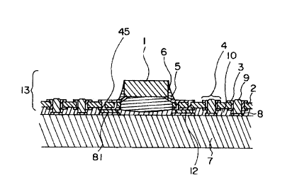
Referring to Fig. 1, an electronic device assembly according
to the first embodiment comprises a substrate 7 and a chip
carrier 13 mounted on the substrate 7.
In this exemplary embodiment, the substrate 7 is a glass-
epoxy substrate. However, other substrates such as ceramic
substrates can be used as the substrate 7. The substrate 7 has
pads 8 and 81 on the upper surface thereof. The pads 8 and 81
are preferably formed from copper and plated with gold.
The chip carrier 13 includes a flexible substrate 2, a
large-scale-integrated circuit (LSI) chip mounted on the flexible
substrate 2, and a resin 6 covering the lower surface of the LSI
chip.
In the exemplary embodiment, the LSI chip 1 is square-shaped
-6-
2151259
having a length of approximately 17.5 mm. The LSI chip 1 has
800 terminals along each of the sides thereof. The terminals
are aligned with approximately an 80 um pitch.
The flexible substrate 2 is made of an organic
insulating film. The flexible substrate 2 is preferably made
from materials having suitable heat resistance and a relatively
low thermal expansion coefficient. The flexible substrate 2 is
preferably easily attachable to conductor patterns. Materials
for the flexible substrate 2 include polyimide, fluorine-type
materials, and epoxy-type materials. In this exemplary embodi-
ment, the flexible substrate 2 has a thickness of about 50 um.
The flexible substrate 2 has a device hole in the
center portion thereof. Inner leads 5 are formed on the upper
surface of the flexible substrate and protrude above the device
hole. One end of the inner lead 5 is connected to a corres-
ponding terminal of the LSI. The inner lead 5 is encapsulated
in the resin 6.
Ref erring to Figs. 1 and 2(a), the flexible substrate
2 has a connecting structure 4. The connecting structure 4
includes a tapered through-hole 44, and conductive patterns 41,
42, and 43. The conductive patterns 41, 42, and 43 are formed
on the lower surface of the flexible substrate 2, the inner
surface of the through-hole 44, and the upper surface of the
flexible substrate 2, respectively. The conductive patterns
41, 42, and 43 are preferably formed from copper and plated
with gold.
The connecting structure 4 is connected to the corres-
ponding inner lead 5 via a wiring pattern 3 formed on the upper
surface of the flexible substrate 2. The wiring pattern is
preferably
66446-616
'' . 2157259
formed from copper and plated with gold. The thickness of the
wiring pattern is about 10 to 25 ~Cm.
Referring to Figs. 1 and 2(b), the flexible substrate 2 has
a connecting structure 45 along the side of the device hole. The
connecting structure 45 includes conductive patterns(ground
plane) 46 and 48 formed on the upper and lower surfaces of the
flexible substrate 2,, respectively. The conductive patterns 46
and 48 are connected by a via 47. The connecting structure 45
is connected to the corresponding inner lead 5 through the wiring
pattern 3. The connecting structure 45 has advantages in
reducing noise, avoiding cross-talk, and impedance matching.
Referring again to Fig. 1, a solder paste 12 connects the
connecting structure 45 and the pad 81. Solder 9 connects the
connecting structure 4 and the pad 8. A part of the solder 9 is
placed in the through-hole and appears on the upper surface of
the flexible substrate 2 to indicate a reliable connection.
A thermosetting resin 10 fills an area between the flexible
substrate 2 and the substrate 7 . The flexible substrate 2 is
attached to and integrated with the substrate 7 by the
thermosetting resin 10. The thermal expansion coefficient of the
resin 10 is preferably between those of the flexible substrate
2 and the substrate 7. The temperature at which the
thermosetting resin 10 begins to set is about 130 °C to 230 °C.
The melting temperature of the solder 9 and the solder paste 12
is about 180 °C to 230 °C. Epoxy-type resins and fluorine-type
resins can be.used as the thermosetting resin 10.
Next is described the manufacturing method of the first
embodiment.
_g_
66446-616
2157259
Referring to Fig. 3(a), in a first step, the solder 9
and the solder paste 12 are provided on the pads 8 and 81,
respectively. Before placing the solder 9 on the pad 8, a
solder paste may be applied on the pad 8 to attach the solder 9
to the pad 8.
Referring to Fig. 3(b), in a second step, the chip
carrier 13 is positioned so that the connecting structures 4 and
45 are placed on the solder 9 and the solder paste 12, respect-
ively. The LSI chip 1 is previously mounted on the flexible
substrate 2 by tape automated bonding.
Referring to Fig. 3(c), in a third step, the thermo-
setting resin 10 is applied over the upper surface of the
substrate 7 except for over the solder 9 and the solder paste
12. The thermosetting resin 10 may be injected through the gap
between the flexible substrate 2 and the substrate 7. The
thermosetting resin 10 may also be injected through an
injection hole provided in the flexible substrate2.
Referring to Fig. 3(d), in a fourth step, reflow
soldering is performed. The solder 9 melts to flow into the
tapered through-hole 44 and appears on the upper surface of the
flexible substrate 2. The connection failure of the solder 9
can easily be detected by confirming whether or not the solder
9 protrudes from the through-hole 44. As the solder 9 flows
into the through-hole 44, the flexible substrate 2 moves down to
contact the thermosetting resin 10 at the lower surface thereof.
The solder paste 12 also melts to connect the pad 81 and the
connecting structure 45.
In this reflow soldering, the thermosetting resin 10
is set. The flexible substrate 2 is attached to and integrated
with the
-9-
66446-616
2157259
substrate 7 by the setting of thermosetting resin 10.
Next is described the technical advantages of the first
embodiment.
In the first embodiment, the solder connection is protected
from mechanical stress and stress due to thermal cycling because
the flexible substrate 2 is attached to the substrate 7 by the
thermosetting resin 10. Moreover, the solder connection is
protected from relative humidity because the solder connection
is encapsulated in the thermosetting resin 10. Thus, the
reliability of the solder connection is enhanced.
The manufacturing process of the first embodiment is
relatively simple because the melting of the solder and the
setting of the thermosetting resin are performed by simultaneous
heating.
Next is described the second embodiment of the present
invention.
A key feature of the second embodiment is using a
thermosetting resin sheet instead of the thermosetting resin 10.
Other structures and functions are the same as those of the first
embodiment.
Referring to Fig. 4, in the second embodiment, a
thermosetting resin sheet 11 is provided between the flexible
substrate 2 and the substrate 7. The thermosetting resin sheet
11 has openings at positions corresponding to the pads 8 and 81.
The pads 8 and 81 are reachable through the openings.
The thickness of the thermosetting resin sheet 11 is
optimally selected so that a desired gap is formed between the
flexible substrate 2 and the substrate 7.
-10-
2157259
Next is described the manufacturing method of the
second embodiment.
Referring to Fig. 5(a), in a first step, the solder 9
and the solder paste 12 are provided on the pads 8 and 81,
respectively.
Referring to Fig. 5(b), in a second step, the thermo-
setting resin sheet 11 is placed on the upper surface of the
substrate 7. The solder 9 and the solder paste 12 are not
covered with the thermosetting resin sheet because of the
openings provided therein.
Referring to Fig. 5(c), in a third step, the chip
carrier 13 is positioned so that the connecting structures 4
and 45 are placed on the solder 9 and the solder paste 12,
respectively.
Referring to Fig. 5(d), in a fourth step, the solder
9, the solder paste 12, and the thermosetting resin sheet 11
are heated. The solder 9 melts to connect pad 8 and the
connecting structure 4. A part of the solder 9 flows into the
tapered through-hole 44. The solder paste 12 melts to connect
pad 81 and the connecting structure 45. The flexible
substrate 2 moves down to contact the thermosetting resin sheet
11.
In this heating, the thermosetting resin sheet 11 is
set simultaneously. The flexible substrate 2 is attached to
and integrated with the substrate 7 by the thermosetting resin
sheet 11.
Next is described the technical advantages of the
second embodiment.
-11-
..~~ 66446-616
2157259
In addition to the technical advantages of the first
embodiment, in the second embodiment, the gap between the
flexible substrate 2 and the substrate 7 can be selectively
controlled by changing the thickness of the thermosetting resin
sheet 11.
Next is described the third embodiment of the present
invention.
A key feature of the third embodiment is a connecting
member 93 interposed between the flexible substrate 2 and the
substrate 7. The other structures and functions are
substantially the same as those of the first embodiment.
Referring to Fig. 6, a connecting member 93 is inter-
posed between the flexible substrate 2 and the substrate 7.
The connecting member 93 includes a film 90 and conductive
bodies 91.
In this exemplary embodiment, the film 90 is formed
from epoxy-type materials or polyimide-type materials. A
ceramic sheet can be used instead of the film 90. In this
exemplary embodiment, the thickness of the film 90 is about 0.1
mm to 0.5 mm.
The conductive body 91 is preferably made from metals
such as gold and copper. The upper and lower portions of the
conductive body 91 protrude from the upper and lower surfaces
of the film 90, respectively. The upper and lower portions of
the conductive body 91 are coated with solder. The conductive
body 91 connects the pad 8 and the connecting structure 4. The
conductive body 91 connects the pad 81 and the connecting
structure 45. The upper portion of the conductive body 91 is
.,~ ~,
-12-
66446-616
2157259
inserted in the tapered through-hole 44 to position the
flexible substrate 2 precisely. The height of the conductive
body 91 is set so that a desirable gap (e. g., predetermined by
the designer) is formed between the flexible substrate 2 and
the substrate 7. In this exemplary embodiment, the height of
the conductive body 91 is about 0.2 mm to 0.5 mm.
A resin 101 fills an area between the substrate 7 and
the film 90. The thermal expansion coefficient of the resin
101 is preferably between those of the substrate 7 and the
film 90. A resin 102 fills an area between the film 90 and
the flexible substrate 2. The thermal expansion coefficient of
the resin 102 is preferably between those of the LSI chip 1 and
the film 90. In this exemplary embodiment, the resins 101 and
102 are thermosetting resins. However, other resins can
suitably be used as the resins 101 and 102 so long as they are
set by some means.
Next is described the manufacturing method of the
third embodiment.
Referring to Fig. 7(a), in a first step, the
substrate 7 is prepared.
Referring to Fig. 7(b), in a second step, the
connecting member 93 is positioned so that the lower portion
of the conductive body 91 is placed on the pad 8.
Referring to Fig. 7(c), in a third step, the chip
carrier 13 is positioned so that the connecting structure 4 is
placed on the upper portion of the conductive body 91. The
upper portion of the conductive body 91 is inserted into the
tapered through-hole 44. Thereafter, the conductive body 91
-13-
66446-616
2157259
is heated. The solder coated on the conductive body 91 melts
to connect the conductive body 91 to the pad 8 and the connect-
ing structure 4.
Referring to Fig. 7(d), in a fourth step, the resin
101 fills an area between the substrate 7 and the film 90.
The resin.
-13a-
66446-616
2157259
102 fills an area between the film 90 and the flexible substrate
2. Thereafter, the resins 101 and 102 are heated and set. The
flexible substrate 2, the connecting member 93, and the substrate
7 are integrated by the resins 101 and 102.
Next is described the technical advantages of the third
embodiment.
In the third embodiment, the reliability of connecting
portions is enhanced as in the first embodiment.
Further, the gap between the flexible substrate 2 and the
substrate 7 can be selectively controlled by varying the height
of the conductive body 91.
Next is described the fourth embodiment of the present
invention.
A key feature of the fourth embodiment is an anisotropic
conductive sheet 112 electrically connecting the flexible
substrate 20 and the substrate 7.
Referring to Fig. 8, the structures and functions of an LSI
chip 1, resin 6, and the substrate 7 are the same as those of the
first embodiment.
The chip carrier includes a flexible substrate 20, and LSI
chip mounted on the flexible substrate 20.
The flexible substrate 20 has a device hole in the center
thereof. Inner leads 5 are formed on the lower surface of the
flexible substrate 20. One end of the inner lead 5 protrudes
below the device hole and is connected to the terminals of the
LSI chip 1. Pads 21 are formed on the lower surface of the
flexible substrate 20. The pads 21 are preferably formed from
copper and plated with gold. The inner leads 5 and the pads 21
-14-
215725-9
are connected via wiring patterns (not shown) formed on the lower
surface of the flexible substrate 20.
An anisotropic conductive sheet 112 is interposed between
the flexible substrate 20 and the substrate 7. The pad 21 of the
flexible substrate 20 and the pad 8 of the substrate 7 are
electrically connected via the anisotropic conductive sheet 112.
The anisotropic conductive sheet 112 comprises a_thermosetting
resin and metallic particles dispersed in the thermosetting
resin. The thickness of the anisotropic conductive sheet 112 is
selectively set so that a desirable gap is formed between the
flexible substrate 20 and the substrate 7.
A resin 103 fills an area between the substrate 7 and the
anisotropic conductive sheet 112. The thermal expansion
coefficient of the resin 103 is preferably between those of the
substrate 7 and the anisotropic conductive sheet 112. A resin
104 fills an area between those of the anisotropic conductive
sheet 112 and the flexible substrate 20. In this exemplary
embodiment, the resins 103 and 104 are thermosetting resins.
Next is described the fourth embodiment of the present
invention.
Referring to Fig. 9(a), in a first step, the substrate 7 is
prepared.
Referring to Figs. 9 (b) and 10 (a) , in a second step, the
anisotropic conductive sheet 112 is placed on the pad 8. A
separator sheet 14 is attached to the upper surface of the
anisotropic conductive sheet 112 for easy handling. However,
separator sheet 14 is easily detachable from sheet 112.
Referring to Figs. 9(c) and 10(b), in a third step, the
-15-
2157259
separator sheet 14 is removed from the anisotropic conductive
sheet 112.
Referring to Figs. 9(d) and 10(c), in a fourth step,
the chip carrier 131 is placed on the anisotropic conductive
sheet 112 so that the pad 21 faces the corresponding pad 8 via
the anisotropic conductive sheet 112. Thereafter, the
anisotropic conductive sheet 112 is thermocompression bonded
to the pads 8 and 21. By this thermocompression bonding, the
thermosetting resin in the anisotropic conductive sheet 112 is
set. The metallic particles 15 in the thermosetting resin
concentrate (e.g., are positioned) between the pads 8 and 21.
Thus, the pads 21 and 8 are electrically connected.
Referring to Figs. 9(e) and 10(d), in a fifth step,
the resin 103 fills an area between the substrate 7 and the
anisotropic conductive sheet 112. The resin 104 fills an area
between the anisotropic conductive sheet 112 and the flexible
substrate 20. Thereafter, the resins 103 and 104 are heated
and set. Thus, the chip carrier 131, the anisotropic
conductive sheet 112, and the substrate 7 are integrated.
Next is described the technical advantage of the
fourth embodiment.
In the fourth embodiment, the reliability of the
connecting portion is enhanced as in the first embodiment.
Further, the gap between the flexible substrate 2
and the substrate 7 can be advantageously controlled by
varying the thickness of the anisotropic conductive sheet 112.
-16-
66446-616
,s
2151259
Moreover, the manufacturing process of the fourth
embodiment is relatively simple because a soldering step is
unnecessary.
-16a-
66446-616
2157259
The present embodiments are therefore, to be considered in
all respects as illustrative and not restrictive, the scope of
the invention being indicated by the appended claims rather than
by the foregoing description and all changes which come within
the meanings and range of equivalency of the claims are therefore
intended to the embraced therein.
-17-