Note: Descriptions are shown in the official language in which they were submitted.
WO 94/2100
PCT/DK94/00107
A connector element for telecommunication.
1
The present invention relates to a connector plug
or jack for use in communication networks, including
data transmission networks. The traditional copper wires
in these networks have been challenged by fibre optics,
which provides for a very high transmission capacity,
that is the ability of conducting a very high number of
bits per second. However, the copper wire system still
has pronounced advantages, and it has been possible to
develop the copper wire cables so as to achieve a no-
ticeable increase of the transmission capacity. A main
problem has been the electrical capacity between the
wises in a bundle of wires, but very good results have
been achieved by different measures such as a twisting
of the wires.
In connection with the invention, it has been re-
cognized that in these systems there is a bottle neck
problem associated with the use of the connector ele-
ments, in which it is common practice, derived from
already established standards, to arrange neat rows of
terminals which are connected with corresponding rows of
cable connector terminals through parallel conductors
inside the connector element. Inevitably, there will be
a certain capacitive coupling between these conductors,
and this coupling will be the stronger, the smaller the
distance is between the conductors. It is a pronounced
desire that the connector elements should be as small as
possible, and this, of course, will accentuate the pro-
blem, because the required small dimensions will imply a
small mutual distance between the internal leads of the
single connector elements and thus a relatively high
capacity between these leads.
However, while the capacity between neighbouring
conductors is relatively high, it may be undesirably low
between non-neighbouring conductors. The standard alrea-
dy set for the dedicated use of the single terminals are
not too lucky for the favouring of ideal conditions in
WO 94/21007
PCT/DK94/00107
2
the connector elements, and problems occur not only as
far as the capacities are concerned, but also with re-
spect to conductor inductance and mutual inductance, the
former being associated with the width of the conductors
and the latter with the coil effect of the pairs of
associated conductors.
The invention is believed to be a pioneer work in
the study of the interactions of these different pheno-
mena, but since the physical result of the invention
seems to be structurally new, it is deemed unnecessary
to describe the said phenomena in more detail. Of
course, the structure of the invention has to be closely
linked with the said, already established standards, but
such standards may change, and the connector according
to the invention may well be adapted to other standards.
In its basic concept, the invention breaks with the
traditional picture of the leads inside the connector
element extending practically parallelly with each other
between a row of connector terminals and a row of wire
receiving terminals, in that these leads, internally in
the connector unit, extend generally in a three-dimen-
sional space, such that different leads are spaced not
only laterally, but also perpendicularly to the plane of
the lateral spacing.
As far as the capacity is concerned, it is possible
to hereby maintain a desired distance between two leads
in the connector, while at the same time it is possible
to bring more closely together two non-neighbouring
leads for increasing the capacity between them.
With respect to the mutual inductance, it will
clearly make an important difference whether the coil
axis is.oriented one way or the other, and while the
axis is conventionally located perpendicularly to the
basic, common plane of the conductors, it will now be
possible to turn the direction of the axis into a more
or less inclined cross direction, by arranging for lends
WO 94/21007 .~.. ~ ~ PGT/DK94/00107
3
belonging to the same loops to be located one above the
other, whether or not additionally being staggered in
the transverse direction. The mutual inductance can be
largely affected and controlled in this manner.
Also the inductance of the single leads can be
adjusted, because once the leads are brought into a
three-dimensional pattern they can be arranged generally
with increased mutual distance, whereby their widths can
be varied somewhat without any major influence on the
capacities.
In practice, of course, the quantities of the capa-
city, the inductance and the mutual inductance-will be
highly interrelated in the structure, but in fact it has
been found possible to design the lay-out in such a
manner that the connector, seen electrically, simply
disappears, causing no disturbance in the signal trans-
mission even at~very high transmission capacities. The
detailed lay-out will depend on the standards used for
termination sequence and various electrical conditions,
but given the conditions, the structure according to the
invention will be widely adaptable thereto.
While the connector contact elements, normally made
as strip end portions of the said internal leads, are
desired - or prescribed - to be quite narrow and located
in a row with small mutual spacing, the wire connector
terminals cannot possibly be correspondingly arranged,
as they have to be much broader. In a known connector as
disclosed in US-A-5,186,647, this problem is overcome by
arranging the wiring terminals at both lateral sides of
the connector, but this adds to the overall width of the
connector. With the invention, thanks to the spatial
arrangement of the leads, it has been found possible to
arrange these tenainals in two rows, one behind the
other in a lower level, whereby the total width of the
connector can be kept small. Besides, it will be pos-
sible to mount all the wires by a single press-cap ope-
WO 94/21007 PCT/DK94/00107
4
ration, if the terminals are of the type provided with
upwardly open notches for receiving the wire ends and
cutting into the sides of these ends.
In the following, the invention will be described
in more detail, with reference tto the drawing, in
Which:
Fig. 1 is a perspective view of a connector unit
according to the invention, .
Fig. 2 is an enlarged perspective view of the in-
ternal leads of the connector, seen from the front end
thereof , _
Fig. 3 is a similar view, seen from the rear end,
Fig. 4 is a plan view of a section of a punched
strip member for forming the different leads in two
layers,
Fig. 5 is a top view of these layers when laid
together
Fig. 6 is a side view of the leads, according to
Figs. l and 2,
Fig. 7 and 8 are cross sectional views showing
different spatial dispositions of the leads
Fig. 9 is a perspective view corresponding to Fig.
1, but showing the unit in a more detailed manner, and
Fig. 10 is a perspective view of a finished connec-
tor, based on the unit shown in Fig. 9, and
Fig. 11 is a sectional view of the unit.
The connector unit shown in Fig. 1, has eight
contact springs 2 protruding at the front end of the
connector and being bent-over into their operative
positions, see also Fig. 6, in which they are shown in
dotted lines in that position. The leads of the
connector are cast into a plastic block 4, in which the
contact springs 2 are, respectively, connected with
individual wire connector terminals 6 arranged in two
rows with four in each row, viz. a foremost high level
row 8 and a rearmost low level row 10. Each of these
WO 94/Z1007 .
PCT/DK94I00107
inverted U-shaped terminals is provided with a notch 12
for receiving a horizontally disposed wire end, and on
the conductor block 4 they are marked with the uneven
figures 1-7 at the higher row 8, and (as indicated in
Fig. 3) with the even figures 2-8 at the lower row 10.
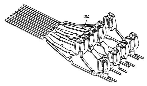
Figs. 2 and 3 show the packing of leads as made
ready for being cast into the body 4. The leads connect-
ing the wiring terminals in the rear row 10 with their
associated contact springs 2 extend in the plane of the
forwardly projecting, not yet bent-over contact springs
2, while only the inverted U-shaped terminals 6 are
provided as bent-up portions on these leads. At their
routs adjacent to the contact springs 2, the other four
leads are bent upwardly a short distance at 14, where-
after they extend rearwardly through a short horizontal
stretch 16 and then further through an upwardly inclined
stretch 18 to the inverted U-member forming the asso-
ciated terminal 6 in the upper terminal row, and there-
from further rearwardly through a downwardly inclined
stretch 20 and a following, rear stretch 23 almost in
level with the foremost horizontal stretch 16, i.e.
somewhat spaced above the level of the lowermost leads.
Also the lower terminals 6 have rearwardly projecting
portions.
The Figs. 2 and 3 will almost speak for themselves,
but they will be further commented upon later on in the
following.
The lead packing according to Figs. 2 and 3 is made
of two superimposed layers made, each, of four leads as
illustrated in Fig. 4. This figure shows a section of a
bronze strip 24, from which is punched, repeatedly, two
bottom layers 26 and two top layers 28, which layers are
then subjected to spatial shaping for the formation of
the terminals 6 and the raised runs 18, 20 of the upper
layer. Thereafter, the two different layers are con-
secutively superimposed and fed to an injection moulding
WO 94!21007 ~ ~ PCTIDK94100107
6
machine, in which they are provided with the block 4
according to Fig. 1. The immediate result is shown in a
more detailed view in Fig. 9, where the contact springs
2 are shown leaving the block 4 horizontally and with
their outer ends interconnected by an integral cross
strip 3 in each layer. After the moulding of the block 4
these strips are cut off and the springs are bent over
according to Fig. 1. -
Thereafter, as shown in Fig. 10, the unit is pro-
vided with a front frame member 5, which is secured by
snap locking into non-illustrated apertures in the
underside of the foremost flat portion of the block
unit.
In Fig. 10 is shown, in dotted lines, a press-cap
member 30 which, according to known principles, may
facilitate the mounting of the isolated connector wires
in the self-cutting type of wiring terminals 6, 12. For
such a mounting it could be natural to insert the strai-
ght wire ends into orderly arranged holes at the rear
side of the cap member, such that the wire ends would
automatically be pressed down into the correct terminals
when the cap is pressed down. However, the electrical
conditions are very critical, and instead of prescribing
such a mounting, see the wire pair A shown in
dot-and-dash lines in Fig. 6, it is found better to
arrange the wires as shown by the wire pair B in the
same figure, i.e. let in through the top of the presscap
30. The reason is that wires A, particularly the upper-
most wires, form loops together with the leads of the
connector, and it will be noted from Fig. 6 that the
areas of these loops will be considerably smaller for
wires B than for wires A. The wires B are mounted in the
press-cap as shown in Fig. 11.
In the example shown the connector is made accord-
ing to a specific standard, according to which the dif-
ferent terminals as numbered 1-8 in Fig. 1 should be
WO 94121007
~-~ ~ ~ ~ ~ PCTlDK94100107
used in pairs for different circuits, these pairs being
defined by the following terminals: 1-2; 4-5; 3-6; 7-8.
For at least one of these pairs it will be charac-
teristic that the associated leads 18 will be located
one above the other, such that the loop portion they
form will have its cross axis located horizontally or in
an oblique plane rather than vertically as in case of
leads running in parallel side by side. This is illu-
strated in Fig. 8, where the two leads a and b form a
coil portion having the field axis x. Another Wire pair
c, d is located in a vertical plane, thus having a hori-
zontal loop axis. These field orientations are signi-
ficant for the mutual inductance between the wire pairs.
It will be appreciated that from (or to) the tight-
ly disposed contact springs 2 leads inside the connector
are arranged in a very open structure. With the spatial
arrangement the distance between the leads, generally,
is largely increased, and it is possible to use leads of
varying width in order to optimize the inductances for
the desired result.
An important parameter to be balanced in the capa-
city between the leads, both of the single pairs and the
different pairs. Generally, the open structure con-
ditions reduced capacities, but still there is a need
for further reducing them at some places and for reduc-
ing them less at other places - or even increasing them.
Also this can be regulated thanks to the spatial struc-
ture, as now explained with reference to Fig. 7:
Fig. 7 shows three leads e, f and g arranged in a
spatial, triangular pattern. They should be compared
with a corresponding flat system, with lead g located in
the position marked g'. In that situation the capacity
between g' and e, as well as between a and f, may be
satisfactory, while it could be desired to increase the
capacity between g' and f. In a plane system this will
be practically impossible without adversely affecting
WO 94/21007 ~ ~ ~ ~ ~ PCT/DK94/00107
8
the other capacities, but if in a spatial system the
lead g' is swung along a circle centred in e, it will
maintain its capacity to a while increasing its capacity
to f. Thus, in position g it still has the desired capa-
city to a and a capacity to f increased as much as de-
sired.
Correspondingly, it is desired to decrease the
capacity between g' and f, without changing the capacity
g'-e, then a could be swung about g', away from f. Addi-
tionally, a may be arranged more or less close to g' for
changing even this capacity, and furthermore the widths
of the leads will influence the capacities.
Thus, also for this purpose it will be a character-
istic feature that once at least one of the leads has
attained a level above that of an underlying lead, as at
the bent-up lead portions 14, Fig. 2, there will be a
lateral displacement of the longitudinal extension of
one of these leads, not only for forming a non-horizon-
tal loop as already described, but also, that is either
additionally or alternatively, for adjusting relevant
capacities in the neighbourhood. Hereby the leads might
even cross each other in different planes, but so far no
such crossings have been found required, while - as
particularly clear form Fig. 5 - it is found advan-
tageous and possible to let the leads extend predomi-
nantly in pairs with the leads located one directly
above the other. As reflected by Fig. 5, however, there
is used five lead paths due to uneven horizontal spacing
between leads in the two layers. As to some other
details, Fig. 5 shows another design, in which for
example, the rear portions 23 are of different widths.
From Fig. 9 it is apparent that some lead portions,
designated 32, are exposed on the cast body 4. Such
exposed areas also occur at the underside of this body,
with a view to the optimizing of the dielectrical cover-
age of the leads at any place thereof.
WO 94/21007 ~ ~- ~ '~~ F~ r~ ~~ PCT/DK94/00107
9
Once the detailed structure of the lead system has
been determined and reduced to practice, i.e. stamped
out and spatially shaped, it will normally be a very
delicate matter to transfer the lead structure to the
die casting machine, since the accuracy requirements
will be extremely high. Thus, deviations or deformations
of just some hundredths of a millimetre may make the
connector unusable for the qualified purpose. On this
background the lead system is provided with various
portions such as protrusions 34, Fig. 3, and rear exten-
sions 20, 22 from the upper row of terminals 6 ~ such
that these portions can be gripped by suitable transfer
means. The presence of these electrically non-required
portions will call for special attention in the design
of the system, because they will inevitably affect at
least some of the operationally relevant parameters.
The connector shown is a female jack or socket
member for receiving a counterpart made as a plug with
rigid connector terminals. It will be understood that
such a plug may be designed widely similar to the dis-
closed jack or at least according to the same principles
with respect to the spatial arrangement of the leads.
Many modifications will be possible within the
scope of the invention, not only as far as the detailed
design of the illustrated leads is concerned. From a
practical point of view it is desirable that the leads
in the lower level extend in a common plane viz. the
bottom plane also comprising the originally punched-out
contact springs 2 according to Figs. 1 and 2, but it
will be an open possibility that these leads or some of
them might extend otherwise, upwardly or downwardly. The
same is true for the row of upper leads, which should
not necessarily be located in a common plane. Even the
terminals 6 will not have to be provided in line or
level with each other; for the electrical adaptation
there could be good reasons for arranging them other-
n ~~
_ eF s.:r
WO 94/21007 r ~ ~ ~ PCT/DK94/00107
l~
wise, but it will be appreciated that it is indeed prac-
tical to have them arranged in neat rows. Besides, it is
highly advantageous that these terminals, which are
potential high-capacity units, can be separated in the
longitudinal direction, while in the transverse direc-
tion they can be allowed to have a considerable, me-
chanically required width without making the entire
width of the connector element excessive. Besides, as
also apparent from the Figures, the terminals in the
single rows may be non-uniformly interspaced.
The two or even more rows of wire connection termi-
nals 6 may thus be located otherwise as shown,-and so
may the contact strips 2, which should not necessarily
be arranged in one neat row.