Note: Descriptions are shown in the official language in which they were submitted.
- 2157~23
CHARGE EQ~ALIZATION OF SERIES
CONNECTED CELLS OR BATTERIES
FIELD OF THE lNv~N,lON
This invention relates generally to the field of
battery charging and particularly to the charging of
multiple cells or batteries connected in series.
BACRGRO~ND OF THE lNV ~:N~ oN
Each type of electrochemical cell has a
characteristic "full charge" voltage. A lower cell voltage
indicates a-state of charge-less than "fulL". To obtain a
higher voltage than can be provided from a single cell,
cells are connected in series, often with internal or
integral connections between the cells, to form a battery
which has the desired level of output voltage. Certain
1~ types of electrochemical cells, such as rechargeable
alkaline manganese, lithium, and lithium ion ceils have no
internal charge control mechanism. Consequently, if
charging of such cells is not carefully controlled, over-
charge can result, which will cause irreversible changes in
cell che~istry, performance loss, and, in extreme cases,
21~7~23
._
-- 2
cell venting. The charging of series connected cells of
these types is therefore difficult, since cell voltages and
capacities may not be equal, with the result that some
cells are overcharged.
To address this problem, equalizers have been
developed which monitor the voltage across each cell and
connect resistors or current sinks across the cell or cells
having an excessive voltage to partially discharge the cell
and thereby accomplish charge equalization among the cells.
However, equalizing the charge on cells in this manner
wastes power and also causes undesirable heating of the
battery pack since the equalization circuitry is typically
physically located in the battery housing. In addition,
the rate at which the cells can be equalized, and thus the
rate at which the cells can be recharged, is limited to the
amount of power dissipation that can be tolerated.
SUMMARY OF T~E lNY~h~lON
Equalization of charge on multiple series
connected cells (or batteries) is accomplished in
accordance with the present invention rapidly and
substantially without unnecessary dissipation of power.
Equalization is accomplished automatically without
requiring comparison of voltages across individual cells or
batteries (cell units) and can be and preferably is carried
25 ~ out during charging of the cell units. Further, the
present invention provides current flow to a cell unit in
proportion to the difference in the voltages between cell
units, so that the lowest charged cell unit receives the
greatest charging current from the highest charged cell
unit while cell units at voltages intermediate the highest
and lowest (where more than two cell units are being
charged) receive lesser charge currents. Energy is
transferred in this manner from the most highly charged
cell unit to the cell unit or units having lesser charge.
~1~7823
.
-- 3
The equalizer apparatus of the present invention
includes a transformer having plural windings on a common
core, with one winding for each of the cell units to be
charged. All windings have the same number of turns and
are tightly coupled to one another (preferably using
multifilar wire) so that the leakage inductance of each
winding is minimal. A controllable switching device is
connected in series with each winding, and the series
combination of each winding and switching device is
connected in parallel across one of the cell units. An
oscillator is connected to the switching devices to provide
a control signal to each switching device to turn them on
and off simultaneously at a high switching frequency. The
switching frequency is preferably above the audible range,
e.g., preferably 20kHz or higher. A separate battery
charger may simultaneously supply charging current to the
series connected cell units.
~en the switching devices are turned on, the
voltages across all of the windings will be essentially the
voltage across the most highly charged cell unit, from
which current will flow into the transformer winding
connected to that cell unit. Current will flow out of the
windings connected to the lesser charged cell units, thus
transferring energy from the most highly charged cell unit
to the lesser charged cell units. Where more than two cell
units are being charged, the current from the most highly
charged cell is divided in the windings connected to the
other cell units in proportion to the difference in voltage
between the most highly charged cell unit and each of the
other cell units.
Because control of power flow is carried out by
switching elements which are either on or off, very little
power loss occurs in the equalization circuit and very
little heating of the components occurs. Consequently,
equalization can be carried out at a very rapid rate
compared to conventional equalization circuits, and the
equalization is carried out with high energy efficiency.
2157823
-
-- 4
The high switching frequency is high enough and preferably
beyond the audible range so that operation is substantially
noiseless. Because the transfer of energy from the most
highly charged cell unit to lesser charged cell units is
carried out automatically by the inherent operation of the
circuit, no complex voltage comparator circuits are
required, minimizing the complexity and expense of the
circuit. In addition, because no voltage measurements need
be made, the present invention operates without regard to
temperature and no compensation is required for temperature
changes which may result in changes in cell unit voltages.
The equalizer of the invention may also include a
second winding and a second switching device connected
together in parallel with the first winding and first
switching device for each of the cell units. An oscillator
is connected to the first and second switching devices for
each cell to turn them on and off alternately, so that when
each of the first switching devices is turned on, the
second switching devices are turned off, and conversely,
when the second switching devices are turned on, the first
switching devices are turned off. In this manner, charging
current can be delivered from the most highly charged cell
unit to the lesser charged cell unit during both halves of
the switching cycle, allowing even more rapid equalization
of the cell units, while making more efficient use of the
B-H curve of the transformer core and allowing the
transformer size to be-reduced.
Further objects, features and advantages of the
invention will be apparent from the following detailed
description when taken in conjunction with the accompanying
drawings.
BRIEF DESCRIPTION OF THE DRAWINGS
In the drawings:
Fig. 1 is an illustrative block diagram of the
equalizer of the present invention connected to provide
2157823
-
-
-- 5
equalization of two series-connected cell units being
charged.
Fig. 2 is a schematic circuit diagram of an
equalizer in accordance with the present invention for
providing equalization of the charge to two cell units.
Fig. 3 is a simplified equivalent circuit for a
portion of the equalizer of Fig. 2.
Fig. 4 is a schematic circuit diagram of an
equalizer apparatus in accordance with the invention for
providing equalization of the charge on more than two cell
units.
Fig. 5 is a schematic circuit diagram of an
equalizer of the invention which is connected to two cell
units to provide equalization current between the cell
units during both halves of the switching cycle.
DETAILED DESCRIPTION OF THE lNv~N~lON
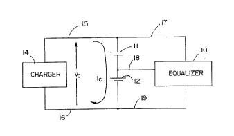
With reference to the drawings, a block diagram
of a charging system is shown in Fig. 1 which includes the
equalizer 10 of the present invention connected to two
series connected electrochemical cell units 11 and 12. The
cell units 11 and 12 may comprise various types of
electrochemical cells, such as lithium-ion, rechargeable
lithium, and rechargeable alkaline manganese batteries of
the type commonly used in, e.g., cellular phones, videotape
recorders and players, cameras, cordless tools, portable
communications equipment, electric vehicles, and so forth.
Although the problem is most acute for equalization of
charge for individual cells of this type connected in
series, the cell units 11 and 12 may comprise batteries of
internally or externally connected cells where a
requirement exists to properly equalize the charge across
the two or more separable cell units. As used herein, the
term "cell unit" is intended to refer both to single cells
and to internally or externally connected batteries of
cells. The illustrative charging system of Fig. 1 includes
7~23
-
-- 6
a charger 14 which supplies a charging current Ic on
connecting lines 15 and 16, with the charging current Ic
passing in series through the batteries 11 and 12. The
charger 14 may be any type of conventional charger
including constant current, float and trickle chargers,
which are well known in the art. The output voltage of the
charger 14, Vc, is applied across the series connected cell
units 11 and 12. A connecting line 17 extends from the
equalizer 10 to the positive terminal of the cell unit 11
and a connecting line 18 extends from the equalizer to the
negative terminal of the cell unit 11 and to the positive
terminal of the cell unit 12. Another connecting line 19
extends from the equalizer to connection to the negative
terminal of the cell unit 12. Although the equalizer 10 is
thus effectively connected in parallel with the cell units
11 and 12 across the charger 14, it draws substantially no
power from the charger. The equalizer 10 of the invention
may be utilized with various types of standard chargers
which utilize various charging schemes, such as trickle
chargers and constant current chargers, since the equalizer
10 does not draw significant power from the charger 14. It
is also understood that the equalizer 10 may operate, if
desired, when the charger 14 is not charging the cell
units. As described further below, the equalizer 10 may be
automatically actuated when the charger 14 supplies current
to the cell units 11 and 12.
A schematic circuit diagram of an embodiment of
the equalizer 10 for supplying the two cell units 11 and 12
is shown in Fig. 2. The equalizer 10 includes a
transformer 21 having a core 22 about which is wound a
winding 23 and a winding 24. The windings 23 and 24 are
preferably formed of bifilar wires (e.g., No. 28 AWG wire)
which are wound together on the core 22 with a very small
gap (e.g., less than 0.001 inch). Because the windings 23
and 24 are formed of bifilar windings, each has an equal
number of turns (e.g., 30 turns). The core 22 may be an E-
core (e.g., 41205-EC, "J" material, available from Magnetic
` ` 21~7823
_
Devices, Inc. of Crystal Lake, Illinois; or 1408-3C8 POT
Core). The winding 23 is connected to the line 17 leading
to the positive terminal of the cell unit 11. One end of
the winding 24 is connected by the line 18 to the negative
terminal of the cell unit 11 and to the positive terminal
of the cell unit 12. A controllable switching device 26
such as a power MOSFET (e.g., MTP25NO6L) is connected to
the winding 23 and by a conducting line 27 to a node 28 to
which the line 18 is connected. The series combination of
the winding 23 and the switching device 26 is thus
connected in parallel across the cell unit 11. Another
switching device 30 is connected to the winding 24 and, by
a line 31, to the line 19 leading to the negative terminal
of the cell unit 12. Thus, the series combination of the
winding 24 and the switching device 30 is connected in
parallel across the cell unit 12. The controlled switching
device 30 may also be a power MOSFET (e.g., MTP25NO6L).
An oscillator chip 34 (e.g., HA7555; TLC555) has
a resistor 35 and a capacitor 36 connected thereto to
provide a square-wave output signal on a line 38 at a
desired frequency (for the values of resistances and
capacitance shown in Fig. 2, at 25kHz). A conducting line
39 is connected from the ground pin of the chip 34 to the
line 31 and thus to the negative terminal of the cell unit
12, and line 40 is connected from the supply voltage pins
of the chip 34 to a line 41 which is connected to the line
27, and thus to the positive terminal of the cell unit 12
to provide power to the chip 34. The square-wave output
voltage signal on the line 38 from the chip 34 is provided
(through a resistor 43) to the gate 44 of the MOSFET 30 and
is coupled through a capacitor 45 to the gate 46 of the
MOSFET 26. The capacitor 45 provides DC voltage isolation
of the gates 44 and 46 while essentially passing the
square-wave voltage signal from the chip 34 to the gate 46
so that substantially the same waveform is present at the
gate 46 as at the gate 44. Consequently, the MOSFET's 26
and 30 are turned on and off simultaneously at the
21~i7823
-- 8
switching frequency of the oscillator 34. To maintain the
gate 46 properly referenced to the source of the MOSFET 26,
a paralleled diode 48 and resistor 49 are connected between
the source and the gate 46. As shown in Fig. 2, a
capacitor 50 may be connected between the line 17 leading
to the positive terminal of the cell unit 11 and by the
lines 41, 27 and 18 to the negative terminal of the cell
unit 11, and a capacitor 51 may be similarly connected
between the line 18 leading to the positive terminal of the
cell unit 12 and a line 19 leading to the negative terminal
of the cell unit 12, for snubbing purposes when the cells
are at a substantial physical distance from the equalizer
10 and wiring inductance is a factor.
The oscillator 34 provides substantially a
square-wave output signal to the gates 44 and 46 of the
MOSFET switches 30 and 26, respectively. These switches
are thus turned on and off simultaneously for approximately
equal periods of time. When the switches are turned on,
the voltage from the-cell unit 11 will be imposed across
the winding 23 and the voltage from the cell unit 12 will
be imposed across the winding 24. Because the windings 23
and 24 have exactly the same number of turns and are
tightly coupled, the voltage of the more highly charged
cell unit, either the unit 11 or 12, will appear across
both of the windings 23 and 24. For example, if the cell
unit 11 is more highly charged than the cell unit 12, the
voltage across the windings 23 and 24 will be the voltage
of the cell unit 11, and current will flow through the cell
unit 11 in a direction from the negative toward the
positive terminal and through the winding 23, inducing a
current in the winding 24 which will flow in a direction
from the positive terminal to the negative terminal of the
cell unit 12. Consequently, during the time that the
switching devices 26 and 30 are on, energy will be
transferred from the cell unit 11 to the cell unit 12. The
level of current flow will be directly proportional to the
difference between the voltages on the cell units 11 and
21~7~3
12. As the voltages of the two cell units approach one
another, the level of current flow decreases and becomes
substantially zero when the two cell units are equally
charged. It is seen that any charging current Ic flowing
from the charger 14 will have no effect on this
equalization since the charging current should
substantially all flow through the relatively low
resistance of the cell units 11 and 12 rather than through
the windings 23 or 24.
As any real transformer, the transformer 21 has
some primary inductance in which energy is stored when the
switches 26 and 30 are on. When the switches turn off,
this energy must be released. Rather than being
dissipated, this energy may be recovered and transferred
back to the cell unit, as illustrated in Fig. 3 which shows
simplified equivalent circuits for the MOSFET switches 26
and 30. The switch 26 has an effective drain to source
capacitance 26a and a body diode 26b, and the switch 30 has
a drain to source capacitance 30a and a body diode 30b.
When the switches 26 and 30 are turned on, a current I
flows from the cell 11 or 12 which has the highest voltage
and the energy stored in the transformer inductance L is
1/2 LI2. When the switches 26 and 30 are turned off, this
energy is transferred to the capacitor 26a or 30a, with the
energy stored in the capacitor being equal to 1/2 CV2, where
C is the capacitance of the capacitor and V is the voltage
across the charged capacitor. By proper selection of the
core, turns and gap of the transformer 21 to obtain a
selected primary inductance L, and selection of the
capacitance C of the switching devices 26 and 30, the
resonant circuit formed by the transformer and the
switching devices allows resonant energy recovery as long
as the frequency of the switching, as controlled by the
oscillator 34, is less than 1/2~ ~ .
The present invention may be extended to the
equalization of more than two cell units, as illustrated in
the schematic circuit diagram of Fig. 4. Here, in addition
21~7~3
-
-- 10 --
to the cell units 11 and 12, two additional cell units 60
and 61 are connected in series. A transformer 65 has a
core 66 to which four windings 67, 68, 69 and 70 are wound.
For example, the windings 67-70 may be quad-filar wound
S (e.g., No. 28 AWG wire, 28 turns) on a small gap core
(e.g., 1408-3C8POT with a 0.0001 to 0.001 inch gap to
prevent remanence caused core saturation). Four switching
devices (e.g., MTPSOH06EL MOSFETs) 72-75 are connected to
the windings such that one of the switching devices is
connected in series with one of the windings. Each series
combination of winding and switching device is connected in
parallel across one of the cell units, i.e., the winding 67
and switch 72 across the cell unit 11, the winding 68 and
switch 73 across the cell unit 12, the winding 69 and
switch 74 across the cell unit 60, and the winding 70 and
switch 75 across the cell unit 61. An oscillator 80 (e.g.,
a CMOS 555 timer) has a capacitor 81 and resistor 82
connected to the pins thereof to select the frequency of
oscillation of the oscillator 80, e.g., at 25kHz. The
square-wave output signal from the oscillator 80 is
provided on a line 84 through a resistor 85 directly to the
gate of the switching device 75 and through capacitors 87,
88 and 89 to the gates of the MOSFETs 74, 73 and 72.
Alternative parallel connections for the capacitors 88 and
89 are shown in dashed lines in Fig. 4. Resistors and
diodes are connected to the gates of the MOSFETs 72-74 for
the reasons described above. When the switching devices
72-75 are turned on, the voltage appearing across each of
the windings 67-70 will be the voltage across the most-
highly charged cell unit 11, 12, 60 or 61. Thus, charging
of the undercharged cell units will take place in
proportion to the voltage difference between that cell unit
and the most-highly charged cell unit.
It is preferable that the equalizer of the
invention not be operating when charging is not taking
place to maximize the shelf life of the battery. To turn
off the equalizer, a signal may be provided on a line 90
21S7823
-- 11 --
extending to the base of a bipolar transistor 91.
Resistors 92 and 93 are connected in series between the
positive terminal of the cell unit 11 and the collector of
the transistor 91, and the emitter of the transistor 91 is
connected to a line 94 which is connected to the negative
terminal of the cell unit 61. The junction between the
resistors 92 and 93 is connected to the base of another
bipolar transistor 96. When the voltage applied to the
line 90 is at zero volts, the transistor 91 is off, as is
the transistor 96. The transistor 96 is connected by a
line 98 to the voltage supply inputs of the oscillator chip
80. Thus, in this state, no power is supplied to the
oscillator 80, and it is turned off, applying no control
signal to the gates of the MOSFETs 72-75. Since these are
then off, no equalization current flows between the cell
units 11, 12, 60 and 61. When the charger 14 is on, a high
voltage is applied to the line 90, turning the transistors
91 and 96 on. Power is now supplied to the oscillator chip
80 so that it puts out a square-wave output signal to the
gates of the switches 72-75. While the transistor 91 is
on, a relatively small amount of power is dissipated in the
resistors 92 and 93.
Another embodiment of the equalizer of the
invention is shown in Fig. 5 which allows equalization
current to flow during both halves of the switching cycle.
The equalizer of Fig. 5 essentially uses two equalizer
circuits as in Figs. 2 or 4, each one operating on a
different half of the switching cycle. The equalizer of
Fig. 5 has a transformer 100 with a core 101 on which are
wound first windings 102 and 103 which are bifilar
windings. In addition, the transformer 100 also has second
windings 105 and 106 which are bifilar windings.
Preferably, the windings 102/103 and 105/106 all have the
same number of turns te.g., 20). A MOSFET switch 108
(e.g., MTP3055EL) is connected in series with the winding
102 across the cell unit 11. The winding 103 and a MOSFET
switch 109 are connected across the cell unit 12. A MOSFET
~1~7~23
- - 12 -
switch 111 is connected in series with the winding 105
across the cell unit 11, and a MOSFET switch 112 is
connected in series with the winding 106 across the cell
unit 12. The switches 108 and 109 may be considered
together as the "first" switches and the switches 111 and
112 as the "second" switches. Additional cell units may be
equalized by utilizing additional windings and switches in
the manner shown in Fig. 4.
An IC chip llS comprising a hex inverting Schmitt
trigger circuit (e.g., CMOS 74C14) is ~iased with a
resistor 116 and a capacitor 117 to act as an oscillator,
putting o~t a square-wave signal at a selected frequency,
e.g., 30kHz. One of the ou~u-s of the oscillator circuit
115 is a "non-inverted" ~u~, and is connected
through a line ll9 to the gates of the MO$FETSs
lQ8 and lO9, and another output of the circuit 115,
connected to a line 120, is -the "inverted" output
and is provided to the gates of the ~IOSFETs lll and
112. The signals on the lines 119 and 120 are the
complements of one another. When the signal on the line
119 is "high", the signal on the line 120 is "low" and vice
versa; thus, when the MOSF~Ts 108 and 109 are on, the
MOSFETs 111 and 112 are off, and vice versa. When the
MOSFETs 108 and 109 are on, the voltage across each of the
windings 102 and 103 is the voltage of the more highly
charged of the cell units 11 and 12, whereas when the
MOSFETs 111 and 112 are on, the voltage across each of Ihe
windings 105 and 106 is the voltage across the more highly
charged of the cell units 11 or 12. Thus, energy is
transferred from the more highly charged to the less highly
charged cell unit on both halves of the switching cycle,
allowing more rapid equalization of the two cell units 11
and 12 than with the equalizer of Fig. 2. This arrangement
also makes more efficient use of the B-~ curve of the
transformer core, which allows the size of the transformer
to be reduced.
The oscillator llS is provided with supply
voltage from a line 122 which is connected to the positive
` ` 21~37~23
-
- 13 -
terminal of the cell unit 11, while the negative terminal
of the cell unit 12 is connected by a line 123 to the
neutral or ground pin of the circuit 115. To allow control
of the operation of the equalizer, a normally open relay
switch 126 may be connected?in the line 122 which is
operated by a relay coil 12/7 connected in the line 15 from
the charger 14. When current flows in the line 15 from the
charger 14 to thereby energize the coil 129, the switch 126
is closed, supplying power to the oscillator IC 115, and
thereby beginning switching of the MOSFETs 108, 109, 111
and 112. When the charger is off, and no current is
flowing through the coil 129, the switch 126 is opened, so
that all of the MOSFET switches are turned off and no power
is drawn by the equalizer circuit.
It is understood that the invention is not
confined to the particular embodiments set forth herein as
illustrative, but embraces all forms thereof as come within
the scope of the following claims.