Note: Descriptions are shown in the official language in which they were submitted.
2157986
Title: SYNC SEPARATOR AND VIDEO SIGNAL DETECTOR CIRCUITS
FIELD OF THE INVENTION
This invention relates to sync separator circuits and to video
signal detection. More particularly, it relates to circuits which provide
5 more accurate sync tip clamping, more accurate sync slicing, and more
reliable video signal detection.
BACKGROUND OF THE INVENTION
Composite video signals include a synchronization
component or a sync signal. The sync signal must be separated or sliced
10 from the composite video signal, usually at a fifty percent level which is
preferably halfway between the blanking level and the sync tip level. This
is usually implemented by systems which clamp the sync tip to a known
voltage and then sample the blanking level. Unfortunately, the clamps
commonly used for this purpose have a number of disadvantages, e.g. the
15 clamped output voltage tends to droop, and the droop varies with the
input duty cycle. In addition the clamps commonly used cause sync tip
distortion, and the clamped output tends to ride on the sync tip noise.
In addition, precision sync separator circuits are required to
accurately slice or separate the input video signal sync pulse at the fifty
20 percent level for signal amplitudes ranging from 0.5 volts peak to peak to
2.0 volts peak to peak or higher (e.g. 4 volts p-p). When the signal
amplitude changes rapidly, e.g. from 2.0Vp-p to 0.5Vp-p, the sync separator
slicing level can be higher than the sync amplitude in a typical slow
recovering sync separator circuit. This can result in incorrect slicing of the
25 video signal and loss of the sync signal.
In addition, difflculty can be encountered in reliably detecting
the presence of a video signal. In the design of a video detector circuit,
appropriate criteria must be chosen to determine whether a valid video
signal has been received. If the evaluation criteria are too strict, a valid
30 video signal corrupted with impulse noise and random time base errors
2157986
will not be detected. However if the evaluation criteria are too loose, large
amplitudes of pure noise may be detected as a valid signal.
BRIEF SUMMARY OF THE INVENTION
Therefore the invention in one of its aspects provides
improved sync tip clamping. In this aspect the invention provides an
improved clamping circuit for clamping sync signals in a video signal, said
.
clampmg clrcult comprlsmg:
(a) an input for said video signal, said video signal having
sync pulses therein,
(b) a capacitance coupled to said input,
(c) symmetrical clamping means and non-symmetrical
clamping means each coupled to said capacitance,
(d) said symmetrical clamping means comprising amplifier
means having an output coupled to said capacitance,
said amplifier having an enable input and an input for a
first reference voltage, said amplifier being controllable
by an enable signal applied to said enable input for
clamping the voltage at said output to said first refer~l~ce
voltage,
(e) means for providing an enable signal responsive to said
sync pulses for enabling said amplifier to cause said
amplifier to clamp the voltage at its output to said
rererel.ce voltage during at least a portion of each sync
pulse,
(f) said non-symmetrical clamping means including means
for charging said capacitance to a predetermined
minimum voltage level,
(g) said non-symmetrical clamping means further
including means responsive to the absence of a
continued series of said sync pulses for discharging said
capacitance.
2157986
--3 -
In a second aspect the invention provides a sync slicing
detector circuit which can recover more quickly than has previously been
the case from rapid changes in input video signal level. In this aspect the
invention provides, in a sync separator circuit having an input for
5 receiving an input video signal containing sync pulses, and circuit means
for adaptively slicing said sync pulses at a predetermined percentage of the
level of the sync pulses, an improved circuit means for reacting to changes
in the level of sald sync pulses, said improved circuit means colnprising:
(a) means for processing said video signal to produce a
clamped video signal,
(b) slicing circuit means for slicing said sync pulses at said
percentage to produce a sliced signal,
(c) first comparator means for comparing said clamped
video signal and said sliced signal and for producing a
composite sync signal therefroll-,
(d) means for providing a refer~llce signal,
(e) second comparator means for comparing said clamped
video signal and said reference signal for producing a
rererence sync signal,
(f) processing means for processing said composite sync
signal and said rerele,lce sync signal and for producing a
fault signal if the level of said composite sgnc signal has
a predetermined relationship with said refer~llce sync
signal,
(g) and means responsive to the presence of said fault signal
for lowering the voltage level at which said slicing
circuit means slices said sync pulses.
In a third aspect the invention provides a video signal
detector circuit which provides video signal detection of improved
reliability even in the presence of noise. In this aspect the invention
provides a video signal detector having a video signal input for receiving
a video signal having a series of sync pulses, and having at least one sync
2157g86
signal output, and for enabling said output when a valid video signal is
present at said input and for muting said output when no valid video
signal is present at said input, said circuit comprising:
(a) circuit means coupled to said input for producing a
reference sync signal having reference sync pulses at a
frequency colle~ponding to that of said sync signal,
(b) counter means for counting a predetermined number of
said reference sync pulses and for producing a
predetermined count signal on receipt of said
predetermined number,
(c) output circuit means coupled to said counter means and
responsive to said predetermined count signal for
enabling or muting said output in response thereto,
(d) frequency circuit means responsive to the frequency of
said sync pulses and for producing a memory signal
indicative of whether said frequency is within a
predetermined range,
(e) disabling means coupled to said frequency circu* means
for causing said output to be muted when said frequency
is outside said predet~rmined range.
Further objects and aspects of the invention will appear from
the following description, taken together with the accompanying
drawmgs.
BRIEF DESCRIPTION OF THE DRAWINGS
In the accompanying drawings, which show preferred
embodiments of the invention:
Fig. 1 is a view of a standard NISC composite video signal;
Fig. 2 is a block diagram of a standard prior art sync tip clamp;
Fig. 3 is a block diagram of an improved sync tip clamp
according to the invention;
Fig. 4 shows sync tip clamping sign~ls produced by the circuit
215 79~
of Fig. 3;
Fig. 5 shows pre-equalizing period clamp signals produced by
the circuit of Fig. 3;
Fig. 6 is a block diagram of a sync slicing detector according to
5 the invention;
Fig. 7 is a view showing video and sync signals processed by
the circuit of Fig. 6;
Fig. 8 is a view similar to that of Fig. 7 but showing fault
processing and detection signals from the circuit of Fig. 6;
Fig. 8A is a block diagram of an implementation of the 50%
level portion of the Fig. 6 detector;
Fig. 8B is a detailed circuit implementation of the Fig. 8A
block diagram;
Fig. 9 is a block diagram of a video signal detector according to
15 the invention;
Fig. 10 is a view of signals from the circuit of Fig. 9;
Fig. 11 is a diagram of further signals produced by the circuit
of Fig. 9;
Fig. 12 is a further diagram of signals produced by the Fig. 9
20 circuit; and
Fig. 13 is a block diagram showing how the circuits previously
described may be combined.
DETAILED DESCRIPTION OF PREFERRED EMBODIMENTS
Reference is first made to Fig. 1, which shows a standard
25 NTSC composite video signal 10. This signal is shown for illustration
purposes only since it will be re~li7e(1 that the invention may be used with
other video standards, e.g. PAL, SECAM, and others.
As shown, the composite video signal 10 includes a video
signal portion 12, a front porch section 14 (typically 1.5 microseconds iO.1
30 microsecond), a sync pulse 16 (typically 4.7 microseconds +0.1
microsecond), a bree;c~vay section 18 (typically 0.6 microseconds), a color
.. ~ , 2l5798~
-6-
burst 20 (typically 2.5 microseconds), and a color back porch 22 (typically 1.6
microseconds). The amplitude of a typical standard signal is 140 IRE above
the sync tip 24 (where 140 IRE equals 1.0 volts). The blanking level 26 is
typically 40 IRE above the sync tip 24 (as is the back porch level), and the
ideal 50% slicing level 30 is 20 IRE above the sync tip level 24 and 20 IRE
below the blanking level 26.
Derivation of the 50% slicing level 30 can be achieved either
by measuring the sync amplitude directly or by using an automatic gain
control (AGC) circuit to amplify or attenuate the sync amplitude to a
known level. In both cases, such systems require a clamping type circuit
and a sampling and holding type circuit. Either the sync tip 24 is clamped
and the blanking level 26 is sampled, or else the blanking level 26 is
clamped and the sync tip 24 is sampled. Most systems clamp the sync tip 24
and sample the blanking level 26 since this approach has simpler start-up
constraints.
Circuits which clamp the sync tip 24 and sample the blanking
level 26 normally clamp the sync tip to a known voltage. Since the sync
tip is the most negative part of the video signal, a negative peak clamp is
used. Fig. 2 shows a common prior art clamp for this purpose. In the Fig.
2 circuit, which is essentially a DC reslorer, a video signal source 32 having
a source impedance Rsource provides the clamp input signal 34 (which is
simply the composite video signal 10 of Fig. 1). The clamp input signal 34
is AC coupled through capacitor C1 to the inverting input 36 of
operational amplifier 38. Operational amplifier 38 has unidirectional
negative feedback via diode D1 connected between its output 40 and its
inverting input 36. A reference voltage Vref is connected to the non-
inve~ g input 42 of operational amplifier 38, while a current source IdiS (a
discharge current source) is connected between ground and a node 44
between capacitor C1 and h~vellh~g input 36.
The clamp output signal 46 (which is simply the clamp
input signal, now clamped) appears at node 44.
In operation, when the clamp output signal 46 is lower than
2157986
Vref, operational amplifier 38 charges capacitor Cl via negative feedback
diode Dl. When the clamp output is higher than voltage Vref, diode Dl is
non-conductive and current source Idis slowly discharges capacitor Cl.
Once steady-state operation is reached, the most negative part
5 of the input signal will be clamped to Vref. However since IdiS is
continually discharging capacitor Cl, there is a line to line droop in the
clamped output given by:
Vdroop Cl ( f Tsync~ (1)
where fscan = Horizontal scan rate
and Tsync = Sync pulse width
The Fig. 2 circuit has four problems that render it inadequate for sync tip
clamping in precision 50% sync separation systems.
The first problem is that the voltage Vdroop varies depending
on the value and manufacturing tolerances of Idis. This creates a problem
15 because the slicing point changes by an amount equal to the amount of
change in VdrOop~ Equation 1 shows that the amount of droop is directly
proportional to Idis. Therefore, as Idis varies over process tolerances and
temperature, the slicing level will also vary. A typical solution to this
problem is to make capacitor Cl large and Idis very small (so that Vdroop is
20 small). However this is an undesirable solution since it decreases the low
frequency or hum rejection of the circuit.
The second problem, which is closely related to the first
problem, is that VdrOop varies with the input duty cycle. As will be seen
from equation 1, as Tsync becomes larger, Vdroop will become smaller. The
25 resulting change in Vdroop~ as before, changes the point at which the input
signal is sliced. This problem becomes noticeable during the vertical sync
time, when Tsync changes from 4.7 microseconds to 54 microseconds.
The third problem is that the clamp of Fig. 2 causes sync tip
distortion. Any charge that is removed from the input coupling capacitor
30 (by Idis) during non-sync periods must be restored during sync. The
current needed to restore the charge flows through the input source
2157986
resistance Rsource and causes a voltage drop across this resistance. This
voltage drop appears as sync tip distortion. To a good approximation the
amount of distortion can be calculated by the following:
Vdistortion ~ourcelcharge~
f sync
= RsourceIdiS T (2)
sync
It is apparent that Vdistortion increases directly with the
magnitude of Idis
The fourth problem results from the fact that the clamp of
10 Fig. 2 is non-symmetrical. A non-symmetrical clamp is one in which the
charging and discharging currents are unequal. In the Fig. 2 circuit the
charging current is the maximum positive output current from
operational amplifier 38, which is typically one hundred times larger than
the discharge current Idis. This results in the clamp reacting quickly to
15 negative going pulses but very slowly to positive going pulses. Hence the
clamped output level effectively rides on the negative sync tip noise,
which is undesirable when the video signal is corrupted by noise.
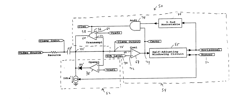
An improved clamping circuit according to the invention is
shown at 50 in Fig. 3. In. circuit 50, parts corresponding to those of Fig. 2
20 are shown with primed referellce numerals.
The clamping circuit 50 includes a non-symmetrical clamp 52
and a symmetrical clamp 54. The symmetrical clamp 54 includes a circuit
55 which is referred to as a "self-adjusting windowing circuit". Circuit 55 is
~les~rihed in detail in U.S. patent 5,432,559 issued July 11, 1995 and entitled
25 "Self-Adjusting Windowing Circuit with Timing Control", assigned to
the assignee of the present invention. The drawings and description of
that patent are hereby incorporated in their enliLely into this application by
this reference.
In the Fig. 3 circuit, a controlled transconductance amplifier
30 56 has a control input 58, and has its output 60 connected to node 44'
which is also connected to its inverting input 62. When enabled at control
21~7986
input 58 by enable signal Clen, amplifier 56 functions to charge or
discharge capacitor C1' to equate the clamp output 46' with a reference
voltage Vref2 applied to the non-inverting input 64 of amplifier 56. It is
only during the composite sync pulses 16 that amplifier 56 is enabled and
then by its action clamps the sync tips 24 to Vref2.
The clamp output 46', i.e. the clamped video signal (as shown
in Fig. 4), is applied to the inverting input 66 of a comparator 68. A 50%
level signal 70, which is representative of the 50% slicing level 30, is
applied to the non-inverting input 72 of comparator 68. (The manner in
which signal 70 is obtained will be explained below.) The difference
between the two signals, i.e. the raw composite sync signal Csync, is output
at the output 74 of comparator 68. Signal Csync is shown in Fig. 4 and may
include noise pulses 75, when impulse noise 75a crosses the 50% level 30.
In order to provide reliable clamping in the presence of noise,
it is desirable that the enable signal Clen applied to control input 58 of
amplifier 56 be noise tolerant. To achieve this objective, the enable signal
Clen is generated using the self-adjusting window circuit 55 in
conjunction with a monostable 76 (shown as having a 3.5 microsecond
period), and AND gate 78.
The self-adjusting window circuit 55, which is fully described
in the above-mentioned patent, is in one of its aspects a lowest frequency
detector. It receives video lines (which may be at a frequency typically of
15.7 KHz), and can accept frequencies varying +~5% to _30% of that value.
It adjusts itself to the lowest frequency, opens a window several
microseconds before it expects the next composite sync pulse to arrive, and
closes the window after such sync pulse ends. Since it will not accept
composite sync pulses unless the window is open, noise occurring when
the window is closed is rejecte-l. Circuit 55 as explained is also capable of
self adjusting, using a ramp circuit which provides a ramp voltage. If no
sync pulses are received, the ramp voltage increases until it sets an error or
fault flag. However if a composite sync pulse is received, the ramp voltage
is reset, and the point where it resets is memorized and stored on a
2157986
- 10 -
capacitor which controls when the window is opened.
The raw composite sliced sync signal Csync, is applied to the
input of the self-adjusting window circuit 55. Window c*cuit 55 processes
signal Csync and produces as one of its outputs a signal referred to as
Horizontal, shown in Figs. 3 and 4 (and explained in detail in said patent).
Signal Horizontal is a noise tolerant and constant frequency signal with its
rising edge beginning about 100 nanoseconds after the rising edge of Csync
(the delay being caused mainly by processing), and with an arbitrary width.
However each pulse of Horizontal sync is timed to end after each
horizontal sync pulse of signal Csync and is typically 7.0 microseconds in
duration.
The rising edge of Horizontal is used to trigger the 3.5
microsecond monostable 76. The output of monostable 76 is gated by AND
gate 78 and used to strobe or control amplifier 56. Thus, by using the
Horizontal signal as the trigger, a reliable, noise tolerant enable pulse Clen,
also shown in Fig. 4, is generated.
Ideally the period of monostable 76 would be the complete
width of the horizontal sync pulse. However because of manufacturing
tolerances, a value of 3.5 microseconds has been chosen so that the worst
case strobe pulse width (i.e. width of Clen) does not exceed the horizontal
sync pulse width of 4.7 microseconds.
It is noted that during the pre-equalizing and post-equalizing
periods (which occur respectively before and after the vertical sync pulses
twice per frame), there are three horizontal lines of equalizing sync pulses
80 (Fig. 5) that are 2.3 microseconds in width. In order to maintain
accurate clamping through these periods, signal Csync is supplied as a
second input to AND gate 78. For these lines, since the width of each sync
pulse of Csync is 2.3 microseconds, the width of enable pulse Clen will be
limite~l to slightly less than 2.3 microseconds, as shown in Fig. 5.
It will be re~li7e-1 that valid composite sync pulses are needed
for the symmetrical clamp 54 to operate properly, and at startup, the initial
conditions on capacitor C1 may not guarantee that the required conditions
2157986
11 -
will occur. Therefore the non-symmetrical clamp 52 is provided to
perform a startup function. Clamp 52 is similar to that shown in Fig. 2 but
can now be enabled and disabled. In operation, if the output clamp level is
lower than Vref1, operational amplifier 38' and diode D1' function to
charge capacitor C1' to the level of Vrefl. If the output level is far too high,no sync pulses will be outputted by comparator 68 since the clamp output
will be far above the 50% slicing level (in effect there is a high DC offset).
As explained in the above-identified patent, when the self-adjusting
window circuit 55 does not receive sync pulses, it then sets a "nosync" flag
indicated at 82. The nosync flag 82 enables current source IdiS, allowing the
current source to discharge capacitor C1' to a level at which composite sync
pulses again begin to appear.
During normal operation the tips of the sync pulses are
clamped to Vref2, which is typically 30 millivolts higher than Vrefl, and
the lack of a nosync signal has disabled current source Idis'. This makes the
non-symmetrical clamp 52 inactive so that it does not affect the
functioning of the symmetrical clamp.
The irnproved sync tip clamp circuit described in connection
with Figs. 3 to 5 does not suffer from the four major problems associated
with the standard clamping circuit shown in Fig. 2.
With respect to the first problem, which was the variation in
the droop voltage, it will be seen that in the Fig. 3 circuit, current source
Idis' is turned off during normal operation. Therefore the only discharge
currents present are the input bias currents of transconductance amplifier
56, comparator 68 and operational amplifier 38'. These input bias currents,
utilizing standard techniques well-known to those skilled in the art, can be
made insignificantly small (e.g. about 100 nanoamperes in total) so that the
droop voltage is negligihle for reasonable values of C1'. This eliminates
slicing level changes caused by variations in Idis'
The second problem, which was that the droop voltage varied
with the input duty cycle, is solved by turning off Idis' during normal
operation and by the addition of the symmetrical damp. Removal of Idis'
-
2157986
removes the Vdroop variation caused by input duty cycle changes which
cause changes in the slicing point. The symmetrical clamp 54 then acts to
provide the input coupling capacitor discharge mechanism which was
previously performed by IdiS'. The discharge is needed for rejection of
5 "hum" without loss of the Csync output. As noted, the symmetrical clamp
54 output level is not sensitive to input duty cycle variation because the
enable strobe Clen sets the duty cycle of the clamp and IdiS' is inactive
during normal operation.
The removal of Idis' also addresses the third problem, which
10 was sync tip distortion. Since the amount of charge removed from the
input capacitor Cl' during non-sync periods is now negligible, the amount
of charge to be replaced during sync periods is also negligihle. The result is
that sync tip distortion is much reduced and is not noticeable.
Fourthly, since the input clamp is now symmetrical, the
15 clamp output will not ride on the sync tip noise. The equal charge and
discharge currents cause the clamp to respond in an equal manner to both
the positive and negative excursions of noise signals. Therefore the clamp
output will tend toward the average sync tip voltage, as desired.
Reference is next made to Fig. 6, which shows at 90 a sync
20 slicing detector according to the invention. The detector 90 includes in a
preferred embodiment a 50% slicing comparator 92, a fixed level slicing
comparator 94, a two microsecond monostable 96, and a D-type flip flop 98.
The 50% slicing comparator 92 has the 50% level 30 (derived
as will be explained) applied to its non-inverting input 100, while the
25 clamped video 46' (Figs. 3 and 4) is applied to its irlve~ g input 102. As inthe case of Figs. 3 and 4, the output from comparator 92 is the composite
sync signal Csync and is the D input to the D flip flop 98.
The fixed level slicing comparator 94 has the clamped video
46' applied to its non-inverting input 104. A re~elence voltage Vref3 is
30 applied to its inverting input 106. Voltage Vref3 is a fixed DC voltage
which is set 40 millivolts above the sync tip clamping level 24 Vref2. The
40 millivolt level, which is somewhat arbitrary, is chosen so that for the
2157986
sm~lle~t input signal, composite sync will always be produced at the
output of comparator 94. This composite sync signal may be termed "fixed
composite sync" or Fcsync. The purpose of Fcsync will be appreciated with
rerer~llce to Figs. 7 and 8.
Fig. 7 shows the situation when the clamped video signal 46'
is switched from 2 volts peak to peak to 0.5 volts peak to peak. In that case
the sync pulses, which as mentioned are equal to 28.6% of the stated peak
to peak value, go from 572 millivolts as shown at 46a' to 143 millivolts as
shown at 46b'. At this lower level, the 50% slicing level shown at 30 is
higher than the sync amplitude, so that the sync signal will not be
accurately sliced or separated. The result is that while a Csync signal and a
back porch signal (Fig. 7) are produced when the clamped video is at 2
volts peak to peak, no such signals are produced for a period of time after
the video has switched to 0.5 volts peak to peak.
In the Fig. 6 circuit, the positive edge 110 (Fig. 8) of the Fcsync
signal is used to trigger the 2 microsecond monostable 96. Monostable 96
then produces a clock signal 112 for the D flip flop 98. Two microseconds is
chosen for the period of the monostable so that the clock signal 112 which
is generated will sample the Csync signal before the active video starts.
If the 50% level comparator 92 is slicing the sync pulse, then
the Csync level will be low when the clock goes high, and the output of the
D flip flop 98, terme~ "fault" and shown at 114, will be low. The circuit
will then operate normally, slicing the sync pulses as shown at the left
hand side of Figs. 7 and 8.
If the slicing level is too high (effectively slicing video), then
the 50% level comparator 92 will be comparing the 50% level 30 with the
clamped sync pulses, which will be lower than the 50% level 30. Therefore
the Csync signal will be high as shown at 116 in Figs. 7 and 8. If Csync is
high when the clock signal 112 goes high, this causes the fault signal 114
from flip flop 98 to go high, as shown at 114a in Fig. 8. The high fault
signal causes the 50% slicing level 30 to be lowered in the manner
explained below.
21S7986
- 14 -
In summary, it will be seen that the Fig. 6 circuit is readily
able to detect when the 50% slicing level which has been established is no
longer slicing the sync signal and has therefore failed to produce a Csync
signal. In this way a more rapid response to lack of correct sync slicing is
5 accomplished.
The derivation of the 50% level 30, and the manner in which
the fault signal modifies the 50% level, are described with reference to Figs.
8A and 8B. As shown in Fig. 8A, clamped video 46' is fed to a strobed
trans-impedance amplifier 120. Amplifier 120 is enabled and disabled by
10 the back porch and back porch enable signals from window circu* 55 (as
explained in said patent), through AND gate 122. The back porch enable
signal enables AND gate 122 to gate the back porch signal to amplifier 120
and hence provides a constant rate back porch pulse and blocks false back
porch pulses that may be created by impulse noise within the input video
15 signal.
A memory capacitor CHI is connected to the output of
amplifier 120 and is used to integrate and hold a voltage by integrating
over the time that amplifier 120 is enabled. The voltage on CHI is buffered
by a high impedance buffer 123 and fed back to the inverting input of
20 amplifier 120. Thus amplifier 120 functions to charge and discharge
capacitor CH1 so that the output of buffer 123 (the back porch voltage)
equals the non-inverting input of amplifier 120 when enabled. Since
amplifier 120 is enabled only during the back porch interval, the output of
buffer 123 will be equal to the video signal's back porch voltage or blanking
25 level.
The back porch voltage from buffer 123, and a buffered
version of Vref2 (the sync tip clamping voltage, fed through buffer 124) are
applied across two m~t~e-l and equal resistances R. The center tap 126
between resistors R provides the 50% slicing level 30. The 50% level 30 is
30 tapped from this point and fed through a unity gain buffer 128 to input 72
of comparator 68 of Fig. 7.
The fault signal 114, when set high, serves to turn on the
2157986
- 15-
current source Idisso% to a relatively high current level (e.g. 450
nanoamperes), thus discharging memory capacitor CHl and consequently
lowering the output of buffer 123 (back porch voltage) and hence the 50%
slicing level 30. Current source Idisso% is maintained at this discharge rate
5 until the fault signal 114 goes low.
Transimpedence amplifier 120, high impedance buffer 122,
buffers 124 and 128, and the current source Idis50%~ may be implemented in
various ways as will be known to those skilled in the art. A pre~lred
implementation is shown for illustrative purposes in Fig. 8B.
Reference is next made to Figs. 9 to 12, which show another
aspect of the invention. Fig. 9 shows a video signal detection circuit 140
which provides a more reliable control signal which will enable the sync
separator outputs only when the circuit 140 decides that a valid video
signal is present at its input. When the input signal is not considered to be
15 valid, then the outputs are muted to the logic high state.
The video detector circuit 140 of Fig. 9 uses as its main criteria
for determining whether a valid video signal is present at its input, that
eight valid horizontal lines of video must be received at the input (a
different number of lines could be chosen, depending on design criteria).
20 To determine whether 8 lines have been received, the signal Horizontal,
indicated at 142 in Figs. 9 to 12 and produced by the self-adjusting window
circu* 55 as previously described, is used to clock a three b* counter 144.
The counter 144 is made up of three D-type flip flops 14~1, 144-2, 144-3 as
shown in Fig. 9. When the count of eight is reached, all the inputs to
25 AND gate 146 are high and the output signal 148 (termed "Eight") from
AND gate 146 goes high. This high signal, applied to the reset input 150 of
RS flip flop 152, resets flip flop 152, causing the mute signal Mute at the
output of flip flop 152 to go low and Mute to go high. The Mute signal is
applied to one input of NAND gate 154, together with the Csync signal.
30 This pel,nils signal Csync Out to appear at the output of NAND gate 154.
This situation is shown in Fig. 10, where Csync is shown at
the top line of the drawing, signal HORIZONTAL is shown at 142, and the
21S798B
- 16 -
counter outputs are shown at A0, A1 and A2. When the "eight" signal 148
goes high, signal ~e goes high, allowing signal Csync out to appear at
the output (this occurs on receipt of the eighth Csync pulse).
The same operation, through RS flip flop 152 and other
5 NAND gates (not shown), is performed for the other outputs of the signal
detector, namely the back porch signal, the horizontal sync, the vertical
sync, and the odd-even signal. These outputs are not shown since they are
well-known to those skilled in the art.
To help prevent false enabling of the outputs such as NAND
10 gate 154 for the Csync Out signal, the three bit counter 144 is reset to zero when the horizontal frequency is incorrect. In other words, if the
frequency of the input signal does not correspond to the frequency of the
horizontal lines within an allowed range, then the counter 144 is reset.
Thus, a determination must be made that the input is not within the valid
15 frequency range.
A measure of the frequency of the horizontal lines is the
Memory 1 signal in~lic~te-l at 160 from the self-adjusting window circuit
55. This signal, as explained in the above-identified patent, is a voltage
which co"es~onds to the frequency of the horizontal lines. A lower
20 frequency causes a higher voltage Memory 1 signal, while a higher
frequency causes a lower voltage Memory 1 signal.
Therefore, the Memory 1 signal 160 is applied to the non-
inverting and inverting inputs respectively of comparators 162 and 164. A
relerel-ce voltage Vref6 is applied to the inverting input 166 of comparator
25 162, while a voltage reference Vref5 is applied to the non-inverting input
168 of comparator 164. The outputs of the comparators 162, 164 are applied
through an OR gate 170 to the clear inputs 172-1, 172-2, 172-3 of the flip
flops 144 1, 144 2, 144 3.
When the Memory 1 voltage 160 is higher than Vref5 and
30 lower than Vref6, the horizontal line frequency is considered to be correct
(as shown in Fig. 10) and the outputs of both comparators 162, 164 are low,
so that the flip flops 14~1, 144-2, 14~3 are not reset. If the Memory 1
21579~B
voltage goes outside the correct range as shown at 160-1 and 160-2 in Fig.
11, then the output of either comparator 162 or comparator 164 goes high,
and via OR gate 170 produces a high "clear" signal 171 which clears all
three flip flops 144-1, 144-2, 144-3, thus resetting the counter 144 to zero.
This state in which the counter is cleared will remain so long as the
horizontal frequency is outside of the allowed range determined by
reLer~l,ce voltages Vref5 and Vref6.
The conditions that eight horizontal lines have apparently
been received, and that the Memory 1 voltage 160 is in the correct range,
are not a complete guarantee of a valid signal. When the input is pure
noise, the Memory 1 voltage 160 will move in and out of the correct
frequency range, and it is possible for * to be in the correct range for a time
long enough to produce a count of eight on the counter 144 and to enable
the outputs. To prevent this from happening, the back porch enable signal
Bpen, shown at 173 and generated by the self-adjusting window circuit 55,
is used. As explained in the above-identified patent, the Bpen signal 173,
when low, indicates that there has been a noise pulse at some time
between two consecutive horizontal pulses. With a noisy input, this
would be continuously happening.
Therefore, the Bpen signal 173 is applied through a NOT gate
174 and an OR gate 176 to the clear terminal 172-3 of the third flip flop 144-
3. When the Bpen signal goes low, it is inverted by NOT gate 174 and, if
the flip flops are not already being cleared, it functions via OR gate 176 to
clear the most significant bit of the counter 144 and prevent a count of
eight occurring.
Only the most significant bit is cleared because the Bpen
signal 173 is not a strong indication of an invalid signal (although there is
as mentioned a correlation between its occurrence and an invalid signal).
The Bpen signal will occur if there are noise pulses in a valid video signal,
30 and also during the vertical ltelval when the sync pulses occur at double
the normal frequency. In these cases the outputs such as Csync out will
eventually be enabled.
2157986
- 18 -
Thus, by clearing only the most significant bit, the
requirement for enabling the output becomes eight horizontal lines with
the Memory 1 signal 160 in the correct range (i.e. the frequency in the
correct range), and with the last four lines being noise free. This situation
5 is as mentioned shown in Fig. 10, which shows the respective signals
described (except for the Bpen signal which is assumed to be low at all
relevant times). This condition is less stringent than eight consecutive
noise free lines and therefore makes it easier to detect the presence of
video even when the signal is corrupted with impulse noise.
The condition for muting the output, assuming that eight
valid lines have been received, is that the input video signal must be
removed or its frequency changed. Either one of these will cause the
Memory 1 voltage 160 to leave the correct frequency range as shown at 160-
1, 160-2 in Fig. 11, and the Clear signal 171 to go high, as shown in Fig. 11.
When the Clear signal 171 is high, this resets the entire counter 144 as
previously mentioned and also sets an RS flip flop 180 via set terminal
182. The setting of RS flip flop 180 starts a probation timer 184 which
includes the resistor R1, transistor Q1, current source I1, capacitor C11,
comparator 186, and a referel~ce voltage source Vref7.
The purpose of the probation timer 184 is as follows. As
mentioned, when the horizontal frequency is incorrect, the Clear signal
171 goes high which clears the counter 144 and starts the probation timer.
The probation timer 184 provides a period of time to determine whether
the frequency error is a serious loss of signal or is a momentary input
signal glitch. Input signal glitches can be in the form of large time base
errors or missing sync pulses. If the frequency error is caused by the loss of
the input signal, then the Memory 1 signal 160 will remain outside the
correct range, as shown at 160-2 in Fig. 11, and the probation timer will
time out as indicated at 190 in Fig. 11. The outputs are then muted as
in-iic~te~ at 192 in Fig. 11.
However if only a momentary interruption in the input
sigrlal has occurred, as indicated by the disturbance 160-3 in the Memory 1
- 2ls7986
- 19 -
signal in Fig. 12, so that a count of eight is reached before the probation
timer expires (indicated at 190-1 in Fig. 12), then the probation timer is
reset and the outputs remain enabled, since the mute signal as shown in
Fig. 12 remains low. In this way premature or false muting of the output
signals is prevented.
The detailed operation of the probation timer 184 is as
follows. When RS flip flop 180 is set, this shuts off transistor Q1, allowing
current source I1 slowly to discharge capacitor C11. Capacitor C11 will
continue to discharge until it goes below voltage Vref7, or until the Eight
signal 148 goes high. If the Eight signal goes high, RS flip flop 180 is reset
via lead 194 and OR gate 196, turning transistor Q1 back on and causing
C11 to charge back up to its initial condition. The probation timer 184 is
now reset.
If capacitor C11 discharges below Vref7, then the output of
comparator 186 goes high, causing two events to occur. Firstly, RS flip flop
152 is set, causing Mute signal at its Q output to go low, disabling the
outputs as previously described. The second event is that the RS flip flop
180 is reset via OR gate 196, which as described previously resets the
probation timer 184.
A block diagram of a complete circuit (implemented on a
single chip) incorporating the circuits described, is shown in Fig. 13. In Fig.
13, the clamped video input appears at point 44', and collesponding
referelue numerals indicate parts cGlle~ponding to those of Figs. 1 to 12.
~ Fig. 13, the clamp window 200 includes the monostable 76 and AND
gate 78 of Fig. 3; comparator 202 is comparator 68 of Fig. 3 and comparator
92 of Fig. 6; the fault handling circuit 204 includes the monostable 96 and
flip flop 98 of Fig. 6; and filter 206 is simply a color burst filter.
While plefelled embodiments of the invention have been
described, it will be re~li7e-1 that the embodiments disclosed are
illustrative and not restrictive, and that all changes within the meaning
and spirit of the invention are intended to be embraced by the appended
claims.