Note: Descriptions are shown in the official language in which they were submitted.
.
WO 95/19S88 21~ ~1 6 8 PCTIIB95/00121
-
ELECTROCHROMIC EDGE ISOI~TION-INTERCONNECT
SYSTEM, PROCESS AND DEVICE FOR ITS MANUFACIIJRE
Back~round of the Invention
This is a contiml~tinn in part of application Serial No. 08/119,749
filed September 10, 1993.
Field of the Invention
This invention relates to an electrochromic device. More
specifically, this invention relates to an edge isolation-interconnect system for an
electrochromic device, and a process and device for its m~nllf~chlre. This
10 application incorporates by reference the disclosure of co-pending patent
application Serial No. 08/119,749 filed September 10, 1993 entitled MICRO-
ELECTRONIC POWER SUPPLY FOR ELECTROCHROMIC EYEWEAR and
which is subject to common ownership herewith.
Related Background Art
Problems with electrochromic (EC) devices that must be addressed
include isolation and interconnect systems which are visible within the field of
view of the device, uneven shade coloration, possible electrical shorting of the EC
device, coloration of only a portion of the device, and a complicated, expensive
process of applying the coating to the substrate.
Endo, et al., in U.S. Patent No. 4,824,221, disclose an
"Electrochromic Device" incllltlingmultiple layers ulLsyl-~etrically coatedbetween
a two-layered, or "sandwich" substrate system. Due to the unsymmetrical coating,
the edge isolation region of Endo is visible within the field of view of the
substrate. Additionally, the uneven coating may result in uneven shade
25 coloration, and coloration of only part of the substrate. In addition, the uneven
coating of Endo is difficult to apply during mass pro~ ctiorl Another drawback
of Endo is that the double layer substrate system of Endo is expensive to
m~n~lf~ctllre, particularly in the field of prescription eyewear, windows and the
like. Furthermore, the layer system described by Endo is used on a flat substrate,
30 which does not include the process difficulties associated with coating an eyeglass
lens. Thus, there is a need for an EC device which overcol--es the drawbacks of
the prior art.
WO 95/19588 21~ 81~ 8 PCT/IB95/00121
-
Accordingly, objects of the current invention include providing an
electrochromic device having coated layers on a flat or non-flat substrate, an edge
isolation-interconnect system which is aesthetically pleasing, even shade
colorization across the entire device, an edge isolation-interconnect system which
5 inhibits electrical shorts, coloration of the entire field of view of the substrate, and
a relatively straightforward, repeatable and cost-effective application process for
coating layers on a single-layered, eccen~ric-shaped substrate such as an optical
lens or large sheets of substrate which can be cut after the layers are coated
thereon.
Summary of the Invention
The current invention inchldes an electrochromic (EC) device
comprising a substrate such as an eyewear lens, other optic lenses such as
cameras, windows, or other optical displays such as clocks, having an expanse and
an edge region. The device may also be used as a super-capacitor.
To produce the device, a first electrode layer is applied to or coated
on the expanse or generally flat surface, and extends subst~nti~lly across the
tqYp~nce and into the edge region. An electrochromic layer is coated on the first
electrode so that the first electrode layer physically isolates the electrochromic
layer from the substrate. A second electrode layer is coated on the
20 electrochromic layer so that the electrochromic layer physically isolates the second
electrode layer from the first electrode layer throughout the field of view. A ffrst
contact is electrically connected to the first electrode layer, and a second contact
is electrically connected to the second electrode layer. An isolative barrier iscoated on the ffrst electrode layer in the edge region so that the isolative barrier
25 electrically isolates the first contact from the second electrode layer and
electrically isolates the second contact from the first electrode layer. A controlled
electrical contact is then applied to the first and second contacts to power thedevice.
In another embodiment, the invention may comprise an edge-
30 isolation channel formed in the edge region. The edge-isolation channel is
effective to electrically isolate the first electrode layer from the second electrode
layer throughout the field of view. The channel also permits controlled contact
wo 95/19588 215 816 8 PCT/IB95/00121
of a voltage, or potential difference, across or between such layers to power the
device. Either the barrier embodiment or the channel ill~/enLive embodiment
inhibits a short circuit from occurring by nn~lesirable incidental electrical contact
or ~;ulle1ll flow between the first and second electrode layers.
The invention also comprises one or more conductive elastomeric
pads for electrically connecting colle~ollding contacts to the substrate, and a
conductive contact, e.g. a flex circuit, along a portion of the EC device's edgeregion.
The invention also comprises an apparatus, and an associated
process, for applying the isolative barrier coating to the perimeter of a
noncircular, generally planar substrate, e.g. an eyewear lens. The apparatus
comprises a rotary motor adapted for mounting the substrate on the motor's
spindle or shaft, the motor being structured to rotate the substrate about its
generally normal substrate axis. The apparatus also comprises a linear motion
mech~ni~m connected between the motor and a roller mech~ni~m In a preferred
embodiment, the linear motion mech~ni~m moves the rotary motor in a direction
generally perpendicular to the substrate axis when the substrate is mounted on the
rotary motor. The apparatus further inç~ es a roller meçh~ni~m which is
rotatable to spread the barrier coating over an outer surface or perimeter of the
substrate. The roller me~h~ni~m is positioned adjacent a perimeter of the
substrate when the substrate is mounted on the rotary motor. One or more
rollers of the roller mech~ni~m is capable of rotating on its axis at a fixed ~n~ r
velocity. The linear motion mech~nism and the roller mech~ni~m are operatively
associated such that the linear motion mech~ni~m linearly moves the substrate asthe motor rotates the substrate such that at a point of contact between the
perimeter of the substrate and a roller, the substrate and the roller have the same
angular velocity.
The invention also comprises a process for m~nnf~ctllring an
electrochromic device, the process inclllllin~ the steps of using a release agent.
Specifically, a release agent is applied to a section of the substrate and then a
layer is coated on the substrate. The release agent is then removed, removing a
portion of the subsequently coated layer. The process may be repeated for
.
21581~8
WO 95/19588 - PCT/IB95/0~121
additional layers. In this manner, the location and size of exposed areas for
electrical contact are ensured.
Brief Description of the Drawings
Fig. 1 is an isometric view of a eyeglass lens substrate which shows
S the outer edge regions of the lens made in a~cordance with the preferred
embodiment and process of the invention. i
Fig. 2 illustrates a cross section of the device taken generally along
the line 2-2 of Fig. 1.
Fig. 3 illustrates a cross section of a second embodiment of the
invention.
Fig. 4 illustrates a cross section of a third embodiment of the
invention.
Fig. 4A illustrates a partial cross section of the device of Fig. 4
wherein the device has been subjected to an additional m~nllf~cturing step.
~ig. 4B illustrates the device shown in Fig. 4A wherein the device
has been subjected to an additional m~mlf~ctllring step.
Fig. S is a front elevation of an eyeglass lens substrate with the edge
isolation-interconnect system on the lens.
Fig. 6 is a rear elevation of the lens of Fig. 5.
~ig. 7 illustrates apparatus for the m~nllf~ct~-re of the invented
system according to the preferred embodiment.
Fig. 7A is a fragmentary enlargement of the area labeled A of Fig.
7.
Fig. 8 illustrates a second embodiment of the apparatus shown in
Fig. 7.
Fig. 9 illustrates a partial cross section of another embodiment of
the invention.
l:)escription of the Preferred Embodiments
The present invention relates to an edge isolation-contact system to
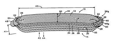
isolate predetermined layers coated on a substrate. Typically, as shown in Figs.1 and 2, the electrochromic device 10 in~ le~ a generally transparent substrate
12, such as an optical lens, and an edge isolation-contact system 14 mounted
WO95119588 215 81 6 8 PCT/IB9S/00121
thereon. Substrate 12 can be m~nnf~ctllred of glass, plastic or any other optical
material. Typically, as shown in Fig. 1, substrate 12 is a high-clarity optic lens for
use in non-prescription or prescription eyegl~cces. However, substrate 12 may bea camera lens, a window, a mirror, a clock face, a display or the like or an
electronic device. In many applications, the substrate typically will have a flat
edge, not a beveled edge as shown in the figures.
Light tr~ncmiccion through an EC cell, or EC device, is modulated
by moving ions in an electrochromic compound layer and a counter-electrode
layer by the application of an exterior bias voltage or potential difference between
first and second electrode layers which are positioned on opposite sides of the
electrochromic and counter-electrode layers. When all the layers of the device
are deposited on the substrate in an evaporator, a low resistance leakage path
typically will exist between the first and second electrodes in an edge region of
the substrate due to the thinnecc of such layers in the edge region. Thus, it isnecessary to provide a way of electrically connecting contacts to the first and
second electrodes, while ensuring that electrical isolation is m~int~ined between
the first and second electrode layers in the edge region to prevent a short circuit
or excessive current flow.
Fig. 2 is a cross section of device 10 shown in Fig. 1, taken along
line 2-2. As shown in Fig. 2, substrate 12 has applied thereon edge isolation-
contact system 14. Typically, substrate 12 incllldes a front surface 16, a rear
surface 18 and has a thicknesc 20. Front surface 16 is referred to herein also as
outer surface 16. Rear surface 18 is referred to herein also as an inner surface,
an expanse, or a generally flat region 18 of substrate 12. Substrate thi~necc 20is on the order of 2.0 millimeters (mm) for typical eyeglass lenses. Thi-~lrnesc 20
typically may be between 1.0 and 100 mm for camera lenses or between
approxi."~tely 1 to 6 mm for a plastic film. However, as is known by those skilled
in the art, such dimensions vary widely depending upon the use of substrate 12
and do not inhibit the effectiveness of system 14. Lens 12 further inchldes an
outer bevel region 22, an inner bevel region 24 and a bevel point 26. Bevel
regions æ, 24 and bevel point 26 are herein collectively referred to as edge
region, or perimeter, 26_.
WO 95/19588 215 8 1 6 8 pcTlIBssmol2l
Still referring to Fig. 2, system 14 typically inclll~les multiple layers
such as a first electrode layer 28, an intermediate electrochromic layer 30, and a
second electrode layer 32. Intermediate electrochromic layer 30 typically inclllcles
three sublayers 34, 36 and 38. Typically, thickness 41 of isolation-contact system
5 14 is on the order of 1-to-3 micrometers (~m), and is preferably appro~i"~tely1.5 ~m. Accordillgly, the drawings herein are not drawn to scale but instead areenlarged to show detail, with layer and coating thicknes~s greatly exaggerated.
As discussed in the co-pending application, the disclosure of which
is incorporated herein by reference, the typical EC device inclll(les first electrode
layer 28, intermediate electrochromic layer 30 and second electrode layer 32. Topower the electrochromic device, a potential difference is applied between firstelectrode 28 and second electrode 32. This difference in potential results in a
coloration and a change in the position of the electrical charge within the device,
also called a change in tr~n~mi~ivity of the lens, of interme~ te electrochromiclayer 30. Removing the potential difference between first electrode 28, which
typically is a cathode, and between second electrode 32, which typically is an
anode, results in a decolorization or "ble~ hing" of electrochromic layer 30. Thus,
controlling and holding a potential between electrodes 28 and 32 results in a
predetermined coloration of field of view 40 through substrate 12.
~or even coloration to take place in intermediate layer 30 across
field of view 40, an electrical cu~lenl must move between first electrode 28 andsecond electrode 32, generally in directions 42 and/or 44 through electrochromiclayer 30. Even thickness application of layers 28, 30 and 32 across expanse 18
enh~nces even shade coloration in field of view 40. Application of the layers
completely across field of view 40 and into edge region 26_ also permits even
coloration substantially throughout ffeld of view 40.
To ensure electrical current movement in directions 42 and/or 44
through intermediate layer 30, the first and second electrodes must be electrically
isolated in edge region 26_. Electrical contact between first electrode 28 and
second electrode 32 in edge region 26_ would result in a short circuit such thatcurrent passes through edge region 26a without the desired coloration or
ble~clling of electrochrornic layer 30. However, it is desirous to power device 10
WO 95/19588 _ 2 1 S ~ l tii 8 PCT/IB95/00121
by electrical connections to electrodes 28 and 32 in edge region 26a to m~ximi7efield of view 40 and to permit even thickness application of the layers on
substrate 12 throughout field of view 40. In addition, electrical contact in edge
region 26a places the contacts out of the field of view, enh~ncing the aesthetic5 appearance of device 10.
To achieve these dual functions, i.e. edge isolation between the
layers and simultaneous edge contact between a layer and an electrical contact,
preferably a dual conductive-nonconductive material system is provided.
Specifically, a first contact 46 is electrically connected to first electrode 28, and
10 a second contact 48 is electrically connected to second electrode 32. As discussed
in the co-pending application, contacts 46 and 48 are typically connected to a flex
circuit or other means of wiring and to a battery-operated power system that
controls and powers the device. An isolative barrier 50 typically extends
throughout perimeter 26_ and electrically isolates the first contact from the
15 second electrode layer and electrically isolates the second contact from the first
electrode layer.
Still referring to Fig. 2, first and second cont~ctc 46 and 48 may be
m~nnf~ctllred of any electrically conductive material, such as noble metals, andpreferably of a material incllltling gold ink. More specifically, the conductive20 material may be any metal which has no mobile ions. The preferred gold ink isa particle fflled, thermally curable polymer ink which cures at a low temperature,
such as 85 C. Gold ink is preferred due to its high electrical conductivity,
corrosion-resistant properties, and ease of application. Contacts 46 and 48 may
be applied by plating, soldering, pad printing, rolling, evaporation, brush
25 application, or by any other suitable process.
Isolative barrier 50 may comprise any dielectric material, and
preferably inchl~les lacquer. Preferably, the lacquer is a solventless, ultraviolet-
(W)-curable lacquer such as an epoxy acrylate or an organic resin. UV-curable
resins are preferred because such resins may be cured without olltg~csing of
30 solvents, which may harm the delicate layer system. W-curable resins also cure
more quickly than non-W-curable resins. This reduces the time between
beginning the curing process and beginning the next "pump down cycle" of the
WO 95/19588 2 ~. S 8 1 ~ ~ PCT/IB951On 121 ~
coating machine. ("Pump down cycle" refers to the time required to create a
vacuum pressure inside the coating m~chine to prepare the m~çhine for the next
co~ting process.) The lacquer may also be an urethane resin. Lacquer is
preferred due to its nonconductive properties, ease of application, aesthetics, and
5 low cost.
Still referring to Fig. 2, the process for m~nllf~ctllring the ~,refelled
electrochromic device comprises the following steps. First, substrate 12, typically
an optical substrate, is provided, having a generally planar expanse 18 and edgeregion 26_. First electrode layer 28 is then coated or applied to expanse 18 such
10 that the first electrode layer extends substantially across the expanse and into the
edge region. Preferably, first electrode 28 is coated on the entire surface of
expanse 18 such that first electrode 28 contacts and extends from bevel point 26on one side of expanse 18, across expanse 18, and thereafter contacts bevel point
26 on the opposite side of expanse 18. As disclosed in the co-pending application,
15 first electrode layer 28 and all subsequent layers may be applied to substrate 12
through spraying, vapor deposition, vacuum deposition or any like technique. Thetechnique may include physical deposition, plasma-assisted deposition, spray
pyrolysis, sol-gel deposition, screen printing or a physical and/or a chemical
deposition, such as sputtering and evaporation, the evaporation being either
20 thermal evaporation or electron beam evaporation.
These techniques produce a symmetric, even coating of the layer
across expanse 18 in a relatively straighLrolw~rd and cost-effective manner. In
addition, these coating methods coat expanse 18 subst~nti~lly across expanse 18
and into edge region 26_ such that the coating is evenly applied across the entire
25 field of view 40 of lens 12. M[ost often, these spraying and deposition te~niques,
as shown in Fig. 2, result in the layers "w~ h~g-around" bevel point 26. (This
"Wl~illg around" is only shown in Fig. 2 and is not shown in the other figures
for ease of underst~nding.)
In the second step of the process, first contact 46 is applied to first
30 electrode layer 28 along a signiffcant length in edge region 26a. As shown in Fig.
6, first contact 46 extends a significant length 52 along edge region 26~, whichmay be a~,ox;,.l~tely one-eighth of the perimeter 26_ of substrate 12. In
WO 95/19S88 ~ 1 5 81 6 ~ PCT/IB95/00121
addition, first contact 46 may be shorter or longer than one-eighth, and may have
a comb-like configuration inçln~ling teeth-like projections for çxtencling over the
thick edge region 26a of thick prescription lenses. These teeth-like projectionsare necessary for lenses having thick, or long, bevel regions bec~ e for good
S electrical connection first contact 46 preferably must contact a thick portion of
first electrode 28, which thins out along the beveled edge region. Applying first
contact 46 in edge region 26_ positions first contact 46 out of field of view 40 and
optimally positions first contact 46 along the substrate such that first contact 46
is hidden within an eyeglass frame when lens 12 is mounted in such a frame.
10 Applying contact 46 along a substantial length of perimeter 26a results in an even
potential distribution across expanse 18 which produces even shade coloration ofelectrochromic layer 30 and allows positioning of contact 46 such that it is
substantially or completely hidden from view within an eyeglass frame.
The third step in the process typically involves applying isolative
barrier 50 coll~hluously throughout edge region 26_ such that barrier 50 coats an
inner surface 46_ of first contact 46 along the length of first contact 46. In
addition, barrier 50 contacts edge region 26_ of substrate 12 and first electrode
28 from subsequently to-be-applied layers, continuously around the rest of
substrate 12. In this manner, barrier 50 electrically isolates first electrode 28
20 co.llill..ously throughout edge region 26_. As a further benefit of using a lacquer
isolation barrier, barrier 50 is typically thicker than the layers coated on thesubstrate so that the lacquer thickness compensates for any layer rollghn.os~ which
may result in an electrical short. For example, contact 46 may be comprised of
gold which has a very rough surface. The rough surface may penetrate through
25 subsequently applied layers, reslllsing in a short, if the lacquer was not used. The
thickness of the lacquer also may compensate for various shaped substrates whichhave various edge thicknesses or roughness.
To apply barrier 50, substrate 12 typically must be removed from
the coating m~chine that is used to apply the layer system. In the preferred
30 embodiment, the substrate must be removed only this one time, as opposed to
multiple removals required by prior art processes. Thus, the hlvellLive process
requires only one pump down cycle of the coating m~chine (in addition to the
WO 95/19588 PCT/IB95/00121 ~
2l58l68 10
first start-up "pump down cycle" required before processing begins), which savestime and money, m~kin~ the inventive process more efficient than prior art
processes. Specifically, after barrier 50 is applied, all four subsequent layers, i.e.
34,36,38 and 32, can be applied without removing the substrate from the coating
5 m~hine.
The fourth step in the process involves applying electrochromic
layer 30 to first electrode layer 28 such that electrochromic layer 30 extends
across the first electrode layer and into edge region 26a. In the preferred
embodiment, application of electrochromic layer 30 includes the sub-steps of
10applying layer 34 to first electrode 28, thereafter applying layer 36 to layer 34, and
thereafter applying layer 38 to layer 36. Electrochromic layer 30 is preferably
evenly coated on first electrode 28 such that electrochromic layer 30 extends
across first electrode 28 and contacts barrier 50 throughout edge region 26_ while
first electrode 28 physically isolates electrochromic layer 30 from substrate 12.
15The fifth step in the process comprises applying second electrode
32 to electrochromic layer 30 such that the second electrode layer extends across
the electrochromic layer and into the edge region. Preferably, second electrode
layer 32 contacts barrier 50 along the barrier's length. In this arrangement, the
electrochromic layer physically isolates the second electrode from the first
20 electrode.
All layers are evenly coated across substrate 12 such that there is
an even thickness 41 generally throughout field of view 40. Such an even,
symmetrical coating of layers 28, 30 and 32 results in a structure that produces a
resistance between electrodes 28 and 32 that is even throughout field of view 40.
25 This even coating of all layers throughout field of view 40 is made possible
because the interconnect-isolation barrier system is located outside field of view
40 and in edge region 26_.
The last step in the process of m~nllf~ct. lring the electrochromic
device comprises applying second cont~ct 48 to the second electrode layer 32
30 along a significant length 52, applox;",~tely one-eighth of the entire length of
edge region 26_. However, the contact may be as long as approx;~ tely seven-
eighths of the entire length. Typically, second contact 48 is positioned generally
~ WO 9~/19588 21 5 81 6 8 PCT/IB9~/00121
11
opposing first contact 46 across expanse 18, as shown in Fig. 6. Opposite
positioning of contacts 46 and 48 may help create an even potential difference
between first electrode 28 and second electrode 32, which results in even
coloration of electrochromic layer 30. Opposite positioning also reduces the
possibility of a short circuit. Furthermore, remote positioning reduces the bulkof system 14 in a single region of edge region 26_ so that lens 12 may be easilyplaced in an eyeglass frame. A stacked, adjacent positioning of the contacts maybe desirable to hide contacts 46 and 48 within a frame when the frame only
covers a portion of the lens perimeter, such as sports lenses wherein the frame
only covers the top portion of a single long lens covering both wearer's eyes. This
process described above results in an EC device whereby an electrical charge maybe applied across EC layer 30 resulting in the desired coloration of the device and
minim~l electrical charge leakage in the edge region.
Electrochromic device 10 may further include protective layers
coated on second electrode 32 to protect the device from normal wear and tear
such as abrasions, weather elements, ultraviolet degradation or other damage.
The additional protective layers, which are not shown in the drawing, may inclllde
a buffer layer, a scratch-resistant layer, an anti-reflective layer or a hydrophobic
layer.
The lacquer isolation-interconnect process just described avoids the
use of mechanical or chemical masks that would be required in a mechanical or
chemical isolation-interconnect system. Such masks can make m~nnf~ctllre of an
EC device fin~n~ lly prohibitive hecause a multitude of different masks is needed
for various optical lens prescriptions, lens shapes, and even for left and rightlenses.
Shown by the second embodiment in Fig.3, a second m~n~lf~ctnring
process is described below. First, substrate 12 is coated with a first inllillm tin
oxide (lTO) layer 28 which extends across back surface 18 of substrate 12, into
edge region 26_ and over bevel point 26. This first layer 28 comprises the bottom
electrical contact layer. Second, after removing substrate 12 from the coating
m~cl~in~, first contact 46, preferably inclll(ling gold ink, is applied in edge region
26_ over first electrode 28 such that the gold ink extends over bevel point 26 and
2158168
WO 95/19588 _ PCT/IB95/Q0121
12
beyond the first electrode coating. The gold ink is therrnally cured at 85 C for
~r-~xi,,,~tely 7 to 10 minlltes Once cured, the gold ink provides a first contact
46 along a significant portion, preferably one-eighth of the perimeter 26~, of the
device. Third, a ffrst strip of m~Cl~ing tape is placed over the gold ink in edge
5 region 26~, the m~cking tape extending over bev~point 26 and beyond the gold
ink such that the m~Cl~ing tape extends onto the front surface of substrate 12.
Now, the substrate is ready for application of the rem~ining layers.
Still referring to Fig. 3, the fourth step inclllrles, after placing the
substrate in the coating m~çhine, successively coating a tungsten oxide (WOx)
layer 34 and an in~nl~tive layer 36 across surface 18, both of which extend intoedge region 26_. Specifically, the WOx layer 34 and in~ tive layer 36 extend
up to or onto the gold ink layer 46 and over the first strip of m~king tape (notshown). Typically, the in~ tive layer is lithillm ~I"",i"ll", fluoride (~iAlF), also
referred to as "AI~". Fifth, after removing substrate 12 from the coating
15 m~chine, a continuous bead of lacquer 50 is coated throughout perimeter 26_
such that the lacquer extends over bevel point 26. Lacquer bead 50 p~ve~
electrical shorts between the first and second electrodes of the device. Sixth, after
placing substrate 12 into the coating m~t~hine, a v~n~ lm oxide (VOx) layer 38
and then a second ITO layer 32 are coated on surface 18 such that the layers
20 extend into edge region 26_.
In this embodiment, as will be realized by those skilled in the art,
electrical contact between WOX layer 34 and VOX layer 38 across in~ tive layer
36 would create an electrical short. Thus, those skilled in the art will realize that
throughout the spe~ific~tion, edge-wise electrical contact or isolation between the
25 first and second electrode layers will also be understood to mean edge-wise
electrical cont~ct or isolation between plural layers at least one of which is
opposite the other across in~ tive layer 36. Those skilled in the art will also
realize that the multi-layer system coated on substrate 12 may comprise organic
or inorganic layers, or a ll~ixlule of organic and inorganic layers. After the sixth
30 step, the device is ready for application of the insulative lacquer.
Still referring to Fig. 3, it may be seen that the seventh step
inclll~les, after removing the substrate from the coating m~rhine, applying
~ WO 95/19S88 215 816 8 pcTlIBsslonl2l
13
in~ tive lacquer 50 along edge region 26~, preferably opposite the edge region
of first contact 46. The lacquer preferably is applied throughout edge region 26~
but may also be applied only along a portion of the edge region. Fi~hth, a second
gold ink layer 48 is applied in edge region 26~, generally over the second lacquer
S layer but in contact with second electrode 32, and generally opposite ffrst contact
46. Ninth, a second strip of mA~king tape is positioned over gold ink 48. Tenth,after placing the substrate in the coating m~rhine, an organic or inorganic coating
(not shown) is coated over the second ITO layer 32. The overcoat layer may be
parylene-C, UV-curable urethane, or silicone dioxide. The organic or inorganic
overcoat layer acts as an environmental barrier, protecting inner layers from
environmental damage to the EC device. Eleventh, after removing the substrate
from the coating m~çhinç, the ffrst and second strips of m~king tape are removedto expose ffrst and second contacts 46 and 48. Twelfth, after placing the substrate
in the coating mAçhine, a spin hard coat, also called a spin coat, is applied over
the previously coated layers to protect the surface from physical abrasions and
damage. Lastly, after removing the substrate from the coating m~chine, a third
lacquer barrier is applied co~ llously throughout edge region 26a to protect theperiphery of the device and to avoid electrical shorts between the second ITO
layer 32 and a metal frame.
AnotherlllAllllrAct~lringprocessisdescAbedbelow. First,substrate
12 is coated in edge region 26a with a ffrst release agent. The ffrst release agent
is coated generally throughout edge region 26_ but leaving a ffrst exposed region
uncoated. Typically, the first release agent is coated continuously along 7/8 ofthe perimeter 26~, leaving 1/8 of the perimeter exposed. The release agent
typically extends from bevel point 26 onto back surface 18 the same cli~t~nce asffrst contact 46 extends from bevel point 26 onto back surface 18 such that the
contact and the layer are subst~ntiAlly coextensive. Typically, the first release
agent is an agent which adheres to the substrate but which subsequently applied
layers do not easily adhere to. In addition, the first release agent must be easily
removable from the substrate by washing or by peeling the first release agent off
the substrate. Typically, the ffrst release agent is a ~ re of one percent by
volume soap and ninety-nine percent by volume water. The release agent may
WO 95/19588 2 ~ 5 g 1~ 8 PCT/IB95/00121 ~
14
also be tape, a low adhesion material, such as a silicon polymer which is painted
on the substrate, or ink, such as found in a typical felt tip pen.
In the second step, the first electrode layer 28 is coated across
substrate 12 and extends into edge region 26_ such that the first electrode layer
5 extends onto the first release agent and into the first exposed region of perimeter
26_. Third, the first release agent is removed from substrate 12 thereby removing
the portion of the first electrode layer which was coated on top of the first release
agent. Where the first release agent is soap, the release agent can be removed
by washing. Where the firs~ release agent is tape, the release agent can be
10 removed by merely peeling the tape off substrate 12. Fourth, edge region 26_ is
cleaned, preparing the edge region for subsequent layer deposition.
Fifth, a second release agent is applied in edge region 26_ such that
the second release agent çxten~l~ generally throughout edge region 26_. Typically,
the second release agent extends continuously throughout 7/8 of edge region 26a
15 leaving exposed 1/8 of edge region 26~, also called a second exposed region. The
second exposed region is typically located opposite the first exposed region, across
substrate 12. Sixth, intermediate electrochromic layer 30 is applied such that
intermediate layer 30 generally coats electrode layer 28 across substrate 12.
Typically, intermediate layer 30 is applied such that the layer extends into edge
20 region 26a and onto the second release agent, and also into the second exposed
region. Seventh, second electrode layer 32 is coated onto intermediate layer 30.Typically, the second electrode layer extends into edge region 26~ thereby
cont~cting the second release agent. F.ighth, the second release agent is removed
from edge region 26a. Ninth, edge region 26_ is cleaned to remove any residue
25 from the second release agent.
In the tenth step, first contact 42 is applied in the first exposed
region, and second contact 48 is applied in the second exposed region, such thatthe first and second contacts are located generally opposite from one another
across substrate 12. Lastly, a protective overcoat is applied to the substrate
30 thereby protectively coating the underlying multi-layer system, but leaving exposed
the first and second cont~ctc. Use of this multi-release agent process results in
an edge isolation-contact system whereby an electrical charge may be applied
~ WO 95/19588 21 5 g I ~ 8 pcTlIBsslonl2l
across electrochromic layer 30 resulting in the desired coloration of the deviceand minim~l electrical charge leakage in the edge region.
Yet another m~nllf~tllring process is described below. First, a first
release agent is applied in edge region 26_ such that the first release agent
5 extends throughout seven-eighths of edge region 26_, thereby defining a first
exposed region. Second, the first electrode layer is coated on substrate 12 suchthat it extends across substrate 12 and into edge region 26_, cont~cting the first
release agent. Third, the first release agent is removed thereby removing the
portion of the first electrode layer coated on top of the first release agent and
10 leaving the portion of the first electrode layer which is in the first exposed region.
Fourth, the edge region 26_ is cleaned, removing residue of the first release
agent.
Fifth, a second release agent is applied in edge region 26~, and
typically extending around 1/8 of perimeter 26_. Preferably, the second release
15 agent is applied in the first exposed region. The second release agent must be
applied such that it overlaps the first electrode layer to create the desired
isolation-contact system. Sixth, intermediate layer 30 is coated on substrate 12thereby cOve~ing the first electrode layer and extending onto the second releaseagent. Seventh, the second release agent is removed, thereby removing the
20 portion of intermediate layer 30 coated on the second release agent. Fighth, edge
region 26_ is cleaned to remove residue of the second release agent.
Ninth, a third release agent is applied generally throughout edge
region 26_ such that the third release agent extends al~ploxi~ tely seven-eightsof the distance around edge region 26~, defining a second exposed region which
25 is located generally opposite across substrate 12 from the first exposed region.
Tenth, second electrode layer 32 is applied to substrate 12 such that the secondelectrode layer covers the intermediate electrochromic layer and extends onto the
third release agent. Eleventh, the third release agent is removed from edge
region 26 . Twelfth, the edge region is cleaned to remove the residue left from
30 the third release agent.
In step thirteen, a contact is applied in the first exposed region and
a second contact is applied in the second exposed region, which are typically
WO 95/19588 21 S 816 8 pcTlIBssmol2l ~
16
located opposite one another across substrate 12. Lastly, a protective overcoat
is applied to the substrate thereby protectively coating the underlying multi-layer
system, but leaving exposed the first and second~contacts. Use of this multi-
release agent process results in an edge isolation-contact system whereby an
electrical charge may be applied across electrochromic layer 30 res~llting in the
desired coloration of the device and minim~l electrical charge leakage in the edge
reglon.
In a second embodiment, shown in Fig. 3, first electrode 28 is
coated on expanse 18. First contact 46 is then coated along a ~ignific~nt length52 of edge region 26a, thereby contacting bevel point 26 and first electrode 28.Thereafter, sublayer 34 and sublayer 36 of electrochromic layer 30 are coated onfirst electrode layer 28. Barrier 50 is then coated continuously throughout edgeregion 26a such that barrier 50 contacts first contact 46 along its length, and
thereafter contacts substrate 12 and sublayer 36 throughout the rest of edge
region 26~. Sublayer 38 of electrochromic layer 30 and second electrode 32 are
then sequentially coated onto sublayer 36. Next, second contact 48 is coated on
barrier 50 and second electrode 32 along a significant length 52 of edge region
26_, generally opposite first contact 46 across substrate 12.
The embodiment shown in Fig. 2 is preferred over the embodiment
shown in Fig. 3 because as shown in Fig. 2, layers 34, 36, 38 and 32 are all
sllcces~ively coated on substrate 12 without removing the substrate from the
coating m~hine. In contrast, the device shown in Fig. 3 must be removed from
the coating m~chine after application of layer 28 and after application of layers
34 and 36, and subsequently replaced back into the coating m~chine for the finalcoating of layers 38 and 32. Thus, to m~mlf~ctllre the device of Fig. 3, two
additional pump down cycles are required whereas only one pump down cycle is
required to m~nllf~c~lre the device of Fig. 2. In another embodiment similar to
the one shown in Fig. 2, contact 46 may be applied directly to substrate 12, such
that the process only requires one pump down cycle in addition to the original
pump down cycle.
Those skilled in the art will realize that the release agents may be
removed at other various stages in the process to achieve variations of the recited
~, WO95/19588 21 S 81 6 8 PCT/IB95/00121
17
processes.
Electrochromic device 10 can also be thought of as a transparent
substrate 12 having an edge region 26_, and a generally flat surface 18. The
device may further comprise an electrochromic layered structure 14 positioned on5 the flat surface, and at least partially overlapping, edge-applied, conductivematerial 46, 48 and in~ tive materials 50. These in~nl~tive materials provide
layer-selective conductive and in~ tive edge-contact for edge-wise electrical
power input to the device. Layer-selective conductive and in~ tive edge-contact
means that predetermined layers may be contacted by a cont~ct while other layers10 are not contacted and are in~ ted from the contact. The con~l~lctive and
in~nl~tive materials are positioned out of a field of view 40 through the
transparent substrate, which m~ximi7:es the field of view 40 and gives a pleasing
aesthetic appearance to the device.
Fig. 4 shows a third embodiment wherein layers 28, 34, 36, 38 and
32 sequentially are coated on substrate 12 without removing substrate 12 from the
coating machine. In this embodiment, only the original pump down cycle is
required. Thereafter, the solid-state electrochromic device, meaning substrate 12
and the applied layers, is removed from the coating m~hine. After removal of
the device from the coating m~chine, an edge-isolation channel 52 is formed in
20 edge region 26a effectively to electrically isolate first electrode layer 28 from
second electrode layer 32 in field of view 40. Edge-isolation channel 52 therebyinhibits a short circuit from occurring in the field of view of the device by
electrical contact between first and second layers 28 and 32 while ch~nnel 52
permits controlled contact of a potential to such layers to power the device. As25 will we re~li7e-1 by those skilled in the art, channel 52 need only penetratethrough insolative layer 36 to be effective. Nonconductive material 50 may be
applied to the channel to protect the channel from damage. Typically, channel
52 extends through predetermined layers, specifically, through second electrode
layer 32 and into electrochromic layer 30. Preferably, channel 52 is formed by
30 use of a laser which allows precision depth cutting into electrochromic layer 30.
However, channel 52 may be formed by any method, incl~ltling use of wet
chemistry, dry chemistry or mechanical abrasive removal of selected upper layers.
WO 95/19588 21~ 81~ 8 PCTIIB95/00121 ~
18
As shown in Fig. 4, first contact 46 and second contact 48 are each
applied in edge region 26a along a substantial length of perimeter 26_. The
contacts are typically positioned opposite substrate 12 from each other. First
electrode layer 28 can receive a positive electrIcal charge, and second electrode
5 layer 32 can receive a negative electrical charge, or vice versa, creating a potential
difference through electrochromic layer 30, without first and second electrodes 28
and 32 short circuiting in edge region 26a.
Still referring to Fig.4, typically the multi-layer coating on substrate
12 is oriented parallel to a first plane 12a, defined generally by back surface 18
10 of substrate 12 (which it will be understood typically is slightly curved). Ch~nnel
52 is typically oriented parallel to a second plane 52~, the second plane being
oblique relative to the first plane defined by the multi-layer coating. Preferably,
the second plane 52_ defined by channel 52 is subst~nti~lly normal to the first
plane 12a defined by the multi-layer coating.
After trench, or channel, 52 is cut into the multi-layer coating, first
contact 46 is applied along a substantial length of the multi-layer system in edge
region 26a. Due to the relatively small thickness of the layers in edge region 26~,
second electrode 32 may be electrically connected to first electrode 28 in edge
region 26_. However, channel 52 ~rt;vellls a short in the edge region from
20 creating a short in field of view 40. Thus, using the short in edge region 26a as
an advantage, first contact 46 may be applied to first electrode 28 or to secondelectrode 32 in edge region 26a to electrically connect with first electrode 28 in
the edge region.
If channel 52 is not filled with a nonconductive material, contact 46,
25 when applied, may inadvertently be applied into channel 52. If first contact 46
is applied in to channel 52, it may create a contact between the first and the
second electrodes. Such contact would create an electrical short and therefore
result in a non-flmction~l EC device.
To remedy this problem, after application of first contact 46, barrier
30 50, which typically includes lacquer, is coated along edge region 26a such that
barrier material 50 fills channel 52 along the length of co~t~ctc 46 and 48. In this
channel embodiment, barrier 50 acts merely to fill channel 52 with a
~ WO 9S/19588 215 81 6 8 PCT/IB95/00121
19
nonconductive material, and prevents contact materials 46 and 48 from being
applied into channel 52, which would circumvent the isolative purpose of channel52. Thus, in this embodiment, channel 52 itself electrically isolates first electrode
28 from second electrode 32 so that barrier mateAal 50 need not extend
5 completely around perimeter 26_ but merely the length of the contacts.
Preferably, barrier 50 does extend conli-luously around edge region 26_ to protect
channel 52 from the weather elements and other types of damage. In addition,
barrier 50 preferably extends throughout perimeter 26_ to prevent an electrical
short when device 10 is placed in a metal frame.
10As shown in Fig. 4A, a second trench 54 may be formed in edge
region 26_, generally adjacent trench 52 to facilitate contact of first contact 46 to
first electrode 28. This embodiment avoids using a short in edge region 26_ to
contact first electrode 28 with first cont~rt 46. Whereas trench 52 extends
continuously around perimeter 26_ to isolate first electrode 28 from second
15electrode 32 in field of view 40, second trench 54 only need extend a limited
distance along perimeter 26~, preferably, the same length as contact 46.
Typically, second trench 54 is formed through use of a laser and
extends through second electrode 32 and into intermediate layer 30. Thereafter,
second channel 54 may be exposed to a chemical etch or removal process so that
20the finished second channel 56, shown in Fig. 4B, extends down to, and exposes,
first electrode 28. Contact 46 is then applied in to channel 56 such that contact
46 directly electrically contacts first electrode 28.
In the preferred embodiment, layer 28 is ITO, layer 34 is an
electrochromic compound, layer 36 is an electrolyte, layer 38 is a counter-
25electrode, and layer 32 is another layer of ITO. Preferably, second ~nnel 54 is
cut through layer 32 and into layer 30, i.e., into 34, 36 or 38.
Thereafter, as shown in Fig. 4B, a basic pH solution, such as a
sodium hydlo~ide chemical etch, is used to expose layer 28, shown as finished
second channel 56. The sodium hydroxide solution is used because it chemically
30etches, or removes, layers 34, 36 and 38 but will not etch through lTO layers 28
or 32. Thus, layer 32 acts as a mask ~revel~h~g enlargement of channel 54 and
layer 28 is fully exposed to, but not etched by, the sodium hydroxide. Use of this
2l58l68
WO 95/19S88 ^ PCT/IB9~/00121
combined laser/chemical etch process to first make channel 54 and then to finishit into a deeper finished channel 56, fully exposes first electrode 28 for contact
with first contact 46, while not subjecting the delicate electrochromic layers 30 to
more than one chemical etch. Furthermore, the laser/chemical etch formation
of second channel 56 does not require use of a separate mask for second
electrode 32 but instead uses second electrode 32 itself as a mask because it isnot etched by sodium hydroxide. Thus, this process lowers the cost of producing
the EC lens because a separate mask is not needed for each different prescription
and shape of lens used. The process results in an EC device whereby an
10 electrical charge may be applied across EC layer 30 resnlting in the desired
coloration of the device and minim~l electrical charge leakage in the edge region.
Another method of achieving edge-wise isolation-contact comprises
coating a first contact 46 in an edge region 26 of substrate 12 along a significant
length. The substrate is then placed in the coating m~hine for application of all
15 layers. Thus, this process requires no additional pump down cycle other than the
initial pump down cyde needed to prepare the coating m~chine. A channel 52
is then formed in the edge region, electrically isolating the first and second
electrode layers in the field of view. Due to the thickness and ro~lghnes~ of first
contact 46, typically gold ink, first contact 46 will have areas which extend
20 outwardly and through the thin subsequently coated layers. Thus, the first
electrode can be contacted through the edge region short circuit created by first
contact 46 projections which electrically connect all the layers in the edge region.
An insulative layer can then be applied along a signifi~ ~nt length to allow second
contact 48 to be connected to the second electrode layer.
In another embodiment, direct electrical contact can be made
between the flex circuit and the first, or second, electrode without the use of first,
or second, contacts, respectively. Such an embodiment may involve me~h~ni~l
pressure, in the case of eyewear, such as tightly ~lhll~ g the frame about the lens,
in the case of eyewear, which forces the flex circuit into contact with the
30 ay~rol,liate electrode layer.
Figs. S and 6 show front and back elevational views, respectively, of
the preferred embo-liment
WO 95119588 21~ 8 PCT/IB95/00121
21
In another embodiment, the device may comprise the use of
in~ tive material and a channel which work in combination to permit electrical
isolation and interconnection between layers coated on a substrate. Specifically,
the device may comprise a substrate having an edge region and a generally flat
surface. The device may further comprise an electrochromic layered structure
located on the generally flat surface and an edge-applied in~ul~tive material atleast partially overlapping with the layered structure. The device may also
co~ lise a channel formed in an edge region of the electrochromic layered
structure, the in~nl~tive material and the channel together providing layer-
selective insulative edge-contact in the edge region for edge-wise electrical power
input to the device. The device may also further comprise edge-applied
conductive material.
Thus, the device may include edge-applied in~nl~tive material, edge-
applied conductive material, a channel, or a combination thereof, to achieve thedual purpose of edge-wise electrical isolation and interconnection of the layers.
The in~ tive material, the conductive material, the channel, or any combination
thereof is herein referred to as an isolation mech~ni~m Thus, the particular
isolation me.~h~ni~m chosen results in electrical isolation and yet permits
interconnection of a~L,r~liate layers of the monolithically layered system.
As shown in Fig. 7, the invention further comprises a process and
a device 57 for applying coating material, such as first or second contacts 46 and
48 or preferably barrier 50, to the perimeter of an eccentric substrate, the process
comprising the following steps. First, a substrate 12 is provided having a generally
flat expanse 18 bounded by an eccentric perimeter 26_. For example, eccentric
substrate 12 may be a noncircular substrate or an eccentrically mounted circularsubstrate. The substrate has a substrate axis 58 through a central region of theexpanse. Substrate axis 58 is typically normal or perpendicular to the generallyplanar surface of expanse 18.
Next, substrate 12 is mounted, through use of an adhesive 61 or the
like, to a rotary motor 60 which rotates the substrate about substrate axis 58 such
as in direction 60a. Typically, substrate 12 is mounted to rotary motor 60 on the
terminal end of its rotating spindle or shaft.
%ls8~8
WO 95/19588 PCT/IB95/00121 (~
Rotary motor 60 is connected to a linear motion me~h~ni~m 62, the
linear motion mech~ni~m moving the motor 60 and the mounted substrate 12 in
a line 64 generally perpendicular to substrate axis 58. Typically, linear motionmech~nicm 62 comprises a simple pulley system which is counterweighted such
5 that minim~l power is required to move substrate 12 and rotary motor 60 along
line 64.
Next, a coating material 50 is applied to a roller mech~ni~m 66.
Roller me~h~ni~m 66 typically inçllldes one roller 66_ but may inf hl(1e dual rollers
66a and 66h operatively associated with one another. Roller 66_ and roller 66b
rotate in directions 68 and 70, respectively, thereby spreading coating material 50
over an upper surface 66c of roller 66_. Roller 66a is typically positioned
generally adjacent the perimeter 26a of substrate 12 when the substrate is
mounted on rotary motor 60.
Still referring to Fig. 7, to coat lens perimeter 26a of substrate 12
with coating material 50 on roller 66~, substrate 12 is rotated in direction 60a by
rotary motor 60. At the same time, the substrate is moved linearly along line 64by linear motion me~h~ni~m 62 such that perimeter 26a continuously contacts
coating material 50 at a region 665~ on roller 66_. As substrate 12 is rotated
about substrate axis 58, perimeter 26a and roller 66a have the same velocity at
contact region 66d such that coating material 50 is evenly coated on perimeter
26a of substrate 12. As will be understood by those skilled in the art, effecting
relative motion between the substrate and the coating material to be applied will
produce the desired result. Thus, in another embodiment, the substrate may be
held stationary as the adjacent mech~ni~m~ are moved.
Typically, substrate 12 is an eyeglass lens having an outer bevel 22,
an inner bevel 24 and a bevel point 26, shown in Fig. 7A (which is a fragmentarydetail of area A of Fig. 7). To achieve an even coating of material 50 on edge
region 26a two angles, namely ~1 and ~2 are of importance.
Referring again to Fig. 7, a1 represents the angle between upper
surface 66_ of roller 66_ and a baseline, typically the horizontal, represented by
line 72. Material 50, which is applied to roller 66~, tends to flow dowllw~rdly
along snrf~e 66c due to gravity. As ~1 is increased, material 50 tends to flow
~ WO 95/1958~ 215 816 8 PCT/IB95/00121
23
more quickly. As the flow speed increases, more material tends to wick up onto
the perimeter 26_ due to surface tension, coating a larger portion of the
perimeter. Controlling ~l controls the amount of this wicking of material 50 onto
substrate 12.
As shown in Fig. 7A, ~2 represents the angle between inner bevel
24 and surface 66c. Varying ~2 determines the bevel surface of lens 12 to which
material 50 is applied. Specifically, as ~32 iS increased, the wicking action ofmaterial 50 along inner bevel 24 is decreased due to surface tension, and the
wicking action of material 50 on bevel point 26 and outer bevel 22 is increases.As ~2 approaches 0, the wicking action of material 50 tends to coat only inner
bevel 24. As fl2 becomes negative, meaning that only edge 24_ near inner bevel
24 contacts material 50 and that bevel point 26 is lifted up off edge 66c, the
wicking action of material 50 tends to coat only inner bevel 24 and does not coat
bevel point 26 or outer bevel 22.
Controlling the rate of application of material 50 to roller 66~L, angle
~" angle ~2, the rotary speed of substrate 12 created by rotary motor 60, and the
linear motion of substrate 12 created by linear motion mech~ni~m 62, all vary the
location and thickness of coating 50 applied to edge region 26_. Other factors
which may iniluence the application of material 50 to substrate 12 inclll-le theviscosity of material 50, the composition of the material, the distance between
rollers 66_ and 66k which inflllençes the thicknes~ of material 50 on surface 66_,
and the temperature of the coating procedure.
As shown in Fig. 8, another embodiment of a device 74 for applying
coating material 50 to edge region 26_ includes a rotary motor 76 having an arm
78, the length of which is the same as the radius 78_ of substrate 12 measured
from a pivot point, or focal point 76_ to the outer surface 16 of substrate, or what
may be referred to now as a lens, 12. Arm ?8 rotates substrate 12 about substrate
axis 58 in direction 60a while moving substrate in direction 80. Direction 80 isa curving motion which defines a circular arc of radius 78_ of the outer ~;Ul v~Lure,
also called a base, of eyeglass substrate 12. Stated another way, swing arm 78 is
the same length 78_ as the outer radius 78_ of substrate 12 measured from focal
point 76_ to the outer surface 16 of the substrate. In this manner, as swing arm
WO 95/19S88 21 S ~ 1 ~ 8 PCT/IB95/00121 1--
24
78 rotates substrate 12 in direction 60~ about axis 58, and ~imlllt~neously moves
substrate 12 in direction 80, contact point 66_ remains in contact with surface 66c
of roller 66a. In this manner, an even coating of material 50 is applied to
perimeter 26~, regardless of the shape of substrate 12. This application processis particularly useful for applying barrier mat-è~ial 50 to an eyeglass lens having
an eccentric perimeter or a circular lens which is eccentrically mounted on device
74. While not shown in Fig. 8, such~pivotal arrangement may also be counter-
weighted.
In another way of describing the invention, the invention comprises
10 a device for applying coating material to the perimeter of an eccentric optical
lens, the lens having a lens axis generally orthogonal to its generally planar
expanse. The device comprises a rotary motor adapted for mounting a lens on
the motor, the motor structured to rotate the lens about the lens axis. The device
also comprises a linear motion mech~ni~m connected to the rotary motor, the
15 linear motion mech~ni~m moving the rotary motor in a direction generally
perpendicular to the lens axis when the lens is mounted on the rotary motor. Thedevice further comprises an applicator positioned generally adjacent a perimeterof the lens when the substrate is mounted on the rotary motor. The linear motionmech~nicm and the applicator mech~ni~m are operatively associated such that the
20 linear motion mech~ni~m moves the lens as the rotary motor rotates the lens such
that the lens contacts the applicator mech~ni~m at a fixed point. In other words,
the linear motion mech~ni~m and the rotary motor move the lens relative the
applicator so that the perimeter of the lens, or substrate, contacts the applicator
mech~ni~m at the same point on the applicator mech~ni~m as the lens is rotated.
As shown in Fig. 9, the invention further comprises conductive pads
82 to effect an electrical contact between electrochromic device 10 and a
conductor 84, such as a flex circuit (which is connected to a power drive circuit,
not shown), the conductor and the circuit controlling and powering device 10.
Specifically, device 10 is shown with first contact 46 (the multi-layer system not
30 being shown for clarity) located generally within the recess 86 of an eyewear lens
frame 88. Those skilled in the art will realize that frame 88 may be a camera
lens frame, a mirror frame, a window frame, or the like and may be one of a
WO95/19S88 ~ 15 81 6 8 PCT~B95/00121
variety of cross-sectional shapes. In addition, those skilled in the art will realize
that direct contact may be made between the flex circuit, the elastomeric pad, and
the a~3~ropliate electrode layer without use of a contact 46 or 48.
Preferably con(lllctQr, or lens-cont~ting region, 84 iS formed of
5 gold-plated copper, therèby to ensure reliable electrical contact and to reduce the
tendency of the copper to corrode, especially under more severe ellviro,mlental
conditions. Elastomeric conductive strip or pad 82 iS located between conductor
84 and first contact 46, pad 82 resiliently eYr~ntling or being colll~ressed to fill
the gap between flex circuit conductor region 84 and first contact 46. Those
10 skilled in the art will realize that such elastomeric conductive strips 82 may also
be used to connect a second contact 48 (not shown) to a second conductor region
of the flex circuit. Typically, pad 82 iS an anisotropic connector sheet, such as
"Shin-Flex MAF-Connector", available from Shin-etsu Polymer Arnerica, Inc.
Preferably, pad 82 iS m~nnf~ct~lred by providing corrosion-resistant conductive
15 filler material such as nickel particles, gold particles, or carbon or gold-coated
nickel particles within an elastomeric material. The conductive filler materialscan be in the form of needles, random particles, or flakes, so long as they provide
thickness-wise conductivity through pad 82.
Still referring to Fig. 9, when the elastomeric pad 82 iS colllpressed
20 by pressure between substrate 12 and frame 88, the cQnclllcffve particles co~t~ct
one another thereby creating an electrical path through the elastomer pad 82. Inanother embodiment, the cQnclllçtive filler materials may be generally needle-
shaped deffning an electrical path from one side of the pad to the other, e.g.
extending from contact 46 to conductor 84. The elastomeric material used to
25 m~nllf~ctllre pad 82 may be silicon, rubber or the like. Preferably, tacky silicon
is used such that pad 82 has adhesive properties which make it easy to adhere pad
82 to contlllçtor 84 or to contact 46.
In another embodiment, pad 82 may comprise metal powders mixed
in a slurry with silicon caulk, or a solder paste, which is then cured. In yet
30 another embodiment, pad 82 may be m~nllf~ctllred directly on conductor 84 by
a silk screen process. Silk screening pad 82 directly onto the collductQr 84 saves
labor by reducing the ~ --lr~çtllring step of adhering pad 82 to conllllçtor 84. In
WO 95/19588 ~15 81~ 8 PCT/IB9;S/00121
26
another embodiment, pad 82 can be m~nllf~3ctured directly on contacts 46 or 48.
In yet another embodiment, conductor 84 may be a wire and pad 82 may be
m~nl7f~ctnred directly around wire 84, e;g;, as part of an extrusion or rolling
process. .~ '
Pad 82 has the additional beneffts of preventing shock to device 10
such as physical shock, thermal shock, vibrational shock and cont~min~tion by dirt
or moisture. In addition, the resilient properties of pad 82 allow for greater
tolerances in m~mlf~cturing a system incorporating electrochromic device 10.
Specifically, in the case where electrochromic device 10 is a pair of prescription
10 optical glasses, each substrate 12 is a hand-ground lens having a specific shape to
fit a speciffc eyeglass lens, and a width determined by the eyeglass prescription.
Due to these numerous variables, producing an eyeglass lens having a multi-layerelectrochromic system coated thereon, may not fit perfectly within the chosen
eyeglass frame. Such an imperfect fit may result in a poor electrical contact
15 between a contact, such as contact 46, and its respective conductor such as
conductor 84. Use of elastomeric pad 82 increases the tolerance of the system byproviding a resilient and flexible electrical connection path.
In another embodiment, the multi-layer isolation-interconnection
EC system can be used as a super-capacitor. In other words, the isolation-
20 interconnect system, which provides for electrical current flow in directions 42 and
44 through a central region of the layered device, may be used as an electrical
component in an electrical system. In such an embodiment, the aesthetics of the
device will typically be imm~terial, as will the optical properties. For example,
one may replace the transparent conductive indium tin oxide with a metal, such
25 as ~lln~ or gold.
The invention also comprises a process of efficiently mass producing
electrochromic devices, such as windows or ll~illol~. The process involves the
following steps. First, a substrate is provided which incln~les an expanse. The
expanse may be a long sheet of glass or a coll~hluous sheet of glass fed directly
30 from a glass sheet m~mlf~ctllring process. Coatings are then applied generally
across the expanse. Specifically, a first electrode layer, then an intermediate
electrode layer, then a second electrode layer are coated on the expanse. The
21581~8
~`1 WO 95/19588 PCT/IB9~/00121
27
substrate is then physically divided into sections having a central region.
Preferably the sections are standard-shaped windows or mirrors. In addition, odd-
or custom-shaped sizes may be cut from the substrate. The cut and separated
section will have a central region and an edge region, or perimeter, extending
5 completely around the section. A channel is then formed in the edge region of
the separated section to electrically isolate the layers in the central region. An
electrical contact is connected to the first electrode and another electrical contact
is connected to the second electrode in the edge region to complete m~nnf~ctllreof the electrochromic device.
The benefits of this process allow large substrates to be coated and
thereafter physically cut to speciffed dimensions. This process decreases pump
down cycles of the coating m~chine. In addition, the substrate can be stored andphysically cut at a later time which decreases the cost and time required to
m~nnf~cture custom-sized sections, e.g. window panes, for use as electrochromic
15 devices.
While the present invention has been shown and described with
refere"ce to the foregoing preferred embodiment, it will be apparent to those
skilled in the art that other changes in form and detail may be made therein
without departing from the spirit and scope of the invention as defined in the
20 appended claims.