Note: Descriptions are shown in the official language in which they were submitted.
94/23475 ~ 8 2 ~ ~ PCT~S94/03393
SPRING BIASED TAPERED CONTACT ELEMENT
This application is a continuation-in-part of Serial Nos.
07/892,684 and 07/898,346 both filed May 27, 1992 now U.S.
Patents 5,256,073 and 5,215,471, respectively, which are
hereby incorporated by reference herein in their entireties,
and which are respectively continuations of U.S. Serial
Numbers 07/605,521 and 07/605,523 which are both abandoned
continuations-in-part of serial number 07/336,546 which is now
issued as U.S. Patent No. 4,966,556.
This application is related to U.S. Patent No. 5,160,270
(which issued from application Serial Number 07/697,201 which
was also a continuation-in-part of Serial Numbers 07/605,521
and 07/605,523) which is also hereby incorporated by reference
herein in its entirety.
BACKGROUND OF THE INVENTION
1. Field of the Invention
This invention relates generally to electrical
connectors. More particularly, the invention relates to an
electrical connector which utilizes the mating of a tapered
contact element with the conductive rim of a hole for
providing an electrical connector function. The invention
further relates to electrically connecting a first board,
cable, wire, or other current carrying means which is coupled
to the contact element, to a second board, cable, wire or
other current carrying means on which the conductive rim of
the hole is located. The invention further relates to the
electrical connection of integrated circuit packages to
circuit boards. More particularly, the invention relates to
the packaging of integrated circuits for the removable
mounting of the integrated circuits to host boards. The
invention has application to all types of integrated circuits.
W094/~475 ~ 2~ ~ PCT~S94/03393
2. Prior Art
The electrical connector arts are crowded arts with many
categories and subcategories of connectors. One such category
are connectors which are used to connect two printed circuit
boards (PCB). Within that category is a subcategory of
connectors where the first PCB is a mother board, and the
second PCB is a daughter board at right angles to the mother
board, and the connection is a pluggable connection such that
replacement of cards and/or expansion of the system is easily
accomplished. The standard connectors for permitting such a
non-permanent right angle interface require placing a first
piece of hardware (e.g. in the case of conventional inverted
DIN type connectors, the pin or male part) on the mother
board, and a second piece of hardware (e.g. the mating female
receptacle of a right angle connector) on the daughter board.
While such connectors are typically successful for their
purpose, as these connectors grow in size with high pin
counts, bowing may occur in the connector during mating due to
the high insertion force required resulting in difficult
mating between the male and female connector shells. Further,
these standard connectors are costly as they essentially
require the use of two connector parts (a mating pair) for
accomplishing a single connection. In fact, systems are often
sold with the mother board portion of numerous connectors
already attached to the mother board where daughter cards are
only to be optionally provided in the event the system is
expanded. Thus, where daughter cards are not ultimately used,
unnecessary cost is suffered. In any event, it is desirable
to provide an arrangement where connectors fixed to a daughter
card could make electrical contact with the mother board
directly without the added cost of a mating pair.
One solution to such a mother board/daughter board
connection is proposed in U.S. Patent #4,533,203 to Feldman et
al., where a single connector having pins which are bent
through a ninety degree turn and a two piece dielectric
housing for housing the same are utilized in conjunction with
contact pads on the mother board to establish contact. First
94/~475 PCT~S94/03393
ends of the pins are fixed to the daughter card while second
ends are disposed at an oblique angle relative to the mother
board to provide "wipe" action on the mating surface. Contact
with the mother board is made between the angled second ends
and contact pads on the mother board and aligning means are
provided for aligning the angled pins and the pads. When
contact is made, the bent portion of the pins deflects away
from the mother board surface, and is permitted to do so by
the housing which is enlarged around the area of deflection.
With the provided arrangement, the two connector arrangement
is obviated.
While the Feldman et al. patent does overcome some of the
problems in the art, it does not address several matters of
importance. First, the patent does not provide an adequate
manner of maintaining the contact between the connector and
the mother board, particularly where contact density is high.
While a "keying block" is provided to establish alignment and
to permit keying, there is no indication that the keying block
also provides a means for establishing and maint~in;ng
contact. Second, because of the geometric nature of the
angled pins and the contact pads, it is very possible that
good contact at a sufficient contact force ("normal force") is
not established between the pins and the circuit board.
Third, where contact density is high, the size of the
"engagement" or "hold-in" force (also called "mating" or
"insertion" force) necessary for holding down the daughter
board so that it may be locked relative to the mother board
may very well be prohibitive. This is so, because the Feldman
et al. configuration transmits the spring force directly to
the contact pad on the mother card without any mechanical
advantage. Thus, the "hold-in force" which is equal to the
spring force, is also equal to the normal force. Fourth,
because of the geometry and nature of the keying block,
precise geometries are required, and if not met, may result in
malfunctioning of the connector.
W094/~475 ~ 2~ PCT~S94/03393
Many of the problems of the art are overcome by parent
U.S. Patent #4,966,556 which teaches a pluggable electrical
connector having contact elements with first ends soldered to
a daughter board, mid-sections which are bent through ninety
degrees, and second ends which have a converging portion and
which terminate in preferably compliant conical contact
portions which make contact with the rims of contact-quality
plated through holes of a mother board. By causing contact
between the rim and the cone surface, normal forces greater
than the mating force are generated. The connector housing
preferably includes self-centering funnel openings adjacent
the mother board for centering the converging portions of the
contact elements therein in a nominal position and for acting
as a preloading stop. The housing also preferably includes
side-wall locking tabs which hold adjacent rows of contacts at
identical fixing points relative to the ninety-degree bend to
ensure identical spring parameters for all contact elements.
By arranging the housing properly, the contact elements can be
manufactured into preloaded spring contacts during assembly by
bending and locking the first ends of the contacts past the
side-wall locking tabs. Cams or retracting bars can be used
with rows or individual contacts to create a ZIF connector
and/or a selectively engaged pin enabled connector. Magnets,
spring-loaded jack screws, or the like are used in conjunction
with the connector to establish and maintain force during
mating.
Parent Serial No. 07/898,346 expands on parent U.S.
Patent #4,966,556 by providing additional board to board
connectors with two contact portions, where both contact
portions mate with holes in PCBs. Different embodiments of
the springs as well as the contact portions of the the board
to board connectors are provided. Additionally, embodiments
are provided for tapered contact portion connectors which form
a connection between a PCB and a ribbon cable, a flat cable,
or a flex circuit. The provided embodiments teach the wide
applicability of a connector where mating occurs between a
tapered contact element and the rim of a circuit board.
215~
94123475 PCT~S94/03393
= =
Turning to the integrated circuit package (ICP) portion
of the present invention, it is known the ICPs are
substantially divided into two main categories: through-hole
technology (THT); and surface mount technology (SMT).
Examples of three common generic IC packages using the
through-hole technology are seen in prior art Figs. la-lc.
In Fig. la, a cross-section through a plastic (N-type)
dual- in-line package (DIP) is seen. The N type DIP consists
of a circuit mounted on a lead frame having a desired number
of leads, where the circuit is encapsulated within an
electrically nonconductive plastic compound. The leads of the
package of Fig. la are formed by stamping a flat sheet of lead
material to form a lead frame, and bending the leads of the
lead frame appropriately after the integrated circuit has been
mounted on the lead frame and encapsulated, so that the leads
may be inserted and soldered into mounting-hole rows of a
circuit board.
A cross-section through a JD ceramic DIP is shown in Fig.
lb. The JD ceramic DIP has a hermetically sealed ceramic
package with a metal cap and with side-brazed tin-plated
leads. As with the N dual-in-line package, the leads of the
JD ceramic DIP are intended for insertion and soldering into
mounting-hole rows of a circuit board.
A partially cutaway top view of a GB pin-grid-array (PGA)
ceramic package is seen in Fig. lc. Like the JD ceramic
dual-in-line package of Fig. lb, the GB pin-grid-array ceramic
package is also a ceramic package which is hermetically sealed
with a metal cap. However, the "leads" of the GB pin-grid-
array ceramic package are typically gold-plated pins which are
arranged substantially in squares which surround the
hermetically sealed ceramic package. The pins may be inserted
and soldered into corresponding mounting holes of a circuit
board, or as described in more detail hereinafter, and as is
more commonly the case with GB pin-grid array ceramic
2i.5~3
W0941~475 PCT~S94/03393 ~
packages, the package may be inserted into IC sockets which
are inserted and soldered into the circuit board.
Examples of three common generic IC packages using the
surface mount technology are seen in prior art Figs. 2a-2c.
In Fig. 2a, a perspective view of a D plastic small outline
package is seen. The D plastic small outline package is
manufactured in a similar manner to, and corresponds closely
to the N dual-in- line package, as it consists of a circuit
mounted on a lead frame and encapsulated within a plastic
compound. The only difference is that the free ends of the
leads, instead of being straight for insertion into holes, are
bent through approximately ninety degrees (i.e. "gull-wing"
bent) for surface mounting.
A top view of an HQ quad flat package is seen in Fig. 2b.
The HQ quad flat package is similar to the D plastic small
outline package of Fig. 2a, except that the circuit is
hermetically sealed, and the gull-wing bent leads are located
on all four sides of the chip
Turning to Fig. 2c, a partially sectioned side view of a
FN plastic chip carrier package (PLCC package) is seen. As
with the D plastic small outline package, the PLCC package
consists of a circuit mounted on a lead frame and encapsulated
within an electrically nonconductive compound. However,
instead of two sets of parallel gull-wing bent leads, the
leads are "J" leads which extend around the package in a
square configuration. The J leads of the PCC package are
surface mount soldered to solder lands.
Common to both the through hole packages and the surface
mount packages is that in their basic forms, some kind of
soldering process is used to fasten the ICPs to the host board
for establishing electrical connection between the IC and the
board. From a practical point of view, the soldering is a
permanent process.
2~
~ 94/23475 PCT~S94/03393
Although most, if not all, of the surface mount and
through hole packages are intended to be soldered into contact
with a circuit board, some subsets of the two main categories
have been provided with IC sockets. The IC sockets
effectively act as an interface or an interlocutor between the
ICP and the circuit board. Typically, the IC sockets have
contacts having first portions for individually contacting the
leads of the ICP, and second portions, which are typically
pins, for insertion into and contact with the circuit board.
The IC sockets serve various functions, including avoiding the
SMT process on a THT board by putting the SMT package in a
socket which is soldered into through holes, and providing the
ability to replace the IC with a different IC, which is
particularly important in updating ROMs.
While IC sockets serve important functions, they have
several drawbacks. First, because of their functi~n, the IC
sockets introduce an additional physical connection into each
circuit. Instead of a single connection where the pins or
leads of the ICP contact the circuit board directly, two
connections are required; a first connection between the pins
or leads and the IC socket, and a second connection between
the pins or leads of the socket and the circuit board. This
is a drawback, as every additional connection is a potential
failure point, and thus system reliability is decreased.
Second, the IC sockets are relatively costly. Third, special
tools are often required to extract the ICPs from the IC
sockets, and the ICPs can be damaged during extraction. A
fourth drawback is that the IC sockets cause the ICPs to be
lifted relative to the circuit board, thereby limiting the
proximity in which two boards or the board and an additional
object may be located~
Parent U.S. Patent #5,160,270 overcomes many of the
problems of the art by teaching an integrated circuit package
with a plurality of contact element leads, each lead having a
first portion for making electrical connection with the
W094/23475 PCT~S94/03393
8 ~_
integrated circuit and a second tapered contact portion for
mating with a conductive rim of the hole of a circuit board.
In conjunction with the integrated circuit package, a fastener
is provided for holding the tapered contact elements in mating
relationship with the conductive rims. The tapered contact
portion of the lead of the integrated circuit package may take
any of various forms, as long as the lead is tapered and
resilient so that proper mating with a conductive rim can be
accomplished. Likewise, the fastener which holds the tapered
contact elements in mating relationship with the conductive
rims may take any of numerous forms. All that is required is
that the fastener couple to both the circuit board and the
integrated circuit package, and that the integrated circuit
package be removable from the fastener.
It will be appreciated that the tapered contact elements
of the parent U.S. Patent Nos. 4,966,556 and 5,160,270
resiliently compress as they are pushed into the hole of a
printed circuit board. While compressing, the surface of the
contact element moves along the rim of the hole as it makes
contact providing desired "wipe" and enhanced contact. While
the contact forces and wipe provided by the tapered contact
elements of the parent applications are suitable for most
purposes, it will be appreciated that it is desirable to
control many of the parameters which are considered of import
in the connector arts. For example, the wipe at the
connection, the axial spring rate of the connector, and the
inductance of the connector are all considered important
parameters, the control of which is desirable.
SUMMARY OF THE INVENTION
It is therefore an object of the invention to provide
electrical connectors and integrated circuit packages having
tapered contact elements which mate with the conductive rims
of holes in the device to which they are being connected,
~ 94/23475 PCT~S94/03393
wherein the contact parameters of the connector and IC
packages are controlled.
It is a further object of the invention to provide
connectors of high wipe for use in connecting one printed
circuit board to another.
It is another object of the invention to provide
integrated circuit packages having contact elements of high
density which mate directly with the conductive rims of holes
in a circuit board.
It is yet another object of the invention to provide PGA
integrated circuit packages utilizing twisting tapered contact
elements which eliminate the need for soldering the integrated
circuit to a circuit board, and which do not introduce
additional electrical connections, nor the requirement of
using complex tools.
It is also an object of the invention to provide an
electrical connector having contact elements which are spring
biased with a low axial spring rate in a short spring.
Another object of the invention is to provide a spring
biased contact element which has a mechanical advantage and
which exhibits a strong torque and thus a good wipe as it is
axially compressed.
It is still another object of the invention to provide a
spring biased contact element which provides low inductance.
Yet a further object of the invention is to provide a
spring biased contact element which as one means is easily
manufactured from a single sheet of conductive material so
that low cost progressive die technology can be utilized.
W094/~475 PCT~S94/03393 ~
~ S~3 lo
It is even another object of the invention to provide a
spring biased contact element with a tapered contact portion
for contacting a conductive rim of a hole where the normal
force between the contact portion of the contact element and
the rim is magnified as the contact portion is further
received into the hole.
In accord with these objects which will be discussed in
detail below, the spring biased contact element of the present
invention includes a partial helical spring portion from which
a conductive tapered contact portion or tip extends. The
spring portion is mechanically and electrically coupled to a
first device (e.g., an integrated circuit package or a circuit
board) while the contact portion mates with a conductive rim
of a hole of a second device (e.g., a second circuit board).
As the tapered contact portion of the contact element enters
the hole and is pressed against the conductive rim of the
hole, the spring portion causes the contact portion of the
contact element to twist and wipe the conductive rim of the
hole. The spring portion also biases the contact portion
against the rim to maintain a constant electrical connection.
Preferred aspects of the invention include: forming the
tapered contact portion with a circular, parabolic or other
non-linear taper; forming the spring portion from flat strips
which are each curved to each form partial helical elements;
and constructing the contact element by stamping or etching a
thin sheet of conductive material and then rolling the
material to form a cylinder with a tapered contact portion.
Where the contact element is formed by stamping or etching,
the "walls" of the contact element include the flat helical
spring elements which compresse radially inwardly and causes
the contact portion to rotate when the contact element is
pressed against the rim of a hole. In accord with different
embodiments of the invention, many such contact elements are
arranged in a pattern as the contacts of an ICP or as the
contacts of an electrical connector coupled to a PCB to mate
~94/~475 ~ 1~ 8 ~ ~ ~ PCT~S94/03393
11
with conductive rims of holes on another PCB or similar
device. The contact elements of the ICP or PCB, once pressed
against the conductive rims are held in biased contact by any
of several fastening means described in the above-mentioned
parents of this application.
The size and shape of the contact elements are such that
they can be attached to any device which previously used pins
for connection and can be attached to devices using the same
ter-hn;ques used to attach pins to PCBs or ICPs or the like.
Depending on the exact dimensions of the contact element,
its compression may be limited by an adjacent spacer so that
the springiness is not destroyed. Moreover, as the contact
element is free to move somewhat laterally in order to best
align with the rim of a hole, one or more rigid alignment pins
may be placed in a field of contact elements. Such alignment
pins fit within alignment holes when the contact elements
align over the conductive rims.
- In accord with another embodiment of the invention, the
contact element is fitted within a cylindrical member having a
diameter slightly larger than the contact element and a length
somewhat shorter than the contact element. The cylinder acts
to limit axial compression of the contact element and also
serves to electrically isolate the contact element from nearby
contact elements. In addition, by providing a radial wall for
the contact element, if the contact element is formed from
flat stock, the tube side wall of the contact element need not
be brazed, welded, or otherwise fastened when rolled, as the
cylinder will act to provide the necessary support.
one of the advantages of the invention is that a very
large number of closely spaced contact elements can be
connected easily without requiring extreme insertion force and
that those same large number of closely spaced contact
elements can be disconnected without exerting any pulling
W094l23475 ~S~ 12 PCT~S94/03393
force. In this regard, the contact elements according to the
invention are typically quite small, often approximately 0.05
inches in diameter and only a few millimeters long. They are
advantageously made from a sheet of beryllium copper .OO1 to
.003 inches thick which is etched or stamped to provide three
or more partial helical spring elements between a tapered
contact portion and a cylindrical base.
Another important advantage of the invention is that
compression of the spring biased contact element effects a
torsional rotation of the tapered contact portion which causes
the contact portion to strongly wipe a large section of the
conductive rim it is contacting. The amount of wipe, as well
as the axial spring rate may be desirably controlled by adding
a second spring portion in tandem with the first spring
portion to the spring contact element.
Additional objects and advantages of the invention will
become apparent to those skilled in the art upon reference to
the detailed description ~aken in conjunction with the
provided figures.
BRIEF DESCRIPTION OF THE DRAWINGS
Fig. la is a cross-section through a prior art plastic
dual- in-line package (DIP) for through-hole technology;
Fig. lb is a cross-section through a prior art JD ceramic
DIP for through-hole technology;
Fig. lc is a partially cutaway top view of a prior art GB
pin-grid-array ceramic package for through-hole technology.
Fig. 2a is a perspective of a prior art D plastic small
outline package for surface mount technology
~ 94/23475 21 ~i R ~ ~ ~ PCT~S94/03393
13
Fig. 2b is a top view of a prior art HQ quad flat package
for surface mount technology;
Fig. 2c is a partially sectioned side view of a prior art
FN plastic chip for surface mount technology;
Fig. 3a is a perspective view of a small portion of an
ICP carrying a first embodiment of the contact element
according to the invention in an uncompressed position;
Fig. 3b is a view similar to Fig. 3a showing the contact
element in the compressed position;
Fig. 3c is a plan view of a sheet of beryllium copper
showing cut lines for forming the contact element of Fig. 3a;
Fig. 3d is a plan view of a sheet of beryllium copper
showing cut lines for forming an alternative contact element;
Fig. 4 is a partial cross section showing fastening means
for causing an ICP to be fastened to a circuit board;
Figs. 5a and 5b are force diagrams showing both axial
insertion (hold-in) and mating contact normal forces against
the contact portion of a contact element where the contact
portion mates with the rim of a hole at different points along
the contact element.
Fig. 6 is a partial cross section showing several contact
elements used to connect a daughter PCB to a mother PCB;
Figs. 7a and 7b are perspective views of a contact
element mounted within a guiding cylinder, where the contact
element of Fig. 7b is in compression;
2~3 ~
W094t23475 PCT~S94/~3393
14
Fig. 7c is a view taken at arrows 7c-7c of Fig. 7b;
Fig. 8a is a side view of an additional embodiment of the
contact of the invention with portions of a housing and two
parallel PCBs shown in cross section;
Fig. 8b is a side view of yet another embodiment of the
contact of the invention in conjunction with a portion of an
alignment jig and two PCBs shown in cross section; and
Fig. 9 is a view similar to Figures 8a and 8b, but of yet
another embodiment of the invention.
DETATT~n DESCRIPTION OF THE PREFERRED EMBODIMENTS
Before describing the preferred embodiments of the
invention, it should be appreciated that the contact elements
as described herein are for mating with the conductive rims of
the holes in an object. The holes need not be round, as
connection to rims of other shaped holes (even if the rim is
not continuous) is envisioned. Neither must the holes be
through holes or plated through holes, as connections with
blind holes or holes having only a conductive rim are
envisioned. Further, the object in which the holes are
located need not be a printed circuit board, as connection to
other objects (e.g., flex circuits) is envisioned.
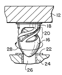
Figures 3a through 3c, show a first embodiment of the
invention. The contact element 10 is shown in Figures 3a and
3b ext~n~;ng from thé base of an integrated circuit package 12
such as a PGA. Contact element 10 generally includes a
conductive generally cylindrical portion 14 and a conductive
tapered contact portion 16. The cylindrical portion 14
generally comprises a base portion 18 and a spring portion 20
with the spring portion preferably having a plurality of
~ 94t23475 2 I S g ~ 3 PCT~S94/03393
partial helical elements. The relative sizes of the
respective base, spring and contact portion may vary according
to specific applications. Generally, however, the base
portion 18 is electrically and mechanically coupled to a
portion of a first device (in this case an ICP 12) which
requires electrical connection to a second device (e.g., a
circuit board), whereas the contact portion 16 makes
electrical connection to the second device. In Figures 3a and
3b, the second device is a PCB 24 having a hole 26 defined by
a conductive rim 22. It will be appreciated that in actual
practice, an ICP 12 will have many contact elements 10
extending from its base and PCB 24 will have many holes 26
with conductive rims 22. Those skilled in the art will
understand how electrical connection is made between the base
portion 18 of the contact element 10 and the internal circuits
of ICP 12 and how the conductive rim 22 on PCB 24 is coupled
with the circuits of the PCB. In general, however, the
coupling of the base portion 18 of the contact element 10 to
the ICP 12 is usually accomplished by soldering or brazing to
an existing conductive pad on the underside of the ICP 12.
As seen in Figures 3a and 3b, it will further be
appreciated that when the ICP 12 is pressed against the PCB
24, the spring portion 20 of contact element 10 biases the
contact portion 16 against the rim 22 of hole 26 in PCB 24
assuring a good electrical connection between the contact
portion 16 and the rim 22. According to a preferred
embodiment of the invention, as the spring portion 20 of the
contact element is biased (by applying a downward force), a
torsional rotation (shown by arrow 28 in Figure 3b) is
effected at the contact portion 16. This rotation of the
contact portion 16 causes the contact portion to rotationally
wipe the rim 22 as the contact portion extends into the hole
and axially wipes the rim, thus ensuring a good electrical
coupling. It should be understood by those skilled in the art
that any type of spring which effects a rotation during
compression can be used as the spring portion of the contact
element to effect the torsional rotation of the contact
~,s~
W094/~47~ PCT~S94/03393
16
portion. However, according to a first preferred embodiment
of the contact element, the contact portion 16, spring 20 and
base 18 are preferably manufactured as an integral piece from
a sheet of conductive material as discussed hereinafter with
reference to Figs. 3c and 3d. With the spring elements being
formed from flat stock as opposed to round, the spring
elements do not act like a classical simple coil spring.
Also, by providing a plurality of flat spring elements,
parallel electrical paths are provided, thereby reducing
inductance as opposed to a single coil spring. Further, by
designing the spring elements as desired (e.g., width,
thickness, length, twist, etc.), the parameters governing
contact forces can be controlled. Indeed, depending on the
contact environment, more or less wipe may be desired. For
example, for nobel metal systems where lots of mating cycles
may be required, less wipe may be desirable, whereas in a
non-nobel metal environment such as tin or tin-lead, where
only a few mating cycles are expected, a large wipe may be
desired and tolerated.
Turning now to Figure 3c, an exemplary embodiment is seen
of a flat blank 30 of beryllium copper used to create a
contact element 10 shown in Figures 3a and 3b. Blank 30 is
cut by a die or etched with photo-chemicals and then rolled
into a cylinder to provide the base 18, spring 20, and contact
portion 16. As shown for example in Figure 3c, the spring
portion 20 is formed by three parallelogrammatical or rhombic
holes 20b, 20c, 20d and two angular cuts 20a and 20e. It will
be appreciated that when the blank 30 is rolled into a
cylinder, cuts 20a and 20e can be connected to form a fourth
parallelogrammatical hole and thus define four helical spring
elements 20f-20i. Contact portion 16 is ~ormed by four
parabolic cuts 16a-16d which form a non-linearly tapered
contact portion when the blank is rolled into a cylinder and
the parabolic cut portions are pressed or welded together to
form the tapered contact portion. As seen in Figure 3c, the
blank 30 may be formed with other contiguous blanks, e.g. 30-1
and 30-2, from a single roll of beryllium copper flat stock
~ 3
94/~475 PCT~S94/03393
17
rolled in a progressive die to facilitate mass production of
the connector.
Turning to Fig. 3d, a second embodiment of a flat bank
30b is shown. As seen in Fig. 3d, holes 20k, 201, and 20m and
angular cuts 20j and 20n take a different form than in Fig. 3c
such that the helical spring elements 200-20r when set out
flat have a sine-wave shape. When rolled into a cylinder,
the helical spring elements 200-20r permit additional twisting
beyond what might be obtained with the arrangement of Fig. 3c.
It will be appreciated that the blanks 30 and 3Ob of
Figure 3c and 3d are but two example of how the contact
element 10 may be formed. Different numbers and shapes of
cuts and holes may be used, provided a twisting spring
arrangement results. For example, it is not necessary that
the spring portion consist of four partial helical members,
although it is believed that it is preferable to have at least
three. Moreover, the contact portion could be formed by a
different number of parabolic cuts. In fact, the contact
portion need not be formed from the flat stock, as the base,
spring, and contact portions may be formed separately and may
be connected to each other as will be described below. Also,
if desired, the contact portion may be bifurcated as taught in
the parent applications hereto or made otherwise resilient
and/or laterally tolerant. Regardless, it will be appreciated
that the twisting spring arrangement which results provides a
good wipe as it mates, and also provides excellent lateral
tolerance.
As will be appreciated, the contact element of the
invention requires an outside fastening means to keep the
spring portion biased thereby pressing the tapered contact
portion against the rim of the hole. Figure 4 shows one
example of a fastening means 40 for fastening an ICP 12 to a
PCB 24. Fastening means 40 comprises a resilient plastic post
42 having a holding lip 44 at one end, a barb 46 at the other
W094l23475 ~5~ PCT~S94/03393
18
end, and a protrusion 48 in the middle. The barb 46 is
resiliently formed so that it can be forced through hole 50 in
the circuit board 24, but cannot be easily removed once forced
through. Protrusion 48 is provided as a stop such that the
fastening means 40 can be fixed in place prior to the
placement of an integrated circuit chip 12 (shown in phantom)
onto the PCB 24. Lip 44 is provided to hold down the
integrated circuit chip 12. As indicated by the arrows and
the phantom movement of post 42, the plastic post 42 of the
fastening means 40 is flexible and resilient, and can be bent
or pushed out of the way during placement of the integrated
circuit chip 12. Once the contact portions 16 of the contact
elements lO of the integrated circuit chip 12 are resting on
top of holes 26 of the circuit board (i.e., on the rims 22 of
the holes), the chip 12 is preferably pressed down to cause
the contact portions of the contact elements lO to twist into
the rims 22, and mate therewith. The plastic post 42 is then
released into its unstressed position such that lip 44 of post
42 holds chip 12 in its mating engagement with the PCB 24.
Those skilled in the art will appreciate that preferably, at
least two fastening means 40 (one on either end of the ICP)
are provided to fasten chip 12 to board 24. In disconnecting
the chip from mating contact, the plastic posts 42 are bent
out of the way, and the chip will typically automatically back
out of mating contact and may be physically removed.
Reference is made to the parent applications cited above
which disclose other fastening means which may be used with
the connector of the present invention.
As seen in the Figures described above, the preferred
embodiment of the contact element lO includes a tapered
contact portion 16 which has a non-linear taper. In other
words, the contact portion is preferably hemispherical,
paraboloidal or the like. The reason for providing the
contact portion with a non-linear taper is to assure that
adjacent contacts will generate similar normal forces aginst
~ 2 1 5 8 2 5 3 PCT~S94/03393
19
adjacent rims, even if the adjacent rims have slightly non-
uniform diameters. In particular, it will be appreciated that
the axial force exerted on the contact portion by the spring
is translated to a normal force acting between the the contact
portion and the conductive rim of the hole. Figures 5a and 5b
show in simplified two dimensional form how the normal force
varies with a non-linearly tapered contact portion. As
exemplified in Figures 5a and 5b, the normal force vector FN
is the force perpendicular to the tangent t of the contact
portion 16 at the point where the contact portion 16 contacts
rim 22. Thus, as shown in Figure 5a, where the contact
portion 16 only enters a small part of hole 26, a tangent line
tl drawn from the point of contact between rim 22 and contact
portion 16 forms an angle e, with the vertical of 30 for
example. The normal force FN1 between the contact portion and
the rim is therefore equal to the vertical force FV~ divided by
the sine of 30 (i.e., 2FVl). In the simplified two
dimensional example of Figure 5a, and by way of example only,
if the axial force FAl exerted by spring 20 is .5 newtons, the
vertical force FV~on either side of the contact portion acting
on the rim is .25 newtons (FA~/2). The resulting normal force
FNl between the rim and the contact portion is .5 newtons on
each side for a total of 1.0 nt acting in a normal fashion
between the contact portion and the rim.
Comparatively, in Figure 5b, where the hole 26 of the
circuit board has a wider diameter, the force exerted by
spring 20 is less because the contact portion 16 extends
farther into wider diameter hole 26 and the spring is
therefore less biased. However, when the contact portion
extends deeper into the hole, the tangent line t2 drawn from
the point of contact between the contact portion and rim has
an angle e2 with the vertical of 15 for example. The normal
force between the contact portion and the rim FN2is therefore
equal to the vertical force FV2 divided by the sine of 15
(i.e., approximately 4FV2). In the simplified two ~ir?nsional
example of Figure 5b, if the axial force exerted by spring 20
is only .25 newtons because of a smaller spring compression,
~s~2~3
W094/23475 PCT~S94/03393
the vertical force FV2 on either side of the contact portion
acting on the rim is .125 newtons (FA2/2). The resulting
normal force FN2 between the rim and the contact portion is .5
newtons on each side for a total of 1.0 nt acting normally
between the contact portion and the rim. Thus, it will be
appreciated that by dimensioning the contact portion with the
proper curvature, the normal force between the rim and the
contact portion of the contact element is substantially
maintained even where the hole is wider and the contact
portion of the contact element enters deeper into the hole.
In other words, the magnification of forces due to the shape
of non-linear shape of the contact portion offsets changes in
the spring force due to more or less compression.
As mentioned above, the contact elements of the invention
can be used to connect one circuit board to another. Figure 6
shows one example of how the contact elements of the invention
can be used to mate a mother and a right angle daughter board.
In Figure 6, a section of a daughter board 52 is shown mounted
perpendicular to a mother board 24. The daughter board 52 is
provided with a connector 53 having a plurality of contact
elements, for example lOa-lOg which are arranged in any manner
consistent with accepted industry practices. In particular,
however, contact elements lOa-lOg are arranged in a pattern
which will mate with a pattern of holes 26a-26g in the mother
board 24. As with the above described embodiments, contact
elements lOa-lOg electrically couple with conductive rims
22a-22g of the holes 26a-26g on the mother board 24. In
addition, in order to align the contact elements with the
conductive rim, a guide hole 27 is preferably provided in the
mother board 24, and the connector 53 preferably is
correspondingly provided with a guide pin 54. The guide pin
54 enters guide hole 27, and if desired, the pin 54 may be
conductive and form part of the electrical connection between
the boards, and may provide a "first make" arrangement. In
this case, the guide hole 27 is advantageously provided with a
conductive lining 56 which couples to other circuitry on the
mother board in any known manner. It will be appreciated that
~ ~475 2 ~ 5 ~ 2 5 ~ PCT~S94/03393
21
several different means for fastening the mother and daughter
boards together are described in the above-referenced parent
applications.
Figures 7a and 7b show another embodiment of the
invention. As mentioned above with reference to Figs. 3a-3d,
if the contact elements are formed from flat stock, they may
be joined at cut edges to provide a substantially cylindrical
arrangement. In the embodiment of Figs. 7a and 7b, in
creating contact element 110, the stamped or etched blank is
rolled and surrounded by a cylindrical collar 11, and as seen
in Fig. 7c, not necessarily closed. Indeed, the rolled
contact element 110 may overlap (as seen in Fig. 7c), abut at
cut edges, or even fail to form a complete cylinder, provided
the base portion is adequately supported by the collar.
Regardless, the collar 11 of Figs. 7a and 7b is preferably
dimensioned so that substantially all of the spring portion 20
of the contact element is covered by the collar when the
contact element is extended to its maximum length as shown in
Figure 7a. Collar 11 and contact portion 116 of the contact
element llo are also dimensioned such that when the spring
portion 20 is compressed (i.e. when the contact portion 116
bïases a conductive rim of a hole) as shown in Figure 7b, the
contact portion 116 extends sufficiently beyond the collar 11
so that electrical contact is not impeded by the collar. It
will be appreciated that the spring portion 20 and contact
portion 116 of the contact element 110 must be free to move
axially relative to the collar, but that the base portion 18
of the contact element 110 may be mechanically fixed to the
collar 11. Alternatively, the collar may be mechanically
fixed to the device carrying the contact elements. The collar
is preferably non-conductive and may be constructed of plastic
sheet material which is cut and rolled. As will be
appreciated, a non-conductive collar serves to electrically
isolate individual contact elements from each other. As seen
in Figs. 7a and 7b, the contact portion 116 of contact element
110 is a bifurcated conical contact portion unlike the non-
linearly tapered contact portions described above. The
~58~s3
W094/~475 PCT~S94/03393
22
bifurcation provides some lateral tolerance to the system
which might otherwise be limited due to the collar of the
embodiments of Figs. 7a and 7b. It will be appreciated that
the partial helical spring concept of the invention can be
applied to any type of contact portion whether the contact
portion is tapered or not. It is, however, preferred that the
contact portion be tapered and it is further preferred that it
be non-linearly tapered as shown and described above.
Besides providing electrical insulation of the contact
element, the collar 11 shown in Figures 7a and 7b is useful as
acting as a stop for the contact element, thereby limiting the
axial compression of the spring. In fact, because the
preferred flat spring elements of the invention bend inwardly
when compressed (as shown in Fig. 7c), failure to limit the
axial compression could result in the spring elements
contacting each other. Thus, the collar not only prevents
accidental compression beyond the elastic limit of the spring,
but also prevents unwanted contact among the spring elements,
and resultingly preserves the life of the spring and contact
elements.
Figure 8a shows yet another embodiment of the invention
where a contact element 210 couples a pair of PCBs 24, 80
which are parallel to each other. The contact element 210
shown in Figure 8 is constructed of separate modular
components for the contact portion 216, the spring 20a and the
base 18a. According to the preferred modular construction of
contact element 210, the contact portion 216 and the spring
20a are fixed sizes while the base portion 18a may be made in
various sizes. This allows the base to be fashioned to any
desired length so that the overall length of the contact
element is long enough to span the distance required between
two parallel PCBs 24, 80. As shown in Figure 8a, the base 18a
of contact element 210 is surface mounted on PCB 80 in a
position which will align with hole 26 in PCB 24 when the
boards are coupled. One or more guide pins 82 are provided
2I~82~3
94/23475 PCT~S94/03393
23
for aligning the two boards in a manner similar to that
described above and in the parent applications. In addition,
one or more spacers 84 may be provided to electrically isolate
each contact element from the other contact elements. Such
spacers may also be desirable to protect components mounted on
either board from being sandwiched too tightly between the
boards; i.e., to limit the axial movement of the contact
elements 210.
Turning to Fig. 8b, a contact element 310 which is a
cross between the contact elements of Fig. 7a and 8a is seen.
The contact element 310 is preferably formed from flat stock,
punched to form spring elements 320, and rolled and formed to
form a contact portion 316 and base 318. Because the "seam"
of the base 318 is not welded or otherwise fastened together
(although it could be), an alignment jig 384 is provided which
acts both to align placement of the contact element 310 on
board 80, and to support the base portion 318 and at least
part of the spring element portion 320. In particular, as
seen in Fig. 8b, the alignment jig 384 has a stepped
configuration, with a first recessed portion 384a near PCB 80
which allows room for the soldering of the base 318 to a SMT
surface mount pad 81 as indicated by solder joints 83. The
supporting portion 384b of alignment jig 384 effectively
provides a supporting collar (as discussed above with
reference to Figs. 7a and 7b). The supporting portion 384b
supports a portion of the base 318 and a portion of the spring
portion 320 of the contact element, such that the contact
element 310 need not be fastened to form a cylinder. As
shown, the supporting portion 384b does not extend all of the
way up to the contact portion 316 of the contact element 310.
Rather, a second recessed portion 384c is provided which acts
to provide a stop while still providing the contact element
310 adequate lateral flexibility (shown in phantom at the tip
of the contact element) as it mates with the conductive rim 22
of PCB 24 similar to the embodiment of the contact element of
Fig. 8a.
W094/23475 ~5~ PCT~S94/03393
24
Turning to Figure 9, another modular contact element 410
similar to contact element 210 of Fig. 8a is seen, but the
contact element 410 is constructed of five sections: contact
portion 216; first spring 20a; bridge 21; second spring 20b;
and base 18b. In this embodiment, it should be noted that the
springs 2Oa, 2Ob are mounted with their turns opposite each
other so that the compression of the contact element 410
effects only a limited rotation of the contact portion 216.
The length, element thickness, helicicity, etc. of the spring
2Ob may be chosen as desired to control the parameters of the
contact element 410 such as the torque, axial spring rate,
etc. Thus, by adding the additional spring 2Ob, the contact
element 410 is provided with an additional degree of freedom.
For example, a desired amount of the rotation generated by the
helical springs 20a may be absorbed by the oppositely wound
springs 20b. Such an arrangement might be useful when the
contact elements of the invention are used to couple with
conductive rims made of a soft metal such as gold and repeated
connection and disconnection is anticipated, as a very strong
wiping rotation of the contact portion might tend to wear
excessively against the soft metal rim. It is noted that the
contact element 310 may be stamped or etched from flat stock
as described with reference to Figs. 3c and 3d, or otherwise
formed as desired.
It will be appreciated that many variations to the
contact element 410 of Fig. 9 may be provided. Rather than
having the spring arranged with turns opposite each other, it
may be desirable to have the turns arranged in the same
direction. Such an arrangement might provide yet additional
torque to the system without compromising the integrity of the
spring elements. Further, it will be appreciated that more
than two spring portions could be arranged in tandem as
desired.
21582.~`
94/~475 PCT~S94/03393
There have been described and illustrated herein several
embodiments of a spring biased contact elements which provide
rotational wipe (torque) when mating and are useful in
electrical connectors and in conjunction with integrated
circuits. While particular embodiments of the invention have
been described, it is not intended that the invention be
limited thereto, as it is intended that the invention be as
broad in scope as the art will allow and that the
specification be read likewise. Thus, while particular
partially helical springs have been disclosed, it will be
appreciated that other kinds of springs could be utilized.
Also, while certain tapered contact portions have been shown,
it will be recognized that other types of contact portions
such as disclosed in the parent applications hereto could be
used with similar results obtained. Moreover, while
particular materials and dimensions have been disclosed, it
will be appreciated that other materials and dimensions could
be used as well. In addition, while it is generally preferred
that the contact elements be entirely conductive, it may be
advantageous to make part of the contact element non-
conductive. For example, while the conductive contact portion
must be electrically coupled to the device carrying the
contact element, the spring portion could be non-conductive
provided that the contact portion is electrically coupled to
the carrying member by a flexible wire or the like. Further,
it will be appreciated that aspects of the the described
embodiments can be mixed and matched with other aspects of
other described embodiments. It will therefore be appreciated
by those skilled in the art that yet other modifications could
be made to the provided invention without deviating from its
spirit and scope as so claimed.