Note: Descriptions are shown in the official language in which they were submitted.
2158394
APPARATUS FOR READING FROM AND/OR WRITING ONTO DATA
CARRIER CARDS HAVING AT LEAST ONE OPTICAL MEMORY AREA
AND ONE CHIP MEMORY AREA
Because of the technical development in recent years, optical memory cards in
5 credit card format which can be written onto and read from by means of laser
beams ("WORM" = write once read many) have achieved storage ~apacities of
several megabytes, in particular 4 to 6 megabytes. Reading/writing devices
have developed correspondingly. In contrast to magnetic storage on floppy
disks, the optically stored data are insensitive to mechanical and
10 electromechanical influences. They are thus suitable for being carried on one's
person, for example in wallets.
Chip cards in credit card format contain one or more electronic memory and/or
processor chips which are put into the card, there being arranged on the
surface of the card sheet-like metallic contacts, onto which correspondingly
15 arranged contact pins of the read/write head are pressed. Chip cards are usedin particular as credit cards (debit cards) for the payment of telephone calls,
entry tickets or parking charges. Designed as processor cards, they may have
a read-only memory (ROM) with 1 to 10 kilobytes of storage capacity for the
operating or user software and up to 2 megabytes of storage capacity as main
20 memory. In particular cards equipped with a processor chip open up diverse
possibilities in the area of electronic encoding (cryptography).
It has also already been proposed to equip memory cards both with an optical
memory area and with a chip memory area (so-called hybrid cards), see for
example U.S. Patent 5,185,798.
Le A 30 661-US/FC
- 2158~94
Use of the hybrid card requires separate reading/writing devices for the opticalmemory area on the one hand and the chip memory area on the other hand,
since the two memory areas require fundamentally different reading/writing
techniques. In the case of the optical card, the optical memory area is scanned
5 by a laser read/write head in two dimensions, the card generally being moved
on a card carrier back and forth in one dimension (line scanning) and the
read/write head being moved back and forth over the card in another dimension
(column scanning). The reading from and writing onto the chip on the other
hand is performed by means.of normally closed contacts.
10 In the interests of effective use of hybrid cards, it would be desirable to have
both the optical memory area and the chip memory area accessible
simultaneously. For example, for many applications it is expedient to store the
directory (index) for the data stored in the optical memory area, of comparably
low access speed, in the chip memory area, which can be accessed quickly. In
15 particular, when writing onto the optical memory area, access to the chip foridentifying a free memory location and, after writing, storage of the new
memory address in the chip would be possible without moving the card from
one reading device into the other.
Furthermore, the cryptographic possibilities of a hybrid card are considerably
20 extended by the encoding and decoding processor of the chip being
simultaneously available during reading from and writing onto the optical
memory area.
The object of the present invention is to provide a reading/writing device whichallows the data of both memory areas of a hybrid card to be accessed
25 simultaneously and the memory areas to be written onto simultaneously.
The subject of the present invention is an apparatus for reading from and/or
writing onto data carrier cards having at least one optical memory area and at
Le A 30 661-US/FC - 2 -
- ~158394
least one chip memory area, the apparatus including a card carrier for receivingand fixing the data carrier card, the card carrier being movable back and forth
in a first direction in the card carrier plane over a length which corresponds at
least to the longitudinal dimension of the optical memory area of the card, an
5 optical read/write head, which is movable back and forth in a second directionabove the card plane and parallel with respect to the latter over a length whichcovers at least the width of the optical memory area of the card, the bearing
surface of the card carrier for the card furthermore having a recess into which
the chip contact is put.
10 The invention is explained in more detail below with reference to the drawings,
wherein:
Fig. 1 shows the front side and rear side of a hybrid card which can be used
according to the invention.
Fig. 2 shows an alternative rear side of the card which can be used according
to the invention.
Fig. 3 shows the reading/writing device according to the invention.
Fig. 4 shows a data processing environment of the reading/writing device
according to the invention.
Referring now more particularly to the drawings, Fig. 1 shows the front side A
20 with the optical memory area 1 of a hybrid card which can be used according
to the invention. The rear side B of the card contains the chip, which has, by
way of example, six contacts within the contact surface 2.
Le A 30 661-US/FC - 3 -
- ~15839~
Fig. 2 shows the rear side B of an alternative hybrid card, which has a
multiplicity of additional chips 3, which can be driven via a common contact
surface 2.
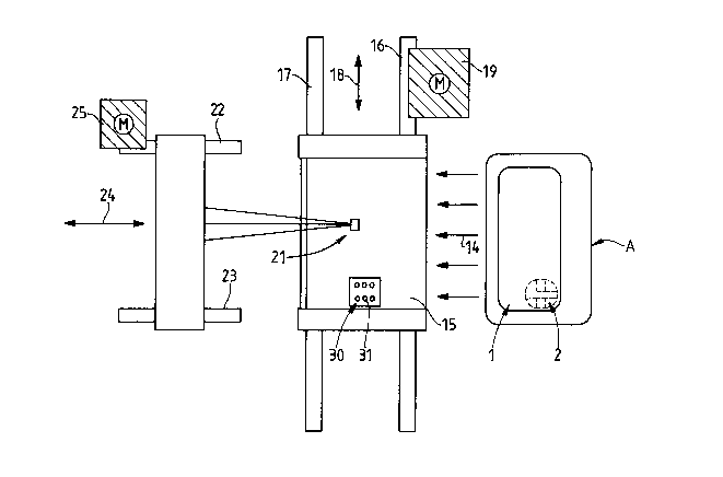
Fig. 3 shows the hybrid card A with the optical memory area 1 facing upwards,
5 with the contact surface 2 for the chip Iying underneath the card. The
reading/writing device has a card carrier 15, in which the card is pushed in thedirection of the arrows 14. The card carrier 15 is movable back and forth in thedirection of the double-headed arrow 18 on slide rails 16, 17 with the aid of a
drive mechanism 19. The optical read/write head 21 is movable back and forth
in the direction of the double-headed arrow 24 on the slide rails 22, 23 with the
aid of the drive mechanism 25, so that the combined movement along the
double-headed arrows 18 and 24 allows the scanning of the optical memory
area 2 of the memory card A pushed into the carrier 15. To this extent these
are commercially available reading/writing devices for optical memory cards,
15 such as are commercially available under the designations Conlux LC-304,
Olympus CS 2000 or Canon RW-20.
According to the invention, a contact 30 with contact pins 31 is put into the
card table 15, into the card carrier 15, in such a way that, after the pushing in
of the hybrid card A into the card table 15, the contact pins 31 come into line
20 with the corresponding regions of the contact surface 2. Signal transmission
from contact 30 to the downstream data processing devices can take place via
a freely movable ribbon cable.
Fig. 4 shows the front side A and the rear side B of a hybrid card in a data
processing environment, for example a PC environment.
25 It will be understood that the specification and examples are illustrative but not
limitative of the present invention and that other embodiments within the spiritand scope of the invention will suggest themselves to those skilled in the art.
Le A 30 661-US/FC - 4 -