Une partie des informations de ce site Web a été fournie par des sources externes. Le gouvernement du Canada n'assume aucune responsabilité concernant la précision, l'actualité ou la fiabilité des informations fournies par les sources externes. Les utilisateurs qui désirent employer cette information devraient consulter directement la source des informations. Le contenu fourni par les sources externes n'est pas assujetti aux exigences sur les langues officielles, la protection des renseignements personnels et l'accessibilité.
L'apparition de différences dans le texte et l'image des Revendications et de l'Abrégé dépend du moment auquel le document est publié. Les textes des Revendications et de l'Abrégé sont affichés :
| (12) Demande de brevet: | (11) CA 2158394 |
|---|---|
| (54) Titre français: | APPAREIL D'ENREGISTREMENT ET DE LECTURE POUR CARTES DE STOCKAGE DE DONNEES COMPORTANT AU MOINS UNE MEMOIRE OPTIQUE ET UNE PUCE-MEMOIRE |
| (54) Titre anglais: | APPARATUS FOR READING FROM AND/OR WRITING ONTO DATA CARRIER CARDS HAVING AT LEAST ONE OPTICAL MEMORY AREA AND ONE CHIP MEMORY AREA |
| Statut: | Réputée abandonnée et au-delà du délai pour le rétablissement - en attente de la réponse à l’avis de communication rejetée |
| (51) Classification internationale des brevets (CIB): |
|
|---|---|
| (72) Inventeurs : |
|
| (73) Titulaires : |
|
| (71) Demandeurs : |
|
| (74) Agent: | SMART & BIGGAR LP |
| (74) Co-agent: | |
| (45) Délivré: | |
| (22) Date de dépôt: | 1995-09-15 |
| (41) Mise à la disponibilité du public: | 1996-03-20 |
| Licence disponible: | S.O. |
| Cédé au domaine public: | S.O. |
| (25) Langue des documents déposés: | Anglais |
| Traité de coopération en matière de brevets (PCT): | Non |
|---|
| (30) Données de priorité de la demande: | ||||||
|---|---|---|---|---|---|---|
|
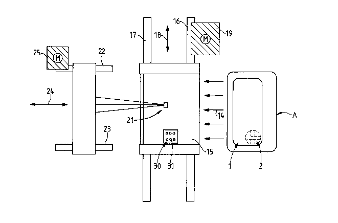
An apparatus for reading from and/or writing onto data carrier cards
having at least one optical memory area and at least one chip memory area,
the apparatus having a card carrier for receiving and fixing the data carrier card
and an optical read/write head, the card carrier and read/write head being
movable back and forth in different directions in planes parallel with respect to
the bearing surface of the card carrier for the card, and there being provided in
the bearing surface of the card carrier for the card a recess into which the chip
contact is put.
Note : Les revendications sont présentées dans la langue officielle dans laquelle elles ont été soumises.
Note : Les descriptions sont présentées dans la langue officielle dans laquelle elles ont été soumises.
2024-08-01 : Dans le cadre de la transition vers les Brevets de nouvelle génération (BNG), la base de données sur les brevets canadiens (BDBC) contient désormais un Historique d'événement plus détaillé, qui reproduit le Journal des événements de notre nouvelle solution interne.
Veuillez noter que les événements débutant par « Inactive : » se réfèrent à des événements qui ne sont plus utilisés dans notre nouvelle solution interne.
Pour une meilleure compréhension de l'état de la demande ou brevet qui figure sur cette page, la rubrique Mise en garde , et les descriptions de Brevet , Historique d'événement , Taxes périodiques et Historique des paiements devraient être consultées.
| Description | Date |
|---|---|
| Inactive : CIB de MCD | 2006-03-11 |
| Inactive : CIB de MCD | 2006-03-11 |
| Le délai pour l'annulation est expiré | 1998-09-15 |
| Demande non rétablie avant l'échéance | 1998-09-15 |
| Réputée abandonnée - omission de répondre à un avis sur les taxes pour le maintien en état | 1997-09-15 |
| Demande publiée (accessible au public) | 1996-03-20 |
| Date d'abandonnement | Raison | Date de rétablissement |
|---|---|---|
| 1997-09-15 |
Les titulaires actuels et antérieures au dossier sont affichés en ordre alphabétique.
| Titulaires actuels au dossier |
|---|
| BAYER AKTIENGESELLSCHAFT |
| Titulaires antérieures au dossier |
|---|
| GEORG HARTMANN |
| GUNNAR WEIKERT |
| HANS-GERD WETTLAUFER |
| JOACHIM ARTZ |

