Note: Descriptions are shown in the official language in which they were submitted.
~O 94/22236
PCT/US94/02025
- 1 -
METHOD AND APPARATUS FOR SIGNAL TRANSMISSION AND RECEPTION
FIELD OF THE INVENTION
This invention relates to signal transmitting and
receiving systems and more particularly to signal
decomposition and reconstruction techniques in signal
transmission and reception systems.
$ACKGROUND OF THE INVENTION
As is known in the art, a modulator-demodulator (modem)
is an electronic device that modulates transmitted signals
and demodulates received signals. The modem generally
provides an interface between an analog communications system
and digital devices to thus make possible analog transmission
of digital information between two terminals or stations.
Such transmissions may be over a transmission line, such as
a telephone or other communication line for example, coupled .
between the two stations. Such transmission lines are
generally band-limited. That is, the information may be
transmitted over the transmission lines only over a
predetermined range of frequencies. For example, telephone
transmission lines are generally provided having a bandwidth
of 3 kilohertz (kHz). Thus, the speed with which the modem
may transmit and receive data is limited, in part, due to
bandwidth limitations of the transmission medium.
As is also known, an analog signal representing, e.g.
a voice signal, may be represented as a stream of bits (i.e
a digital signal). The digitized signal, which may be
converted back to an analog representation of the digital
data for the purpose of transmission over a telephone lines,
is less susceptible to noise on the telephone line, is
capable of multiplexed channel operation in the telephone
bandwidth, reduces crosstalk and enables relatively easy
digital encryption for secure transmission.
The digitized voice signal, which typically is at, e. g. ,
64,000 bits-per-second (bps), may not be readily sent by
WO 94/22236 PCT/US94/02025
- 2 -
modem within the available approximately 3,000 Hz bandwidth
of the telephone lines or be readily sent at that bit rate
within the available telephone line bandwidth. To enable more
convenient transmission and/or multiplexed transmission,
v
compression of the 64,000 bps digitized voice signal is
generally employed. For example, with compression from
64,000 bps to 2,400 bps, four simultaneous channels of 2,400
bps each may be multiplexed via a modem onto a 9, 600 bps data
stream transmitted over the bandwidth of the analog telephone
lines.
As is also known in the art, encryption of analog
signals such as voice signals, for example, may be
accomplished via analog or digital techniques. Analog
techniques include frequency inversion and other operations
(e. g. modulation) on the amplitude, frequency or phase of the
time varying analog signal. Such operations may or may not
be accomplished with a digital computer.
Digital voice encryption techniques, including the
American National Standard Institute's (ANSI) data encryption
standard (DES) algorithm, perform bit stream operations on
digitized samples of the analog signal and then transmit the
digital result to a receiver. Such transmission may be
accomplished through a modem for example. To use a modem for
transmission of a speech signal, the speech signal is
compressed. That is, some of the input information (i.e. the
input speech signal) is discarded such that the signal may
be transmitted at a rate at which the modem operates. This
results in a loss of information which may manifest itself
as a degradation in voice sound quality.
The processing required to perform the compression and
expansion of digitized voice results in an undesirable delay
and consequently in a two line transmission system, for
example, objectionable echo signals.result. Furthermore, the
inefficiency of modems limits the rate at which a modem may
transmit and receive signals fed thereto. Thus it would be
desirable to provide a system which minimizes such processing
~O 94/22236
PCT/US94/02025
- 3 -
time and thus minimizes the echo signal and also maximizes
the rate at which a modem may transmit and receive data over
a transmission link.
Thus, at least several problems have tended to impair
the effectiveness of conventional limited bandwidth, e.g.,
telephone bandwidth, analog and digital voice transmission
apparatus.
SUMMARY OF THE INVENTION
In accordance with the present invention a modem
includes a modulator, for receiving on each of a plurality
of modulator channels an input sample, wherein the modulator
groups the first plurality of input samples to form an input
data frame and wherein the modulator multiplies the input
data frame by a first rotation matrix having a row dimension
and a column dimension corresponding to the number of
channels in the modulator to provide an output data frame
corresponding to a modulated output signal. The modem
further includes a demodulator, having a plurality of
channels, for receiving a data frame corresponding to a
modulated output signal provided from a first plurality of
input samples, wherein the demodulator multiplies the
received data frame by a second rotation matrix having a row
dimension and a column dimension corresponding to the number
of channels in the demodulator to provide a de-modulated
signal corresponding to an output data frame having a first
plurality of output samples, wherein the demodulator provides
on each of the demodulator channels a corresponding one of
the first plurality of output samples wherein each of the
output samples correspond to one of the first plurality of
input samples. With this particular arrangement, a modem
based on an invertible transform which operates on groups of
input samples is provided. The invertible transform is here
provided' by application of the rotation matrix. ~ By
multiplying each of the data frames in the modulator by the
first rotation matrix a signal may be transmitted over a
transmission link at a relatively high data rate. The
21 ~ 8:~~4t~,~ . t
WO 94/22236 PCT/US94/02025
- 4 -
modulated data frame may then be sent over a transmission
link and received in a demodulator of a second modem. The
demodulator demodulates the received modulated data frame by
multiplying the received modulated data frame by a second
rotation matrix which performs the inverse operation of the
first rotation matrix and thus provides a demodulated signal.
The demodulated signal may then be fed to a receiver for
further processing. The transform provided by the rotation
matrix is computationally simple and thus results in a lower
delay time than conventional techniques. A coding circuit
may be coupled to at least one channel of the modulator to
provided a coded modulated data frame. A corresponding
decoding circuit may be coupled to a corresponding channel
of the demodulator of the second modem to thus decode the
coded modulated data frame. A timing circuit coupled between
the first and second modems provides timing signals to each
of the first and second modems.
In accordance with a further aspect of the present
invention, a method and apparatus for providing a modem for
sending digital data over an analog medium includes a
synthesizer to provide a modulator and an analyzer to provide
a demodulator. With this particular arrangement, digital
data to be transmitted may be applied to the input ports of
the synthesizer. In a preferred embodiment the data may be
scrambled by a random number generator coupled to the
synthesizer to thus provide an encrypting modem. Such a
modem may be provided using relatively simple hardware and
thus the modem may be provided as a portable encrypting
modem. The modulation and demodulation operations may be
accomplished using invertible transform techniques which
result in faster processing operations and thus result in a
shorter delay. Thus, the modem may transmit and receive
l
signals at a higher data rate than
modems heretofore.
In accordance with a still further aspect of the present
invention a signal encryptor includes an analyzer, for
decomposing an input signal into a plurality of analyzer
94/22236 ~ .~e, PCT/US94I02025
- 5 -
signals, each of said analyzer signals provided on one of a
plurality of analyzer channels and an encryptor circuit,
coupled to each of the analyzer channels, for modifying at
0
least one of the analyzer signals. The signal encryptor
further includes a synthesizer, having a plurality of
synthesizer channels each of the synthesizer channels coupled
to a corresponding one of the analyzer channels, wherein the
synthesizer receives each of the plurality of analyzer
signals fed thereto and combines the plurality of analyzer
signals into a reconstructed output signal corresponding to
an encrypted input signal. With this particular arrangement,
a signal encryptor for encrypting sampled signals for secure
transmission over a transmission medium or link without
compression is provided. The signal encryptor and likewise
a corresponding signal decryptor may be provided from an
inverse transform such as a rotation matrix. The rotation
matrix operates on a block of encrypted data signals to
provide an encrypted data frame for transmission over the
transmission link. The signal encryptor may further be
provided having an input signal conditioning circuit coupled
to the analyzer input for appropriately filtering and
sampling, with an analog to digital converter, an analog
signal fed thereto. The signal encryptor may further be
provided having an output signal conditioning circuit coupled
to the synthesizer output for appropriately converting
sampled a digital signal fed thereto to an analog signal and
for coupling the analog signal to an signal encryptor output
port through a filter having appropriately selected filter
characteristics. The signal en~ryptor operates such that the
spectrum of the input signal may be modified at each
frequency, or band of frequencies, by a secret number. The
transmitted signal approximates white noise and thus the new
- spectrum conceals the original signal. A receiver inverts
the operation.
_ The method and apparatus of the present invention thus
provides an invertible transform technique for modifying the
WO 94/22236 ~ PCT/US94/02025
i. d ,
1_: v.
- 6 -
spectrum of the transmitted signal at each frequency or band
of frequencies by a value which may be for example a secret
number. The modified spectrum conceals the original signal
fed from a transmitter to a transmission link. Upon
reception, a receiver inverts the transform operation to
exactly recover the original signal. Thus, by providing an
analyzer for separating an incoming signal into a plurality
of signals using an invertible transform and a synthesizer
fed by each one of the plurality of signals for
reconstructing the plurality of signals using an inverse
transform, the original input signal may be recovered at the
synthesizer output port.
BRIEF DESCRIPTION OF THE DRAWINGS
The foregoing features of this invention as well as the
15' invention itself may be more fully understood from the
following
detailed description of the drawings in which:
FIG. 1 is a diagrammatical representation of a signal
decomposition-recomposition system;
FIG. 1A is a diagrammatical representation of a cascade
analyzer;
FIG. 1B is a diagrammatical representation of a cascade
synthesizer;
FIG. 1C is a diagrammatical representation of a tree
analyzer;
FIG. 1D is a diagrammatical representation of a tree
synthesizer;
FIG. 2 is a block diagram of a signal encryptor;
FIG. 3 is a block diagram of a transmitting and
receiving system for the transmission and reception of secure
signals;
FIG. 4 is a block diagram of a signal encrypting
transmitting and receiving system;
. FIG. 5 is a block diagram of a modem;
FIG. 6 is a block diagram of a coded modem;
~O 94/22236 ~ PCT/LTS94/02025
FIG. 7 is a block diagram of a coded tree modem;
FIG. 8 is a block diagram of a system for receiving and
transmitting compressed signals;
FIG. 9 is a block diagram of a signal compression system
for transmitting and receiving signals over a digital link;
and
FIG. 10 is a block diagram of a modem.
DESCRIPTION OF THE PREFERRED EMBODIMENTS
Referring now to Fig. 1 a signal decomposition-
l0 recomposition system 10 includes an analyzer 12 having an
input port 14a and a pair of output ports 16a, 16b. Each of
the output ports 16a, 16b are coupled to a corresponding pair
of input ports 18a, 18b of a synthesizer 20.
An analog input signal X fed to the analyzer input port
14a is decomposed into a pair of signals W' and V' each of
which is fed to a corresponding one of the output ports 16a,
16b. Similarly, a pair of input signals W'
V' fed to the
,
synthesizer input ports 18a, 18b are reconstructed in to an
output signal Y at a synthesizer output port 22a. The
decomposition and reconstruction processes performed by the
analyzer 12 and the synthesizer 20 as well as the signals V'
and W' will be described further hereinbelow. Suffice it
here to say that the input signal X is decomposed into the
signals V' and W' such that the signals V' and W' may later
be combined to exactly reconstruct the input signal X.
It should be noted that the sub-analyzer and sub-
synthesizer building blocks operate digitally, however, for
clarity in the description, the signal conditioning circuits
required to convert between analog signals and digital
signals in the system have been omitted. Such signal
conditioning circuits will be described in conjunction with
FIG. 4 below. Briefly, however, and as will be described in
conjunction with Fig. 4, when an input signal to a system
building block, e.g. a sub-analyzer or sub-synthesizer,
corresponds to an analog signal, the signal should first be
4
WO 94/22236 : PCT/LTS94/02025
2~~8440
_8_
fed through a filter having filter characteristics selected
to provide Nyquist filtering. The appropriately filtered
signal may then be sampled by an analog-to-digital converter
(ADC) . Similarly, if the output from a system building block
is to be an analog signal, the signal should be fed to a
digital-to-analog converter (DAC) and fed to a second filter
likewise selected having filter characteristics selected to
provide Nyquist filtering.
The sub-synthesizer 20 performs the inverse operation
of the sub-analyzer 12, and vice versa. That is, if the
signals W~ and V' from a sub-analyzer are applied as input
signals to the sub-synthesizer input ports 18a, 18b, the
output signal Y will be identical to the sequence of input
samples, X, except for a predetermined time delay. In a
preferred embodiment, the time delay corresponds to one
sample time.
Likewise, applying the signals V~, W~ to the respective
synthesizer input ports 18a, 18b and then applying the
resultant output signal Y to the analyzer input port 14a
should provide at the respective analyzer output ports 16a,
16b the original input signals V~ and W~.
As described above, the analyzer 12 and synthesizer 20
provide signal decomposition and reconstruction functions.
As will be described below, the sub-analyzer and sub-
synthesizer may be used as building blocks and may be coupled
to provide more complex circuits which may themselves be
coupled to provide a variety of signal transmitting and
receiving systems. Furthermore, the analyzer 12 and
synthesizer 20 as well as other system building blocks to be
3o described hereinbelow may be efficiently implemented in
hardware, software or by a combination of hardware and
software.
The analyzers and synthesizers to be described herein
operate on an ordered sequence of numbers, which may be, but
are, not limited to, samples from an analog to digital
converter (ADC). For example, samples may be expressed as
~O 94/22236 ~ ~ PCT/US94/02025
;, .' , ~ ~ r
- g
X(0), X(1), X(2), and X(3) where X(0) is the most recent
sample. Each of the binary numbers X(0) through X(3) has a
particular value within a predetermined range of values. An
8-bit ADC, for example, may provide a range of decimal values
between -128 to +127.
The sequence of samples X(0) through X(3) may be
considered as the coordinates of a vector [X) in a 4-
dimensional space. A linear transformation may be made from
the coordinate system of X to another coordinate system in
the same 4-dimensional space. Thus, the vector X may be
transformed to a vector Y by a "rotation" matrix C. In
matrix notation this may be expressed as:
[Y~=[~l*[Xl
Using axes of the new coordinate system that are
mutually orthogonal, the vector Y has components which
correspond to the projections of X onto the new
transformation axes. Such projections are provided by
forming a vector dot product.
In a 4 dimension case for example, a set of Walsh codes,
Code 1 - Code 4, may be provided as:
Code 1 = +1 +1 +1 +1
Code 2 = +1 -1 +1 -1
Code 3 = +1 +1 -1 -1
Code 4 = +1 -1 -1 +1
The Walsh codes Code 1 - Code 4 above represent an orthogonal
coordinate axis in the 4-dimensions of this time ordered
space. Codes 1 - 4 have a length corresponding to the square
root of 4, (i.e. the dot product of code 1 with itself equals
4) and thus are not unit vectors.
The rotation matrix C may be expressed as:
C1 - +1 +1 +1 +1
[C) - ~ C2 - +1 -1 +1 -1
C3 - +1 +1 -1 -1 ,
C~ - +1 -1 -1 +1
That is, the rows CI - C4 of the rotation matrix C
correspond to the components of the Walsh code vectors such
WO 94/22236 PCT/US94/02025
~~.~~44~
- 10 -
that matrix multiplication between the rotation matrix C and
the vector X is equivalent to the dot product of a particular .
one of the vectors C1 - C4 with the vector X. The components
of the row vector X may be expressed as:
[x] - [x(o) , x(1) , x(2) , x(3) ]
A new state vector Y may be expressed as:
[Y] - [ [C1] * [x] , [C2] * [x] , [C3] * [x] , [C4] * [x] ]
where * symbolizes a dot product operation between [X], and
the Walsh vectors [ C1 ] through [ C4 ] . The new state vector [ Y ]
completely describes the original state defined by [X] and
may be computed on every group of 4 samples X(0) - X(3).
The linear rotation operation is exactly invertible, and
thus:
[x7 - [~~][Y]
where [C~] is the inverse of [C]. The matrix C~ may be found
from the relation:
[c~] - 1/L [c]
where L corresponds to the dimension of a row or column
vector of the matrix C~.
In a two dimensional case, Walsh vectors may be
expressed as CI = [+1,+1] and C2 = [+1,-1]. Thus, analyzers
may be defined having 2 outputs using the 2-dimensional
vector above.
Walsh vectors of any dimension may be generated by the
two dimensional vectors CI, CZ. That is, substitution of a
set of Walsh codes into a 2-dimensional generator matrix
provides a new Walsh code having twice the dimension. Using
this procedure an N-dimensional transformation needed to
provide an analyzer, may be provided. Thus, because of the
way that Walsh vectors are constructed from their two
dimensional Walsh generators, higher dimension analyzers and
synthesizers may be constructed from the 2-dimensional case.
With this matrix transformation method, matrix equations
f or . providing a modem or a s igna 1 encryptor may be generated .
94/22236 ~ ~ PCT/US94102025
- 1l -
The fundamental operation in the requisite computations is
addition and subtraction of terms.
It should be noted that in the case of a cascade
analyzer or synthesizer provided using the matrix method with
a matrix having N dimensions, the lowest frequency channel
is operated on by the matrix vector C1 and each subsequent
channel i is operated on by a corresponding matrix vector C;
until the highest frequency channel is operated on by the
matrix vector CN. Thus, in the case of a 4 dimension matrix
the lowest frequency channel is operated on by the matrix
vector C1 and the highest frequency channel is operated on by
the matrix vector C4. The case of a tree analyzer or
synthesizer provided by the matrix method will be described
in conjunction with FIGs. 1C and 1D below.
In another preferred method the equations which describe
the sub-analyzer output signals V' and W' may be provided as:
V' = SHIFT*X(n-1) - BN*W' Equation 1
W' = 2*X(n-1) - X(n) - X(n-2) Equation 2
In which:
V' corresponds to a scaling or filtering function of the
sampled input signal X;
W' corresponds to a residual or derivative of the
sampled input signal X;
X(n) corresponds to the most recent input sample;
X(n-1) and X(n-2) correspond to the two previous input
samples;
SHIFT corresponds to a variable set equal to a positive
power of 2 (such as 32, or 64, or ...); and
BN corresponds to a positive integer having a value
between 0 and SHIFT and is preferred to have a relatively
small value.
As will be explained further below the scaling function
V' and the residual W' defined by Equations 1 and 2 may be
evaluated on alternate input samples of the input signal X,
such that the value of the residual W' corresponds to twice
the difference between the "center" sample, X(n-1), and the
WO 94/22236 PCT/US94/02025
- 12 -
midpoint of a line connecting the two nearest neighbors of
X(n-1) here, the two nearest neighbors being represented as
X (n) and X (n-2 ) . When Equations 1 and 2 are evaluated on
alternate input samples, only the odd numbered (or
alternatively only the even numbered) center points are
selected for the calculation. Thus, the output rate of the
sub-analyzer corresponds to one-half the input rate of the
input signal X.
The residual W' may also be interpreted as a
deceleration about the center point. Thus it is possible to
define the residual W' as an acceleration and substitute -W'
for W' in the Equations 1 and 2 above to provide an
alternate and essentially equivalent expression for the
residual W'.
Other implementations using more nearest neighbor points
and which define the residual W' as a higher order or first
order derivative of the function evaluated about the center
point, may also be used.
The interpretation of the residual W'(N) described above
indicates that the residual W'(N) responds only to changes
in the slope around alternate samples. Thus one
characteristic of the residual W' in the present invention
is that the residual W' is provided having a value of zero
when the slope about the center point is constant.
. The conventionally defined residual W(n) is related to
the effective residual W'(n) as defined in the present
invention by
W (n) _ B * W. (n)
As a consequence of the definition for the residual
W'(n) in the present invention, signal compression based on
linear or non-linear quantization of the residual W'(n)
(rather than the residual W(n) as defined in the conventional
approach)' may result in improved performance over compression
schemes based upon conventional definitions of the residual
W(N),such as:
W(N) - X(n-1) - V(N)
O 94/22236
PCTIUS94/02025
- 13 -
The sub-synthesizer operation may be described by
equations 3 and 4 below:
Y(n-1) - Y'(n-1)/SHIFT Equation 3
Y(n) - Y'(n)/SHIFT Equation 4
in which:
SHIFT corresponds to a power of 2 and
Y'(n-1) - V' + BN*W';
Y'(n) - 2*Y'(1) - Y'(-) -SHIFT*W'; and
Y'(-) corresponds to a saved, previously calculated
(i.e. recursive), value of Y'(n).
By defining the variable SHIFT, as above and taking
advantage of the fact that multiplication and division by a
power of two is equivalent to a right or left shift on a
binary computer, practical implementations of these equations
may be provided with relatively little and simple hardware
and are therefore preferred.
Thus in the approach of the present invention, the
residual W' has been defined to provide a particular
characteristic and the sequence V' is selected to provide the
remainder of the sequence.
Referring now to FIG. 1A, a so-called "cascade analyzer"
24 includes a plurality of here N sub-analyzers. The cascade
analyzer 24 may be provided by feeding the signal V' 1 from an
output port of a first sub-analyzer 24a into the input port
. of a second sub-analyzer 24b and feeding a signal V'2 from
the output port of the second sub-analyzer into the input
port of a third analyzer (not shown) and so on. The process
continuing until a sub-analyzer 24N provides a signal V'N
having a predetermined sample rate.
For example, in a communication system it may be
desirable to couple a plurality of say N sub-analyzers as
described above where N is selected such that a signal V'N is
selected such that the signal V'N is provided having a sample
rate which is below twice the lower frequency cutoff of the
communications link. Since each sub-analyzer halves the
sample rate to its input, the various output signals, W'1,
WO 94/22236 PCT/US94/02025
- 14 -
W'Z...W'N of the cascade analyzer are provided at differing
rates.
Referring now to FIG. 1B a so-called "cascade
synthesizer" 26 may be provided from a plurality of sub-
synthesizer 26a - 26N which may be of the type described
above in conjunction with FIG. 1. The cascade synthesizer
operates to provide the inverse operation of the cascade
analyzer.
Referring now to FIG. 1C a so-called "tree analyzer" 28
may be provided by appropriately coupling a plurality of sub-
analyzers 29a - 29g each of which may be of the type
described above in conjunction with FIG. 1. Thus, in
addition to a cascade emanating from the scale function
V(N), it is also possible to have residual cascades
emanating from one or more residual sequences W'(N). That
is, the residual sequences W' (N) may themselves be considered
as inputs for a multiresolution analysis. It is therefore,
in that case, possible to provide both the scaling function
sequence V' and the residual sequence W' having equal same
sample rates. Here, the sample rate corresponding to one-
eighth the original sample rate.
The tree analyzer 28 may be provided by analyzing each
of the residual sequence outputs W until all such sequences
are brought down to one rate, which is normally below the
Nyquist rate of the lower cutoff frequency of a transmission
link with which the analyzer cooperates. The three level
analyzer tree 28 is here provided having all of its output
29a - 29h at 1/8 the sample rate, r, of the analog input
signal, X. Each output sample may include many more bits per
sample than the input sample, however, the numbers
represented by those output samples will usually be small in '
magnitude and easily requantized by a quantizer (not shown).
Referring now to FIG. 1D a so-called "tree synthesizer"
30 may be provided from a plurality of sub-synthesizers 31a
- 31g, each of which may be of the type described above in
94/22236 PCT/LTS94/02025
r
- 15 -
conjunction with FIG. 1. The tree synthesizer 30 provides
the inverse operation of the tree analyzer 28 (FIG. 1C).
It should be noted that in each of the applications to
be described herein below in conjunction with FIGS. 2-8, the
term analyzer as used throughout FIGs. 2-8 may be used to
indicate a sub-analyzer, a cascade analyzer, or a tree
analyzer element and likewise, the term synthesizer referred
to in FIGS. 2-8 may be used to indicate a sub-synthesizer,
a cascade synthesizer or a tree synthesizer element, each of
which have been described above in conjunction with FIGS. 1
1D. Each of the analyzer and synthesizer elements may be
provided according to the matrix transformation technique or
alternatively each of the analyzer and synthesizer elements
may be provided according to the three point equations of the
forms of Equations 1 and 2 above, or alternatively still,
each of the analyzer and synthesizer elements may be provided
according to equations of the form:
W' = X(n) - X(n-2)
V' = X(n-1)
2o In the case where analyzers and synthesizers are
provided as tree type analyzers and synthesizers the matrix
vectors C; where i = 1, 3, 5, etc... operate on the channels
in the bottom portions of the tree analyzer or synthesizer
while the matrix vectors C; i = 2, 4, 6, etc .., operate on
channels in the top half of the tree analyzer or synthesizer.
Thus, if the analyzer 28 having channels 29a -29h were
provided by an 8 dimensional matrix having vectors C1 through
C8 then channels 29h through 29e would be operated on,
respectively, by matrix vectors C1, C3, C5, and G, and channels
29d through 29a would be operated on, respectively, by matrix
vectors C2, C~, C6, and C8.
Referring now to Fig. 2 a signal encryptor 32 includes
an analyzer 33 having signal encryption circuit 34, which may
be provided for example as a random number generator, coupled
WO 94/22236 PCTIUS94/02025
- 16 -
thereto. The analyzer 33 is provided by coupling a
plurality, here five, sub-analyzers as shown. Each of the
sub-analyzers may be of the type and thus operate in a
similar manner as the sub-analyzer described above in
conjunction with FIG.1. Each of a plurality of analyzer
output ports 33a - 33f are coupled to a corresponding one of
a like plurality of input ports 36a - 36f of a synthesizer
36. Likewise, the synthesizer 36 is provided by coupling a
plurality, here five, sub-synthesizers as shown. Each of the
sub-synthesizers may be of the type and thus operate in a
similar manner as the sub-synthesizer described above in
conjunction with FIG. 1.
It should be noted that here five sub-analyzers and sub-
synthesizers are coupled as shown, however, those of ordinary
skill in the art will now appreciate that any number of sub-
analyzers and sub-synthesizers may be used. It should also
be noted, and as described above, that although cascade
analyzers and synthesizers are here shown, tree-type
analyzers and synthesizers may also be used. An input signal
X may be decomposed, therefore into any number N of signals.
In general, and as mentioned above in conjunction with FIG.
1, the decomposition procedure performed by the analyzer and
thus the number of coupled sub-analyzers may be preferred to
cease when the Nyquist frequency of the Nth signal VN is
below the known lower cutoff frequency of the input signal X.
In general operational overview of the signal encryption
circuit 32, the input signal X, which may be for example a
voice signal, is fed to the analyzer input port 33a' and
decomposed by the analyzer 33 in the manner described above
in conjunction with FIG. 1. Here, the input signal X is
decomposed into signals V1, Vz, V3, V4, V5, and WI, W2, W3, W4
and WS as, shown. To encrypt, the random number generator 34,
which may be provided for example as a digital random number
generator, feeds an encryption signal to each of the signal
paths of the residuals, W'1 - W'S. The value of each of the
94/22236 PCT/US94/02025
- 17 -
residuals, W'1 - W'S are thus modified to correspond to
signals El - E5.
As shown here one method for encrypting the residuals
W'1 - W'S is to provide a logical exclusive or (XOR) operation
between the sign of the residuals W'1 - W'S and a logical
variable having a value corresponding to a logical one (as
shown). Alternatively, another method of encryption may be
provided by adding several individual secret binary bit
streams to one or all of the residuals W'. The residual
l0 signals W' are generally provided having a relatively low
power level and thus the residual signals W'1 - W'S may appear
simply as noise signals (i.e. "buried" in noise) by either
or both of the above mentioned encryption techniques. Other
methods of encrypting well known to those of ordinary skill
in the art may also be used including permutation of channels
and substitution of symbols. It should also be noted that
alternatively each of the signals V1'-VS' may be encrypted or
a combination of the signals WK' and VK' may be encrypted.
It should also be noted that the signal encryptor 32 may
be modified to include digital cipher feedback, which is
common in the encryption art. To provide digital cipher
feedback in the present invention, each of the 5 XOR outputs
from the analyzer should be fed back to the inputs of 5
separate secret random number generators (not shown) in the
manner of the data encryption standard (DES) for encryption.
It should also be noted that any means well known to
those of ordinary skill in the art for providing random
digital numbers including but not limited to the DES, with
or without cipher feedback may be used. Furthermore, other
methods of deriving and using the random numbers to modify
the value of the residuals W' including but not limited to
additive,noise techniques and the like which do not use the
XOR function may also be used.
The encrypted signals E1 - ES are subsequently coupled
to corresponding ones of the analyzer output ports 33a - 33f
and then fed to the synthesizer input ports 36a - 36e along
WO 94/22236 . PCT/US94/02025
- 18 -
with an unmodified signal V5 fed to input port 36f. The
synthesizer 36 employs Equations 3 and 4 to reconstruct the
signals El - ES fed thereto to provide a reconstructed output
signal Y which may be transmitted on a communication channel
(not shown) for example.
A receiver (not shown) receives the transmitted signal
and analyzes the signal to recover the signals V5 and El - E5.
The receiver subsequently decrypts the signals E1 - ES to
recover the signals W~ - WS and resynthesizes to get the
original signal X.
The synthesizer 36 reconstructs the signals EI - ES such
that the resultant reconstructed signal X' provided at the
synthesizer output port should not occupy more than the
Nyquist bandwidth. Thus it is possible to have the sampling
frequency of the highest frequency encrypted stage correspond
to twice the upper cutoff frequency of the transmission
channel.
The reconstructed encrypted signal X' provided at the
synthesizer output port will of course have a different
(noise-like) power spectrum and a different average total
power due to the additive noise introduced. The input signal
power may be diminished to restrict the total channel power.
Means for restricting the total channel power may include
means for transmitting the power factor to the receiver by
using the amplitude of pilot tones which may be used to
synchronize the decryptor and an ADC. These pilot tones may
be used to derive the ADC clock by a phase locked loop for
example and may be provided as explicit narrow band tones or,
alternately the pilot tones may be provided as a secret coded
sequence added to the residual W' to hide the true value of
the residual. The receiver would correlate the appropriate
residual in order to establish time synchronization.
Specific coded sequences (such as the GOLD codes and JPL
ranging codes) having suitable correlation properties
required for acquiring synchronization by this method are
known in the art of spread spectrum communications.
O 94/22236 ~~ PCT/US94102025
- 19 -
Furthermore the encryptor recovers the signal out of the
receiver substantially exactly like the original input signal
except for the presence of noise from the channel and noise-
like fluctuations due to imprecise timing synchronization of
the ADC converters in the transmitter and receiver ends.
The signal encryptor may also include a means for line
equalization (not shown) . Such means are well known to those
of ordinary skill in the art of modem design. Variations in
line loss with frequency (tilt) and phase shift may be
compensated by adaptive filtering and often includes a
precursor burst of known energy to set the filter parameters
and a means for periodically modifying the equalizer
coefficients based on a measure of the quality of the
received signal.
It should also be noted that if in the signal encryptor
32 the value of the input signal X is set to zero, then the
signal encryptor output signal X would correspond to random
noise generated by the encrypting random number generator.
Thus in this case the signal encryptor 32 acts as a broadband
random number generator. Thus, the signal encryptor may be
used as a generator to provide a signal on the line which may
be used in the line equalization process.
Furthermore the analyzer may be used to measure the
channel response of each channel. If the synthesizer, thus
provides a test signal on each channel the analyzer may
measure the response on each channel to determine the loss
on each channel. Thus the analyzer and synthesizer may be
used to provide a method of line equalization.
As will be described below in conjunction with FIG. 4,
this concept may be further refined to only using a
synthesizer at the sending end and only an analyzer at the
receiving end.
The delay in a tree may correspond to
Delay = 2L-1
where L is the number of levels in the tree. Thus the tree
process in a five level tree introduces a relatively short
WO 94122236 PCT/US94/02025
- 20 -
delay of only 31 samples. Likewise, for a cascade system,
it is believed that the delay in each signal path is provided
by the above equation where L now corresponds to the number
of stages in a particular path of the cascade. Since human
hearing is sensitive to echoes from a hybrid coupler found
in most transmission media, this short delay is a desirable
feature.
Referring now to FIG. 3, a transmitting and receiving
system 40 for the transmission and reception of secure
signals includes a transmitting portion 40a and a receiving
portion 40b. The transmitting portion 40a includes a signal
conditioning circuit 41 including an input filter 42 having
appropriately selected filter characteristics preferably
selected to provide Nyquist filtering to an analog signal fed
thereto. The filter 42 couples the analog signal to an
analog-to digital converter (ADC) 43 which converts the
received analog signal into a digital signal representative
of the analog signal.
The analog signal fed to the ADC 43 input port may be
fed through an amplifier or other preconditioning circuits
(not shown) and then fed to the ADC 43. Preferably signal
'preconditioning circuits such as low noise amplifiers and
buffer amplifiers are relatively wide-band amplifiers and are
further characterized as having relatively low levels of
phase dispersion over the bandwidth of the amplifier. That
is, the amplifiers impart to the amplified output signal a
substantially equal phase shift to the amplified output
signals therefrom at least over the bandwidth of the
transmitted signal. Further, the sampling rate of the ADC
43 is preferably greater than twice the Nyquist sampling
frequency (i.e. greater than twice the frequency of the
highest frequency component signal in the input spectrum).
The ADC 43 converts the signals provided from the filter
42 in accordance with the predetermined sampling rate to
provide a stream of digital words. At the output of the ADC
94/22236 ~ ~ ~ ~ ~ PCTIUS94/02025
- 21 -
43 such stream of digital words are fed to a signal
encryption circuit 44.
The signal encryption circuit 44 includes an analyzer
46 which appropriately decomposes the signal fed tneretc into
a plurality of signals, an encryptor circuit 48 which
encrypts the decomposed signals and a synthesizer 50 which
combines the signals fed thereto into a reconstructed
encrypted signal. The signal encryption circuit 44 may be
of the type and operate in a manner similar to the signal
encryption circuit 32 described above in conjunction with
FIG. 2.
The encryptor circuit 44 may encrypt the signal by
adding a secret number to the residue, W' with the value of
the secret number known only to the sender and receiver.
Such an addition may typically be done modula 2. That is,
by providing a logical exclusive-or (XOR) function bit by bit
to the residual signal. Such addition may also be
accomplished by simply adding modulo the actual word size of
the data.
The encryptor 48 may be provided as a secret number
generator which may be of a type that provides a different
secret number based on the number of times it is requested
to do so, or it may be of the type that the output depends
only on its input. The latter type may often be self-
synchronizing. The former type may suffer loss of sync
between the encryptor and the decryptor if the receiver, for
any reason, loses bit or word synchronization with the
transmitter.
The encryptor 48 may provide permutation operations
among the several channels or alternatively the encryptor 48
may provide substitution operations or alternatively still
the signal encryptor may provide the logical or operation
' described above in conjunction with FIG. 2.
The signal encryption circuit 44 feeds the reconstructed
encrypted signal to an input port of an output signal
conditioning circuit 51 which includes a digital-to analog-
WO 94/22236 .. PCT/US94/02025
.,
- 22 -
converter (DAC) 52 which may be provided as a logarithmic ADC
for example, which converts the encrypted bit stream fed
thereto to an analog signal representative of the encrypted
bit stream. The analog signal is subsequently fed to an
output filter 54 having appropriately selected filter
characteristics as described above. The filter 54 couples
the signal fed thereto to a first end of a transmission
channel 56, which may be provided for example as a telephone
line. A second end of the transmission channel 56 is coupled
to the receiving portion 40b of the transmitting and
receiving system 40.
In general overview, the receiving portion 40b receives
a secure signal fed thereto and decrypts the signal to
provide a clear text signal at an output port. The receiving
portion 40b of the transmitting and receiving system 40
receives the encrypted signal through an input signal
conditioning circuit 57 at an input port of an input filter
58 having appropriately selected filter characteristics.
The input filter 58 couples the signal to an ADC 60 which
converts the analog signal to provide a stream of digital
words in the same manner as described above. The filter 58
may be provided having a low pass filter frequency cutof f
characteristic corresponding to one-half the sampling
frequency of the ADC 60. The ADC 60 feeds the stream of
.digital words to a decryption circuit 61 which includes an
analyzer 62 which decomposes the signal fed thereto into a
plurality of signals and a decryptor circuit 64.
If the encryptor circuit 48 in the transmitting portion
40a of the system used a secret number to encrypt the signal,
the decryptor circuit 64 subtracts the secret number, to
recover the original data.
The decryptor-synthesizer combination 64, 66 performs
the inverse operation of the encryptor-analyzer 48, 46 at the '
transmitter and feeds the decrypted and appropriately
recomposed signal to a digital to analog converter (DAC) 68.
The DAC 68 provides an analog signal corresponding to the bit
94/22236 ~ ~ PCTIUS94/02025
' 'f
- 23 -
stream fed thereto and feeds the analog signal to a receiver
output filter having appropriately selected filter
characteristics as described above.
If the analyzer and synthesizer are provided as the
cascade type or the tree type, then as mentioned above, the
number of levels may typically be determined by the lower
limit of the input signal bandwidth. Thus a practical
requirement for most applications may be to dispose a pre-
filter (not shown) having a high-pass or band pass filter
characteristic prior to the signal conditioning circuit 41.
In any case, whether such a filter is or is not
provided, the system of sender and receiver may not recover
a signal having a bandwidth which exceeds the bandwidth of
the communications link 56. In applications where the
communication link 56 is provided by electromagnetic or sonic
energy, the bandwidth of the link generally has practical
limits, for example a single television (TV) channel.
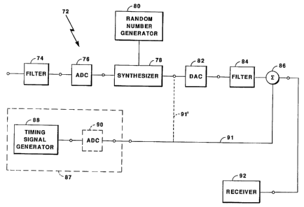
Referring now to Fig. 4 a signal encryption system 72
receives an analog signal at an input port and filters and
converts the analog signal to a first stream of bits via a
filter 74 and an ADC 76 in the same manner as described above
in conjunction with FIG. 4. Here, the bit stream is fed from
the ADC 76 to a signal encryptor 78. Here the signal
encryptor 78 receives the signals directly on separate signal
channels. A random number generator 80 is coupled to the
signal encryptor 78 and feeds a stream of random bits to the
signal encryptor 78. The random stream of bits modifies the
first bit stream to thus provide an encrypted signal. The
signal encryptor 78 combines the signals to thus provide a
reconstructed encrypted signal at an output port.
The encrypted signal is subsequently fed from the signal
encryptor 78 to an input port of a DAC 82 which converts the
encrypted bit stream to an analog signal. The analog signal
is coupled through a filter 84 which provides an
appropriately filtered signal to a first input port of a
signal combining circuit 86.
WO 94/22236 PCT/US94/02025
', x
- 24 -
A timing circuit 87 includes a timing signal generator
88 for providing a timing signal. The timing circuit 87 may
provide to a receiver 92 either an analog or a digital timing
signal and thus an optional ADC 90 is here shown coupled
between the timing signal generator 88 and the summing
circuit 86. If the DAC 90 is included in the timing circuit
90 then the timing signal is fed through optional signal path
91' to the digital input port of the DAC 8d. If the ADC 90
is omitted then the timing signal is fed through signal path
91 to the summing circuit 86 as shown.
It should be noted and those of ordinary skill in the
art will recognize that implicit in the recovery of
information at the receiving end of an analog communications
link using the analyzer and synthesizer building blocks
operating according to the above equations is the need to
synchronize the ADC in the transmitting portion of the system
and the DAC at the receiving portion of the system such that
the transmit and receive portions of the system agree on the
exact time of sampling. Large inaccuracies in
synchronization will result in gibberish out of the receiver.
Small statistical fitter in the timing synchronization will
have the same effect as noise on the link.
Timing and synchronization schemes are known to those
of ordinary skill in the art. In one method for example, an
oscillator locked to (i.e. derived from) the sampling rate
of the sending portion may be sent over the link. The
received oscillator signal may be used to derive (via phase
locked loop techniques for example) the receiver's clock
signals for sampling. As mentioned in the secure
transmitting and receiving system 40 (FIG. 3) the timing
information may be applied to the encryptor and decryptor
respectively.
In those systems employing cascade-type or tree-type
analyzers and synthesizers (FIGS. 1A - 1D) two timing signals
may be required because the inherent delay in the sending
portion of the system effectively defines "words" rather than
~'D 94/22236 PCT/US94/02025
..
- 25 -
just signal bits that should be synchronized. Such word
synchronization may be achieved by providing a second sender
oscillator which may be locked to the first oscillator
(alternatively, the first oscillator may be locked to second
oscillator thus requiring only a word synchronization) and
operating at a rate depending upon both the number of levels
in the cascade and on the type of system being provided i.e.
a signal encryptor, a signal compressor, or a modem. Such
oscillator signals may occupy the same bandwidth as the
system information, since they may be subtracted out by the
known techniques for removing a signal of known frequency and
constant amplitude. In practice these two oscillators should
preferably provide signals having a particular frequency and
a particular amplitude. In practice these two oscillators
should preferably be locked to signals having frequencies
corresponding to those frequencies which define the extreme
upper and lower band edges of the frequency bandwidth of the
system information (and the system information while still
maintaining the requirement that will not exceed the band
limits of the link.
One method for removing an interfering signal (namely,
the received oscillator signal) from the accompanying system
information signal is to form a feedback loop that subtracts
out an amount of the known (as received) frequency until the
resulting difference no longer contains any narrow band
correlation to the known (received) oscillator. The
operation of a phase locked loop includes multiplication of
an input signal with a local oscillator (which, in turn, is
locked to the received timing signal) and then integrating
the result with a low-pass filter.
' Another method for timing synchronization between the
sending .and receiving portions of the system will be
described below in conjunction with FIG. 7.
Referring now to Fig. 5 a system for transmitting
digital data over an analog medium 94 includes a modulator-
demodulator (modem) 95 here only a modulator portion of the
WO 94/22236 . PCT/US94/02025
- 26 -
modem 95 being shown. The modem 95 includes a data assembly
unit 96 for forming digital data into frames or bytes having
a predetermined length appropriately selected for data
transmission. The data assembly unit feeds the data to the
input ports of a synthesizer 98 which forms the data into a
bit stream in accordance with the technique of the sub-
synthesizer 20 described above in conjunction with FIG. 1.
That is, here digital data to be transmitted is applied to
the residual inputs W'1 ... WAN of the synthesizer. This
l0 data may be encrypted by a random number generator (not
shown) which provides an encrypting sequence which may or may
not be a secret sequence.
The synthesizer 98 feeds the bit stream into an input
port of a DAC 100, which may be provided having a nonlinear
response characteristic, which generates an analog signal
corresponding to the bit stream fed thereto. In accordance
with the Nyquist sampling theorem procedure, the digitized
samples out of the sender should be converted via the DAC 100
to an analog signal representation of the digital signal fed
thereto. The analog signal is subsequently filtered for
anti-aliasing with a filter 102 having a low pass filter
characteristic and preferably having a relatively steep
filter skirt and a cutoff frequency corresponding to one-half
the sampling rate frequency. The filtered signal is
coupled to a first input port of a summing circuit 104. A
timing circuit 106 feeds a timing signal into a second input
port of the summing circuit. The summing circuit thus
superimposes the two analog signals fed thereto.
Alternatively, a timing signal may be transmitted via the
input to the synthesizer 98.
The superimposed analog signal is transmitted over an '
analog transmission link 107 (e.g. a telephone line) to a
receiver 108 where the timing signal may be used to provide '
timing data for the receiver such that the bit stream may be
recovered from the analog signal. It is believed that a
modem constructed in accordance with the present invention
~O 94/22236 PCT/US94/02025
- 27 -
may operate at or near the maximum data rate theoretically
possible for a transmission link based on signal to noise
ratio of the link and Shannon's Law.
At the receiver 108, substantially all noise in the
frequency range above one-half the receiver sampling rate
frequency should be filtered with a filter having a low-pass
filter characteristic and having a cutoff frequency above
one-half the receiver sampling rate frequency. If the
transmission link 107 is provided as a transmission line over
l0 which signals having a frequency between 400 Hz and 3200 Hz
may be transmitted then the input signal may appropriately
be sampled at a sampling rate typically of about 6400 bps.
A single tone having a frequency typically of about 3200
Hz may be provided by the timing circuit and added to the
transmitted signal and phase-locked at the receiver as one
means of synchronizing a receiver ADC clock. Since the tone
may be provided having a known amplitude and frequency, it
may be subtracted rather than filtered out at the receiver
and thus there is no resultant loss of data.
Likewise a signal tone having a frequency typically of
about 400 Hz may be used to provide a word synchronization
for formulating the word comprising the input to all the
cascade levels. Signals in the frequency range below 400 Hz
may be used for signalling for line turnaround in a semi-full
duplex modem, for sending reverse channel data and network
information. Bits per cascade level may be increased until
the maximum power per unit of data which may be transmitted
and Shannon's limit are reached.
Furthermore error correcting codes such as M of N codes
(M redundant bits out of N) and scrambling signals may be
applied to the input data words as is known to those of
ordinary skill in the modem art.
Referring now to Fig. 6, a coded modem 110 using direct
sequence coding, in which each data word modulates all the
bits in a sequence of code bits, more than one signal may
share the link simultaneously. A shared signal SZ may be
WO 94/22236 .. PCT/US94/02025
. : . : ;:..~:1~~~44
- 28 -
provided for example, as a voice signal, television (TV)
signal or facsimile (FAX) signal or alternatively the shared
signal S2 may be provided from additional modems of the same
type operating with orthogonal code sequences.
The coded modem 110 includes a coder 112 for providing
the coding operation. The coded signal is fed to a
synthesizer 114 which provides a relatively broadband signal
having a noise-like frequency spectrum to an input port of
a summing circuit 116. A sharing signal may be fed to a
second input port of the summing circuit. The summing
circuit couples the signals fed thereto to a first end of a
transmission line 117.
At the demodulator portion, a signal tap 118 couples a
portion of the signal transmitted over the transmission line
117 to an optional signal processor 124. The signal
processor 124 feeds a processed signal to a receiver 125.
The codes of the coder 112 are selected to have good auto-
and cross- correlation properties, and thus the modem data
may be recovered even when the modem operates at low power
relative to the shared signal.
To a sharing device, the receiver 125 which may be
provided as a Tv receiver for example, the modem signal may
appear to be a small random background noise. However if the
shared signal is coupled to the TV receiver 125 through the
signal processor 124 containing the code sequences, C, then
most or substantially all of the modem "interference" in the
TV receiver 124 may be removed by known techniques for
cancelling correlated noise.
The modem 110 includes the coder 112 for providing a
coding operation C, and a decoder 122 for providing a
correlation operation, C~. In a correlation operation, data
is recovered by digitally integrating the product of the
received sequence with the stored code, C. A signal sharing
the link will typically tend to integrate to near zero since
the, shared transmission is uncorrelated to the chosen code,
~O 94/22236 PCT/US94/02025
~,
- 29 -
C. The optional interference cancellation operation for the
sharing signal is performed by the signal processor, 124.
A method for. timing synchronization between the sending
portion and receiving portion of the system 110, is now
described, however before describing the method it should be
noted that although the method may be more clearly explained
within the context of the coded modem, the method may also
be applied, with minor variations, to other systems including
the signal encryption systems described above in conjunction
with FIGS. 2-4 above and signal compression systems to be
described in conjunction with FIG. 9 below.
At least one of the signals, W'k, is forced to be a
sequence having known correlation properties. In a cascade
synthesizer, since byword" synchronization is required, the
chosen signal W'k may preferably correspond to the signal
having lowest inband sample rate. It should be noted
however, that in a direct sequence coded modem all the W'ks
are so coded.
There are many examples of suitable code sequences such
as JPL, GOLD codes and Walsh codes. For illustration and not
by way of limitation, the Walsh codes (also known as Hadamard
codes) are described. The kernal for a Walsh code is
provided as:
+1 +1
+1 -1
Higher order codes are found by substitution of a level
into the kernal as shown
+1 +1 +1 +1
+1 -1 +1 -1
+1 +1 -1 -1
+1 -1 -1 +1
which may be compactly expressed as:
+1 +1 +1 +1 - code .1
+1 -1 +1 -1 - code 2
, +1 +1 -1 -1 - code 3
+1 -1 -1 +1 - code 4
WO 94/22236 ~ ~ PCT/US94/02025
- 30 -
Many other codes, (such as the GOLD codes) are known
that have "good" correlation properties. By correlation is
meant multiplication and integration which in a two valued
binary case (+l,-1) reduces to just the vector dot product
of the sequences. A dot product between two identical codes
provides a predetermined output (i.e. (Code 1) DOT (Code 1)
- 4 ) However, a dot product between 2 unlike codes would
provide an output of zero (i.e. (code 1) DOT (codes 2,3,4,)
- 0) Similarly, this relationship also holds true for each
of the other 3 codes. Thus, these are orthogonal codes.
Non-orthogonal codes having a large auto-correlation and
a small cross-correlation may also be suitable, and some of
such codes are known to be particularly good for fast
acquisition of synchronization in a sliding correlator. An
example of a sliding correlator may be made with code 3. If
word sync is unknown (assume for this discussion that bit
sync is known) then one of four possibilities may occur in
the receiver's correlator: they are
+1 +1 -1 -1 assumed timing of the receiver's word clock
+1 -1 -1 +1 received pattern possibility 1
-1 -1 +1 +1 possibility 2
-1 +1 +1 -1 possibility 3
+1 +1 -1 -1 possibility 4
Correlation, that is the dot product of the receiver's
code with each of the 4 possible patterns reveals that the
correlator will compute a dot product of 0, -4, 0, and +4 for
each of the 4 possibilities, respectively. However, only the
correct word synchronization (i.e. namely possibility 4) will
have large positive (i.e. +4) correlation. By sliding the
receiver's assumed clock, bit by bit relative to the incoming
signal, and performing the correlation, the receiver may thus '
find word synchronization, hence the name "sliding
correlation' . Thus, it should also be noted that the maximum
correlation will occur when both the word and bit
synchronization are correct.
~O 94/22236 PCT/US94/02025
- 31 -
To accomplish the foregoing method of synchronization,
. the residual, W', of the lowest frequency stage in the
sender's cascade may be.arranged to have code 3 define its
value (or at least the sign of W' would follow code 3). The
preceding discussion illustrates some of the many ways
receiver synchronization may be achieved. In some system
applications such as encryption, the timing from the receiver
may also drive other building blocks, such as a decryptor.
In full duplex operation, a clock in the receiver may also
be used for transmission from that end such that there is
only one master clocking the system.
Assuming that bit and word synchronization have been
established in the modem 110, then an incoming data bit may
be expressed as corresponding to either +1 or -1. If that
data bit multiplies one of the codes, code 2 for example,
then the resulting 4 bit sequence is either code 2 or code
2 with the sign of each bit reversed. If that sequence is
applied to one of the W' inputs of a cascade or tree
synthesizer as a sequence of bits, then the receiver's
analyzer will recover that W' and may correlate with code 2
to get either a large positive or a large negative number
which will determine the receiver output as a +1 or a -1
respectively. Here for ease of explanation, an example using
a single bit has been described. In practical systems of
course, such operations would typically be performed on
digital words having a plurality of bits.
The application of the coded data bits to the W' inputs
of a cascade synthesizer is somewhat complicated by the fact
that each stage in the cascade operates at a different
sampling rate. Such an operation may be more easily
accomplished in a tree synthesizer since input data may be
assembled into words and applied all at once at the frequency
of the lowest synthesizer stage. For a tree synthesizer, the
transmitter's power would also be distributed more evenly
across the link bandwidth---a preferred and efficient case.
Spreading the transmitter's energy evenly across the link
WO 94/22236 , PCT/US94/02025
- 32 -
bandwidth is a prescription for possibly achieving operation
at the maximum limit of the link.
Several coded modems of the type described in Fig. 6 may
operate simultaneously over the same link, within the
constraint of total link power. Each modem should use a
different orthogonal code. For example, a code 3 modem would
not interfere with a code 2 modem. It should be noted that
the number of modems that may share a link using the 4 bit
Walsh codes described above is more than four since each
modem may have a different and unique combination of codes
on each of its independent residual inputs, provided certain
groups of modems don't operate at exactly the same time. It
should also be noted that these multiple modems may simply
be provided as different orthogonally coded data bits.
A two wire full duplex modem may be provided by using
a companion set of almost orthogonal codes. The Walsh codes
identified as code 1 through code 4 above, and their bit-wise
complement, are only one half of the 16 possible combinations
of 4-bits. As shown below the remaining combinations also
form another set of mutually orthogonal vectors, below
numbered as c5 through c8. This second set of 4 vectors is
not orthogonal to the first set. It can be described as
"nearly orthogonal" because the dot product of any member of
set 1 with any member of set 2 is always half the length of
the vector; and of course the dot product of any member with
another of the same set is always 0 except that the product
with itself is always equal to the length.
MASTER (set 1) SLAVE (set 2)
c1 = + + + + C5 = + - - - - c1-
3 0 c2 = + - + - c6 = + + - + = C2 ~
C3 = + + - - C7 = + - + + = c3 ~
c4 = + - - + c8 = + + + - - c4 ~
The master group is orthogonal and the slave group is
also orthogonal, however the cross group correlation is -2
for the dual and +2 for any other cross term. One end of a
94/22236 p
C~l~ PCT/US94/02025
- 33 -
transmission link may transmit signals using the master set
of codes and a second end of the transmission link may
transmit using the slave set of codes. It should be
noted that the same benefits may be realized by using the
matrix transformation approach to provide the synthesizer 114
and analyzer 120.
Thus to provide full duplex operation, the modems at
each end of a link can be assigned to use set 1 or set 2 as
Master and Slave. If the Master used only codes 1 and 2 and
the Slave used codes 3 and 4 then all echo signals would be
totally cancelled by the orthogonality but the data
throughout for each modem would be half of the rate possible
by using the arrangement described above based on the two
sets of codes.
Furthermore, coded modems of the type described in
conjunction with Fig. 6 may coexist with other signals on the
link since the correlator will provide little or no output
signal. Longer code sequences may improve this effect at
the expense of lower data throughput. Certain codes, other
than the Walsh codes, may be better able to exploit this
characteristic for multiple access applications.
For a modem 126 as shown in Fig. 7, it is possible to
use direct sequence code division multiplexing to excite the
sub-stages of the synthesizer cascade. As described above,
such a procedure would permit clock recovery based on a
sliding correlation. It also allows data multiplying the
code sequence (as is done in direct sequence spread spectrum)
to be recovered at a receive end using correlation
techniques.
One application for such a coded modem would be to take
advantage of the processing gain of the correlation receiver
to recover a low power signal from the modem buried in a
large "jamming" signal. Practical examples of jamming
signals include voice (hence data may be sent as 'noise'
under the voice), television (hence high definition digital
information may be sent in the same channel as standard video
WO 94/22236 , ~ ~ ~ ~ ~ PCT/US94/02025
- 34 -
to maintain compatibility), code division multiplexing and
two wire full duplex FDX. The disclosed technique is an
improvement on those methods because the modem utilizes the
bandwidth more efficiently than heretofore.
Furthermore, the modem described herein, being a
modulator (the synthesizer) and a demodulator (the analyzer)
may also take the form of a baseband RF or soundwave
transmitter modulator and receiver (or above baseband except
for the limits of ADC's). Such a receiver may have
application in receiving digital High Definition TV (HDTV).
Coded modems of the type described above in conjunction
with FIG. 6 and to be described in conjunction with FIG. 7
below may use Walsh codes to pre-encode data which is applied
to the w° and v' inputs. Because the synthesizer itself uses
Walsh codes, if implemented by the rotation matrix, it should
be pointed out that these two coding schemes are independent.
For example, the code length for the data inputs need not be
the same as the number of synthesizer outputs. The number
of outputs is equal to the length of the synthesizer rotation
operators. Thus by applying the matrix method to the coded
modem, the coded modem becomes in essence a twice coded
modem.
Referring now to Fig. 7, a coded tree modem 126 includes
a plurality of coder circuits 128a - 128h coupled to
corresponding ones of a plurality of input ports 130a - 130h
of a tree-type synthesizer 130 operating in accordance with
the principles described above in conjunction with FIG. 1.
The synthesizer output port is coupled through a link 132 to
an input port of a tree-type analyzer 134 also operating in
accordance with the principles described above in conjunction
with FIG. 1. A plurality of decoder circuits 136a - 136h are
coupled to the analyzer output ports 134a - 134h to decode
the coded signals fed thereto.
In principal the coded tree modem 126 operates such that
the,coder circuit performs a coding operation of multiplying
a data word times an orthogonal code C. The decoder performs
~O 94/22236 ~ ~ PCT/US94/02025
- 35 -
a correlation operation here denoted C~. It should be noted
that the final V~ input sequence on line 130h may be set to
zero if it is assumed to be below a frequency corresponding
to the lower frequency limit of the passband frequency of the
link 132.
Referring now to Fig. 8, a system for transmitting and
receiving compressed signals 138 includes a transmit portion
138a having an input signal conditioning circuit 139, which
here includes an input filter 140 and an ADC 142. The filter
140 and ADC 142 are selected to operate in accordance with
the techniques described above to provide an appropriate
stream of digital words to the first input port of an
analyzer 144. A quantizer 146 is coupled between the
analyzer 144 and a synthesizer 148. In operation, the signal
compressor quantizer 146 maps the residual W~(N) into a new
number taking fewer bits to describe. Thus it is a
compression operation.
An output signal conditioning circuit 149 includes a DAC
15o coupled to the output port of the synthesizer 148. The
DAC 150 receives a digital stream of words and provides an
analog output signal representative of the bit stream fed
thereto. A filter 152 having appropriately selected filter
characteristics couples the analog signal from the DAC 150
to a first end of a transmission line 154.
A second end of the transmission line 154 is coupled to
a receive portion 138b of the system 138. The receive
portion b includes an input signal conditioning circuit 156,
which appropriately filters and converts the analog signal
fed thereto to provide an appropriate stream of digital words
to the first input port of an analyzer 158. An inverse
quantizer 160 (i.e requantizer) is coupled between the
analyzer 158 and a synthesizer 162.
In operation, the requantizer 160 remaps to the original
bit definition. The compression operation, of course, lowers
the, information content of the signal and that lost
information may not be recovered. In many applications,
WO 94/22236 PCT/US94/02025
,s, , r
- 36 -
however, the lost information is redundant or the human
observer is insensitive to the level of detail contained in
the information discarded by the quantizer and thus little
or no signal degradation may be detected.
An output signal conditioning circuit 163 receives a
reconstructed digital stream of words from the synthesizer
162 and provides an appropriately filtered analog output
signal representative of the bit stream fed thereto to an the
output port of the receive portion 138b of the system.
In speech compression processes, bandwidth may generally
be reduced by limiting the number of bits devoted to the
residual W'.
However, an alternative which may provide an increased
reduction in bandwidth may be accomplished by f first replacing
a signal VS on the cascade channel corresponding to the
lowest frequency band with a zero, thus only transmitting the
signal W'S. Next, a signal W'3 associated with a cascade
channel corresponding to the frequency band in the 700 Hz to
1400 Hz frequency range may be eliminated or coarsely
quantized. Furthermore, Huffman coding or codebook vector
quantization methods may be used on W'2.
By adjusting the sample rate, the frequency band from
700 Hz to 1400 Hz may be isolated. Since human voice
especially in the English language, generally does not
include a formant in this range, the cascade channel
corresponding to the frequency band from 700 Hz to 1400 Hz
may be eliminated (i.e. by setting the residual W'3 equal to
zero) with little loss in intelligibility. Similarly, as
shown in the Table below, W'1 and W'S may also be set to zero.
~O 94/22236 _ ~ PCT/US94/02025
- 37 -
TABLE
IGNAL SAMPLE RATE ~(samples/second) FILTER RANGE
Hz
W'1 5600 W'1 =0 2800 to
3200
W'2 2800 W'2 1400 to 2800
W's 1400 W'3 =0 700 to
1400
W'4 700 W'4 350 to 700
Was 350 W's =0 175 to
350
Vs 17 5 Vs =0
Thus, in this example W'1 through W's and Vs are sampled
at the rates shown in the Table and it is possible to
transmit only the signals corresponding to the residuals W'
2
and W'4, for example, which have sample rates of 700 and 2800
baud perhaps less than 2 bits for each residual W'
W'
after
2,
4
Huffman coding. Further reduction may also be possible since
W'2 may simply be considered as another sampled signal and
thus may also be subdivided by multiresolution analysis to
further reduce the bandwidth.
By way of example, if 1.5 bits are used for the 700
sample/second residual and W'Z is decomposed into 1400
samples/second, 700 samples/second, 350 samples/second, 175
samples/second, and 65 samples/second at 1.5 bits each then
the total number of bits per second (bps) corresponds to
5085 bps to which should be added overhead bits for frame
synchronization. This method is considerably less
computationally complex than methods such as Linear
Prediction Coding 10 (LPC10) and dynamic Excitation LPC and
refinements thereto as are known to those or ordinary skill
in the art of voice compression.
Although not here shown, the receiver may be provided
having the same form with received signal applied to Vo and
the clear output taken from V'o.
In view of the above, those of ordinary skill in the art
will now recognize that combinations of the system described
WO 94/22236 PCT/US94/02025
.. .
- 38 -
above may be created to form, for example, an encrypted data
compression system for use on analog links. This may be
particularly useful, for example, in those applications such
as transmission and reception of high definition television
signals in which the amount of digital data to be transmitted
exceeds the Shannon Law limit of the link. Thus, in such
applications the data may first be compressed by any
algorithmic means until the sample rate is consistent with
the Nyquist sampling theorem limit of the link and the data
may then be applied to one of the modem systems described
hereinabove in conjunction with FIGs. 5-7 for example.
Referring now to FIG. 9, a digital compression circuit
166 includes an analyzer 168 coupled to a quantizer 170. A
digital signal is fed to the analyzer input. The analyzer
168 decomposes the signal and the quantizer 170 performs a
compression operation as described above in conjunction with
FIG. 8. The quantizer 170 subsequently feeds a compressed
digital signal to a first end of a digital link 172. A
second end of the digital link 172 is coupled to an input
port of a requantizer 174. The requantizer 174 receives the
signal fed thereto performs an inverse quantization process
and subsequently feeds a requantized signal to a synthesizer
176. For a digital scheme it is only necessary to perform
a logical operation, such as an exclusive or operation,
between the W signal and a random number RN.
Referring now to FIG. 10, a telephone modem 178 includes
a synthesizer 180, capable of operation over the frequency
band from 400 Hz to 3200 Hz. The synthesizer 180 feeds a
signal to a DAC 182 having a sampling rate typically of about
6400 samples/second which converts the bit stream fed thereto
to an analog signal. The analog signal is subsequently fed
over an analog transmission link 184 to an ADC 186 also
having a sampling rate typically of about 6400
samples/second. The ADC 186 converts the analog signal fed
thereto to a digital bit stream. The digital bit stream is
subsequently fed to an analyzer 188.
~O 94/22236 PCT/US94/02025
- 39
The synthesizer 180 may be provided in accordance with
the matrix transformation methods described above in
conjunction with FIG. 1. It should be noted, however, that
the synthesizer 180 may alternatively be provided as a three
level tree synthesizer in accordance with Equations 3 and 4
also described above in conjunction with FIG. 1.
In the matrix approach, the synthesizer 180 operates on
the data frames fed thereto with a rotation matrix. Here,
an 8 dimensional rotation matrix would be applied to the data
frames. Similarly, the analyzer 188 would perform an inverse
rotation operation by applying an 8 dimensional matrix
corresponding to the inverse matrix of the matrix used by the
synthesizer 180.
As mentioned above, the basic sampling rate of 'the DAC
182 and ADC 186 is 6400 samples/sec. The digital input and
output operate at a frame rate of 1/8 or 800 frames per
second. Each frame may be composed, for example, of 35 bits
divided into 7 words of 5 bits (or more) each and applied to
channels 180a - 180h. The thruput is 28, 000 bps (35 bits
times 800 frames/second). The usable rate is determined by
the S/N ratio on the link 184 and forward error correction
~(FEC). Thus, the modem 178 may operate at a data transfer
rate at or below 28 kbps.
Furthermore, the modem 178 may utilize FEC and as is
common practice, the frequency range from 300 Hz to 400 Hz
may be used for frequency shift keying (FSK) diagnostic
signalling.
Channel 180h corresponds to signaling below 400hz and
cannot be used for data in this example. However, if a
signal having a constant amplitude and alternating sign is
applied to channel 180h then a 400hz tone may be filtered
from the line signal by a receiver (not show
t
i
n)
o a
d in
. , synchronization. In addition, the known preselected
amplitude may be recovered from channel 188h as data and used
as a gain calibration signal in the receiver and, may further
WO 94/22236 " ~ PCT/US94/02025
- 40 -
be used to define block boundaries for FEC block coding
schemes.
Accurate timing synchronization and gain calibration are
important to the operation of the modem 178. As described
above in conjunction with FIGS. 6 and 7, coded modems may
obtain synchronization information without any tones
appearing in the transmitted signal. Thus, clandestine
communications by encrypting coded modems may be transmitted
as low level, seemingly uncorrelated, noise in the same
narrow bandwidth as simultaneous, non secret, communications.
The data in the channels 180a - 1808 may be scrambled,
as is common practice in modems, so that the output appears
more noise-like when transmitting the commonly encountered
input string of 35 zeros or ones. Without scrambling, an
input string of zeros will produce a modulated but strongly
correlated output without a DC component.
The data received by the analyzer 188 will be a multiple
of the actual data. The multiplication factor will
correspond to the dimension of the rotation matrix which in
turn corresponds to the number of channels in the synthesizer
180. The receiver should quantize, that is, round the
received channel output to the nearest multiple then divide
by the multiple to reduce the effects of noise on the link
184.
. A modem using baseband modulation techniques, in which
no carrier signal exists, may also be provided by using the
matrix rotation approach or by the equations provided in
conjunction with FIGS. 1-1D above. In either of these
approaches, the modem must demodulate and process groups of
two or more samples to recover the data. In a conventional
baseband system, single samples are processed to recover the
data.
Thus, in a baseband system a modem operating according
to the matrix method described above should modulate and
demodulate groups of samples. For example, if the matrix
vectors are of length eight, then eight samples should be
~O 94/22236 PCT/US94/02025
- 41 -
processed together as an independent group by the
demodulator. That is, the demodulator multiplies the group
of samples by the inverse matrix used in the modulator. It
should be noted that the grouping of samples is part of the
modulation and distinct, for example, from a block data
coding method for error correction, and both techniques may
be simultaneously used in a single modem.
Having described preferred embodiments of the invention,
it will now become apparent to one of ordinary skill in the
art that other embodiments incorporating the concepts may be
used. It is felt, therefore, that these embodiments should
not be limited to disclosed embodiments but rather should be
limited only by the spirit and scope of the appended claims.