Note: Descriptions are shown in the official language in which they were submitted.
21~~6~~
A METHOD AND APPARATUS FOR COMMUNICATION AND SIGNAL
SYNTHESIS
BACKGROUND OF THE INVENTION
FIELD OF THE INVENTION
The present invention relates to a communication
apparatus applying a frequency synthesizer wherein a
direct digital synthesizer is used. Particularly, this
invention relates to downsizing and a high precision
receiving/transmitting apparatus and a frequency
synthesizer used in radio communications systems.
DESCRIPTION OF THE RELATED ART
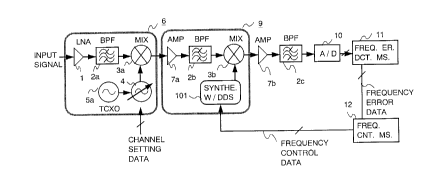
Fig. 48 shows an example configuration of a
conventional receiving apparatus constructed based on a
receiving apparatus including an auto frequency control
(AFC) circuit. The receiving apparatus including the
auto frequency control circuit is disclosed in "TDMA
Communication" by Heiichi Yamamoto et al Institute of
Electronics and Communication pp. 87-89, Spring
Conference B-198 of Electronics Information Communication
Institute in 1993, Unexamined Japanese Patent Publication
3-284016) Unexamined Japanese Patent Publication 3-
1
21~86~~
296318, and Unexamined Japanese Patent Publication 4-
156712.
In Fig. 48, a low noise amplifier (LNA) 1, band pass
filters (BPF) 2a) 2b and 2c, mixers (MIX) 3a and 3b, a
phase locked loop (PLL) synthesizer 4, a temperature
compensation quartz-crystal oscillator (TCXO) 5, a
frequency converter 6 for high frequency, amplifiers
(AMP) 7a and 7b, a voltage-controlled quartz-crystal
oscillator (VCXO) 8) a frequency converter 9 for low
frequency, an analog-digital converter (A-D converter)
10, a frequency error detecting means 11) a frequency
control means 12, a memory 13, and a digital-analog
converter (D-A converter) 14 are provided. The frequency
converter 6 for high frequency includes the LNA 1, the
BPF 2a, the MIX 3a, the TCXO 5 and the PLL synthesizer 4.
An output frequency of the PLL synthesizer 4 is
controlled based on channel setting data. A receiving
frequency is set based on the controlled output frequency
from the PLL synthesizer 4. The frequency converter 9
for low frequency includes the AMP 7a) the BPF 2b. the
MIX 3b and the VCXO 8. The receiving frequency can be
adjusted finely based on a control voltage applied at the
VCXO 8.
The operation will now be described. In the
conventional receiving apparatus shown in Fig. 48, a
2
21~86~~
frequency of an input signal is changed to an
intermediate frequency (IF) signal of a predetermined
frequency through the frequency converter 6 for high
frequency and the frequency converter 9 for low
frequency. The changed frequency is amplified at the AMP
7b and filtered at the BPF 2c. By this procedure, other
input signals of neighboring frequencies are suppressed.
The filtered frequency is converted from analog to
digital at the A-D converter 10. In a common receiving
apparatus for digital communication, an input signal
expressed in digital amount is demodulated by digital
operation and a transmission signal is extracted. In
this case, there is a difference between a center
frequency of the input signal and a receiving frequency
in the receiving apparatus. This frequency difference is
hereinafter called a frequency error. If the frequency
error increases, the modulation performance (bit error
rate in a digital transmission method) is gradually
deteriorated. If the frequency error increases too far,
it becomes impossible to receive the input signal because
the input signal is defined to be out of passing
bandwidth of the BPF 2c. The phenomenon, such as the
above, becomes distinctive especially in a slow
transmission speed system, such as a single channel per
carrier (SCPC) method wherein speech transmission is
3
21~866~
mainly treated.
' Generally, in the receiving apparatus as shown in
Fig. 48, the frequency error is detected by the frequency
error detecting means 11, a frequency of the VCXO 8 is
controlled, and the frequency error is corrected in
addition to the modulation operation. Based on frequency
error data obtained by the frequency error detecting
means 11, frequency control data is calculated for the
purpose of correcting the frequency error in the
receiving frequency by the frequency control means 12.
The memory 13 is accessed based on the frequency control
data. A table for output frequency of the VCXO 8 vs.
control voltage, or a table for increased amount of the
output frequency of the VCXO 8 vs. increased amount of
the control voltage is stored in this memory 13. Voltage
data applied at the VCXO 8 is output from the memory 13
based on the frequency control data. The voltage data is
converted to the control voltage for the VCXO 8 at the D-
A converter 14. The above serial controlling of the
frequency is called AFC. (auto frequency control)
Fig. 49 shows a configuration of the PLL synthesizer
4. A variable divider 15, a reference signal divider 16,
a phase comparator 17, a loop filter 18, a voltage-
controlled oscillator (VCO) 19) the temperature
compensation quartz-crystal oscillator (TCXO) 5 and a PLL
4
21~86~7
34 are shown in Fig. 49. The temperature compensation
quartz-crystal oscillator (TCXO) 5 is a reference
oscillator. A frequency of output signal of the VCO 19
is divided by dividing ratio N in the variable divider
15. A frequency of output signal of TCXO 5 is divided by
dividing ratio R in the reference signal divider 16. The
PLL operates in order to make the above divided
frequencies be coincident. Accordingly, output frequency
fout of the PLL 34 is N/R times output frequency fxo of
TCXO 5 (fout = (N/R) ~ fxo). The output frequency fout
of the PLL synthesizer 4 can be switched by interval
fxo/R. The output frequency fout can be switched by
changing dividing ratio N of the variable divider 15.
The dividing ratio N is changed by the channel setting
data.
Other configurations of the PLL synthesizer 4 are
shown in Fig. 50 and United States Patent US4965533. The
configuration of Fig. 50 is described in the paper, A. L.
Bramble) "Direct Digital Frequency Synthesis") IEEE 35th
Ann. Frequency Control Symposium, May 1981, pp. 406 -
414.
In Fig. 50, a direct digital synthesizer (DDS) 31, a
reference clock 32 and a frequency divider 33 are shown.
The DDS 31 synchronized with the reference clock 32 is
used as a reference oscillator of PLL 34) in this PLL
5
21~~6~~
synthesizer 4.
Fig. 51 shows a configuration of the DDS 31. A
phase accumulator 40) a memory 41) a digital-analog
converter 42 and a filter 43 are shown in Fig. 51.
Frequency data ( A~ ) represented by plural bits is input
and accumulated at the phase accumulator 40 in the DDS
31. The accumulated data is converted to phase data
and output. Amplitude data sin ~ of a sine wave is
stored in the memory 41 in advance. The amplitude data
sin ~ of a sine wave is output based on the phase data ~.
The output data is converted to analog waveform at the D-
A converter 42. The above digital operation is performed
synchronous with the reference clock. Output from the D-
A converter 42 is input into the filter 43. Spurious
components of the reference clock) higher harmonic and so
forth is removed at the filter 43. High-frequency
resolution can be easily obtained by increasing the
number of bits of the frequency data ( A~ ), without
deteriorating other characteristics, in DDS 31.
Accordingly, high-frequency resolution also can be
obtained in the PLL 34 whose reference oscillator is the
DDS 31.
Fig. 52 shows another configuration of the DDS 31.
In this DDS 31, a sin ~ operation circuit 44 is provided
instead of the memory 41. The sin ~ calculation circuit
6
21~~~~~
44 is provided in order to avoid making the capacity of
the memory 41 large when the high-frequency resolution is
obtained by increasing the number of bits of the
frequency data ( A~ )in the DDS 31. CORDIC algorithm and
so forth is used in the sin ~ calculation circuit 44.
The amplitude data sin ~ of a sine wave is obtained by
digital operation.
There are many disadvantages to the conventional
receiving apparatus. For example, when a narrow
bandwidth digital transmission of low symbol speed is
performed for transmitting speech in SCPC (single channel
per carrier), it is necessary to enhance the frequency
setting accuracy at AFC. The reason is that the BPF 2c
becomes a narrow band. The receiving frequency is finely
adjusted by treating the frequency control data through
the D-A converter 14, the memory 13 and the VCXO 8, in
the conventional receiving apparatus. The VCXO 8 has a
configuration wherein a varactor diode is connected to a
quartz-crystal resonator for modulating the frequency.
Thus sensitivity of the modulation is changed depending
upon control voltage. Therefore, in order to enhance the
frequency setting accuracy, it is needed to increase the
number of entries for a table of output frequency vs.
control voltage stored in the memory 13 for enhancing the
resolution. This increase introduces a problem of a
7
2158667 ~~~
larger memory 13 requirement.
In addition, an output frequency of the VCXO 8 and
the modulation sensitivity of the VCXO 8 are changed
depending upon temperature. Therefore, it has another
problem that the frequency setting accuracy is
deteriorated with temperature variations.
Moreover, characteristics of the VCXO 8 relating to
output frequency vs. control voltage differs depending
upon each VCXO. In order to set the frequency highly
accurately, it is necessary to measure the characteristic
data of output frequency vs. control voltage for each
receiving apparatus and to write the data into the
memory 13. This rewriting procedure introduces another
problem of higher cost.
As one of solutions for the above problems relating
to the AFC, the following method is introduced. A
digital oscillator is described in the book, "Digital
Mobile Communication", edited by Syuji Kuwahara, Kagaku
Syuppan, pp. 269-271 published September 1992 by Kagaku
Shimbun-Sha (Japan). The method for the solution is to
correct a frequency error by a digital operation using
the digital oscillator. Fig. 53 shows a configuration of
the method.
A demodulator 35 and a digital oscillator 36 are
shown in Fig. 53. It is easy to enhance the frequency
setting accuracy according to this configuration.
8
However, this method can not be applied when the
frequency error is large and thus when an input signal is
out of the passing bandwidth of the BPF 2c.
Problems in applying the VCXO 8 to the AFC in the
receiving apparatus have been described. A similar
configuration is also used for a transmitting apparatus
in order to control a transmitting frequency. Namely, a
transmitting frequency error is calculated based on a
receiving frequency error. The VCXO 8 used as a local
oscillator for the transmitting apparatus is controlled
depending upon the transmitting frequency error. In this
case also, there is the problem that the amount of the
memory 13 becomes large in enhancing the frequency
setting accuracy because the VCXO 8 is used. There is
also the problem that a desired frequency setting
accuracy can lead to high cost.
Now, the problem of the conventional PLL synthesizer
shown in Fig. 49 when being applied in the receiving
apparatus will be described.
Generally, phase comparison frequency fr (fr - fxo /
R) of the PLL synthesizer wherein a frequency is switched
by a variable divider is the same as a channel frequency
interval. Therefore, the phase comparison frequency fr
of the PLL synthesizer becomes low frequency in a system
wherein the frequency interval of the channel is narrow,
9
21~86~'~
such as SCPC method of low transmission speed. In this
case, phase noise PN close to a carrier wave of the PLL
synthesizer increases, which brings about a problem that
communication quality and selecting receiving frequency
accuracy are deteriorated. The phase noise PN close to
the carrier wave of the PLL synthesizer can be obtained
in the following equation.
PN = 10 ~ LOG1~{ (fout/fr)Z ~ (1/2) ~ (Ef/Kp)2}
(dBc/Hz) (1)
In the equation, fout is output frequency of the PLL
34, Ef is noise voltage for input conversion for the loop
filter and, Kp is signal detection sensitivity of the
phase comparator 17. When the phase comparison frequency
fr becomes low frequency, loop bandwidth of the PLL 34
also becomes narrow. Therefore, response speed of the
PLL 34 becomes slow, which brings about a problem that
the frequency switching time becomes long.
The PLL synthesizer 4 wherein the DDS 31 is used as
a reference oscillator of the PLL 34, shown in Fig. 50)
has been introduced to improve the above disadvantages.
The variable divider 15 is not used in this PLL
synthesizer 4 because the frequency is changed by the DDS
31. Therefore, it is possible to optionally select the
phase comparison frequency fr. In addition, since a
frequency is changed by the DDS 31, a frequency of narrow
215~6~'~
channel can be easily obtained without deteriorating the
characteristics relating to the phase noise and the
frequency switching time and so forth. Namely, the
problems of increasing phase noise and lengthening
frequency switching time can be solved. However, there
is a problem that spurious components caused by a
quantization error is high because the DDS 31 generates a
sine wave by digital operation.
Fig. 54 shows an example of an output spectrum of
the DDS 31. The spurious component is amplified in the
passing bandwidth in the PLL 34. Assuming that the
spurious component of the DDS 31 is SPdds (dBc) and the
spurious component of the output signal from the PLL
synthesizer 4 is SPout (dBc), the relation between these
two can be obtained in the following equation.
SPout - 10 ~ LOG1~ ( fout/f r ) Z + SPdds
- 10 ~ LOG1~(N)Z + SPdds
(dBc) (2)
The spurious component in such a configuration of
the PLL synthesizer is high) which brings about a problem
that the communication quality and the frequency
selecting accuracy are deteriorated. Therefore, the
output frequency fout applied to such PLL synthesizer is
relatively restricted to be a low frequency.
Though there is a method of increasing the output
11
21~~6~7
frequency (phase comparison frequency ) fr of the DDS 31
in order to solve the above problems, this method has
another problem. The problem is that electrical power
consumption increases in proportion to an operating
frequency as shown in Fig. 55.
SUMMARY OF THE INVENTION
A communications apparatus comprises
a first frequency converter for shifting a first
frequency characteristic of a first signal by a shift
frequency interval to provide a second signal having a
second frequency characteristic, the first frequency
converter includes
a direct digital synthesizer for generating a
shifting signal that defines the shift frequency
interval, and
a mixer, operatively connected to the direct
digital synthesizer, for mixing the shifting signal and
the first signal,
a frequency error detector, operatively connected to
the first frequency converter, for determining a
frequency error between the second frequency
characteristic and a predetermined frequency
characteristic, and
12
2m~ss~
a frequency controlling unit, operatively connected
to the frequency error detector and the first frequency
converter, for readjusting the shift frequency
interval based on the frequency error.
A communications apparatus comprises
a receiving frequency converter for inputting an
input signal and for generating a first signal having a
first frequency characteristic by mixing a filtered
component of the input signal with a receiving signal,
a first frequency converter, operatively connected
to the receiving frequency converter, for shifting the
first frequency characteristic of the first signal
by a first shift frequency interval to provide a received
signal,
a second frequency converter for shifting a second
frequency characteristic of a second signal by a second
shift frequency interval,
a transmitting frequency converter, operatively
connected to the second frequency converter, for
generating an output signal by mixing the second signal
with a transmitting signal,
a direct digital synthesizer, operatively connected
to the first frequency converter and the second frequency
converter, for generating a first shift signal that
defines the first shift frequency interval and a second
13
215~6~~~
shift signal that defines the second shift frequency
interval,
a frequency error detector, operatively connected to
the first frequency converter and the second frequency
converter, for determining a first frequency error
between the first frequency characteristic and a first
predetermined characteristic and for determining a second
frequency error between the second frequency
characteristic and a second predetermined frequency
characteristic, and
a frequency controlling unit) operatively connected
to the frequency error detector, the first frequency
converter, and the second frequency converter, for
readjusting the first shift frequency interval based on
the first frequency error and for readjusting the second
shift frequency interval based on the second frequency
error.
A frequency synthesizer for generating a final
signal having a predetermined frequency characteristic,
the frequency synthesizer comprises
a direct digital synthesizer for generating a first
signal having a first frequency characteristic determined
by first channel setting data and having a first
amplitude,
a first divider, operatively connected to the direct
14
21~86~~
digital synthesizer, for dividing the first frequency
characteristic of the first signal to generate a divided
signal having a divided frequency characteristic,
a frequency converter, operatively connected to the
first divider, for shifting the divided frequency
characteristic by a shift frequency interval to provide a
reference signal having a reference frequency
characteristic, and
a phase locked loop for generating the final signal
from the reference signal.
A frequency synthesizer for generating a final
signal having a predetermined frequency characteristic,
the frequency synthesizer comprises
a direct digital synthesizer for generating a first
signal having a first frequency characteristic determined
by channel setting data,
a first phase locked loop, operatively connected to
the direct digital synthesizer, for generating a
reference signal from the first signal, and
a second phase locked loop) operatively connected to
the first phase locked loop for generating the final
signal from the reference signal.
A method for communicating with signals at a
predetermined frequency characteristic, the method
comprises the steps of
218667
generating a shifting signal that defines a shift
frequency interval, with a direct digital synthesizer,
shifting a first frequency characteristic of a first
signal by the shift frequency interval, by mixing the
first signal with the shift signal, to provide a
second signal having a second frequency characteristic,
detecting a frequency error between the second
frequency characteristic and the predetermined frequency
characteristic, and
adjusting the shifting signal to change the shift
frequency interval based on the frequency error.
A method for synthesizing a final signal having a
predetermined frequency characteristic, the method
comprises the steps of
generating a first signal, having a first frequency
characteristic determined by first channel setting data
and having a first amplitude, at a direct digital
synthesizer,
dividing the first frequency characteristic of the
first signal to generate a divided signal having a
divided frequency characteristic,
shifting the divided frequency characteristic by a
shift frequency interval to provide a reference signal
having a reference frequency characteristic) and
generating the final signal from the reference
16
21586~~
signal, at a phase locked loop.
A communications apparatus comprises
a first frequency converter for shifting a first
frequency characteristic of a first signal by a shift
frequency interval to provide a second signal having a
second frequency characteristic,
a frequency error detector, operatively connected to
the first frequency converter, for determining a
frequency error between the second frequency
characteristic and a predetermined frequency
characteristic, and
a means for readjusting the shift frequency interval
based on the frequency error using digital operations.
A frequency synthesizer for generating a final
signal having a predetermined frequency characteristic,
the frequency synthesizer comprises
a means for generating a first signal having a first
frequency characteristic by digital operations and
determined by first channel setting data,
a first divider, operatively connected to the means
for generating, for dividing the first frequency
characteristic of the first signal to generate a divided
signal having a divided frequency characteristic,
a frequency converter, operatively connected to the
first divider, for shifting the divided frequency
17
21~~6~~
characteristic by a shift frequency interval to provide a
reference signal having a reference frequency
characteristic, and
a phase locked loop for generating the final signal
from the reference signal.
Other objects, features, and advantages of the
invention will be apparent from the following description
when taken in conjunction with the accompanying drawings.
BRIEF DESCRIPTION OF THE DRAWINGS
Fig. 1 shows a block diagram of one example of a
receiving apparatus according to Embodiment 1 of the
present invention;
Fig. 2 shows a block diagram of one example of a
synthesizer with DDS according to Embodiment 1 of the
present invention;
Fig. 3 shows a block diagram of another example of a
receiving apparatus according to Embodiment 1 of the
present invention;
Fig. 4 shows a block diagram of another example of a
receiving apparatus according to Embodiment 1 of the
present invention;
Fig. 5 shows a block diagram of another example of a
receiving apparatus according to Embodiment 1 of the
18
2i58~6'~
present invention;
Fig. 6 shows a chart relating to operation of DDS
according to Embodiment 1 of the present invention;
Fig. 7 shows a chart relating to phase data and
amplitude data of DDS according to Embodiment 1 of the
present invention;
Fig. 8 shows a block diagram of one example of a
transmitting apparatus according to Embodiment 1 of the
present invention;
Fig. 9 shows a block diagram of one example of a
receiving apparatus according to Embodiment 2 of the
present invention;
Fig. l0A shows a chart relating to channel setting
data according to Embodiment 2 of the present invention;
Fig. lOB shows another chart of channel setting data
according to Embodiment 2 of the present invention;
Fig. 11 shows a block diagram of another example of
a receiving apparatus according to Embodiment 2 of the
present invention;
Fig. 12 shows a block diagram of one example of a
transmitting apparatus according to Embodiment 2 of the
present invention;
Fig. 13 shows a block diagram of an example of a
receiving apparatus according to Embodiment 3 of the
present invention;
19
21~866'~
Fig. 14 shows a block diagram of another example of
a receiving apparatus according to Embodiment 3 of the
present invention;
Fig. 15 shows a block diagram of one example of a
transmitting apparatus according to Embodiment 3 of the
present invention;
Fig. 16 shows a block diagram of an example of a
receiving apparatus according to Embodiment 4 of the
present invention;
Fig. 17 shows a block diagram of one example of a
transmitting apparatus according to Embodiment 4 of the
present invention;
Fig. 18 shows a block diagram of an example of a
receiving apparatus according to Embodiment 5 of the
present invention;
Fig. 19 shows a block diagram of one example of a
transmitting apparatus according to Embodiment 5 of the
present invention;
Fig. 20 shows a block diagram of one example of a
receiving/transmitting apparatus according to Embodiment
6 of the present invention;
Fig. 21 shows a block diagram of another example of
a receiving/transmitting apparatus according to
Embodiment 6 of the present invention;
Fig. 22 shows a block diagram of one example of a
21~~~~7
receiving/transmitting apparatus according
to Embodiment
7 of the present invention;
Fig. 23 shows a block diagram of another example of
a receiving/transmitting apparatus according to
Embodiment 7 of the present invention;
Fig. 24 shows a block diagram of an example of a
receiving/transmitting apparatus according
to Embodiment
8 of the present invention;
Fig. 25 shows a block diagram of an example of a
receiving/transmitting apparatus according
to Embodiment
9 of the present invention;
Fig. 26 shows a block diagram of an example of a
frequency synthesizer according to Embodiment 10 of the
present invention;
Fig. 27 shows a block diagram of another example of
a frequency synthesizer according to Embodiment 10 of
the
present invention;
Fig. 28 shows a block diagram of another example of
a frequency synthesizer according to Embodiment 10 of
the
present invention;
Fig. 29 shows a block diagram of an example of a
frequency synthesizer according to Embodiment 11 of the
present invention;
Fig. 30 shows a block diagram of an example of a
frequency synthesizer according to Embodiment 12 of the
21
21~~6~'~
present invention;
Fig. 31 shows a block diagram of another example of
a frequency synthesizer according to Embodiment 12 of the
present invention;
Fig. 32 shows a block diagram of another example of
a frequency synthesizer according to Embodiment 12 of the
present invention;
Fig. 33 shows a block diagram of another example of
a frequency synthesizer according to Embodiment 12 of the
present invention;
Fig. 34 shows a block diagram of an example of a
frequency synthesizer according to Embodiment 13 of the
present invention;
Fig. 35 shows a chart relating to a characteristic
of PLL of a frequency synthesizer according to Embodiment
13 of the present invention;
Fig. 36 shows a block diagram of an example of a
frequency synthesizer according to Embodiment 14 of the
present invention;
Fig. 37A shows a chart relating to operation of a
level converter used for a frequency synthesizer
according to Embodiment 14 of the present invention;
Fig. 37B shows another chart relating to operation
of a level converter used for a frequency synthesizer
according to Embodiment 14 of the present invention;
22
21~~6~~
Fig. 38 shows a block diagram of an example of a
frequency synthesizer according to Embodiment 15 of the
present invention;
Fig. 39A shows a chart relating to an output
spectrum of a frequency synthesizer according to
Embodiment 15 of the present invention;
Fig. 39B shows another chart relating to an output
spectrum of a frequency synthesizer according to
Embodiment 15 of the present invention;
Fig. 39C shows another chart relating to an output
spectrum of a frequency synthesizer according to
Embodiment 15 of the present invention;
Fig. 40 shows a block diagram of an example of a
frequency synthesizer according to Embodiment 16 of the
present invention;
Fig. 41 shows a block diagram of an example of a
loop filter used in a frequency synthesizer according to
Embodiment 16 of the present invention;
Fig. 42A shows a chart relating to a characteristic
of a loop filter used in a frequency synthesizer
according to Embodiment 16 of the present invention;
Fig. 42B shows another chart relating to a
characteristic of a loop filter used in a frequency
synthesizer according to Embodiment 16 of the present
invention;
23
21~86~~
Fig. 43 shows a block diagram of an example of a
frequency synthesizer according to Embodiment 17 of the
present invention;
Fig. 44A shows a chart relating to an output
spectrum of a frequency synthesizer according to
Embodiment 17 of the present invention;
Fig. 44B shows another chart relating to an output
spectrum of a frequency synthesizer according to
Embodiment 17 of the present invention;
Fig. 45 shows a chart relating to memory contents of
a frequency synthesizer according to Embodiment 17 of the
present invention;
Fig. 46 shows a block diagram of another example of
a frequency synthesizer according to Embodiment 17 of the
present invention;
Fig. 47 shows a block diagram of another example of
a frequency synthesizer according to Embodiment 17 of the
present invention;
Fig. 48 shows a block diagram of a conventional
receiving apparatus;
Fig. 49 shows a block diagram of a conventional
frequency synthesizer;
Fig. 50 shows a block diagram of a conventional
frequency synthesizer;
Fig. 51 shows a block diagram of a conventional DDS;
24
2158657
Fig. 52 shows another block diagram of a
conventional DDS;
Fig. 53 shows a block diagram of a conventional
receiving apparatus;
Fig. 54 shows an output spectrum of a DDS; and
Fig. 55 shows a chart relating to electrical power
consumption of a DDS.
DETAILED DESCRIPTION OF THE PREFERRED EMBODIMENTS
Embodiment 1
A receiving apparatus in this embodiment includes
detecting means for detecting frequency error data. The
frequency error data relates to the frequency difference
between a center frequency of an input signal and a
receiving frequency in the receiving apparatus. A direct
digital synthesizer (DDS) is used for adjusting the
receiving frequency finely so as to reduce a value of the
frequency error data detected by the detecting means.
One example of the receiving apparatus of Embodiment
1 will be explained with reference to Fig. 1.
In Fig. 1, a synthesizer (also called a local
oscillator) 101 with a direct digital synthesizer (DDS)
is shown. In Fig. 1, the same elements or the
corresponding elements to the Related Art shown in Fig.
215~~6~
48 have the same references. The synthesizer 101 is
composed of a DDS 31 and a frequency converter 102 as
shown in Fig. 2. The frequency converter 102 is composed
of a mixer 3, a band pass filter (BPF) 2 and an amplifier
7. A direct synthesis method is applied to the
synthesizer 101 with DDS. A frequency output from DDS 31
is changed at the frequency converter 102.
As shown in Figs. 3 and 4) DDS of a similar
configuration as shown in Figs. 51 and 52 can be used.
As shown in Fig. 5) DDS combined with PLL shown in
Fig. 50 can also be used.
The operation will now be explained. In the
receiving apparatus of this embodiment, operations up to
generating frequency control data at a frequency control
means 12 are the same as the operations in the Related
Art. However, the frequency control data at an auto
frequency control (AFC) of the receiving apparatus of
this embodiment can be used as frequency setting data of
the DDS 31 used in the synthesizer 101 with the DDS.
Accordingly, frequency control can be performed directly
by digital data without using a memory and a D-A
converter.
The detailed operation will be explained furthermore
with reference to Fig. 3.
A frequency error detecting means 11 outputs
26
~l~s6s~
frequency error data corresponding to a frequency error.
The frequency error data is input into the frequency
control means 12 and then becomes frequency control data
e~.
A phase accumulator 40 adds the frequency control
data A~ cumulatively using a reference clock 32 and
outputs phase data ~. The frequency control data A~ is
accumulated based on timing from the reference clock in
the phase accumulator 40. A signal waveform of the
reference clock is shown at the top of the chart in Fig.
6. A signal waveform of the output phase data ~ is shown
in the middle of the chart in Fig. 6. The phase
accumulator 40 resets the accumulated phase at 0 when the
accumulated phase becomes 2a. Values 0 to 2~ are
repeatedly output from the phase accumulator 40. The
reference clock is constructed to have more than two
periods at one period of an output signal. The signal
waveform in the middle of the chart in Fig. 6 shows a
case that an interval of each triangle wave period
generated in the phase accumulator 40 gradually gets
wider. The interval of the triangle wave period becomes
wider depending upon values of the frequency control data
A~ and an accumulated time between 0 and 2a. The less
the value of the frequency control data 0~ becomes and
the longer the value of the accumulated time between 0
27
21~~6'~r
and 2n becomes) the wider the interval of the triangle
wave period becomes.
As shown in Fig. 7, a memory 41 has data ~ as an
address data and waveform data (amplitude data)
corresponding to phase as a look-up table.
In Fig. 7, the phase data ~ indicates a phase
corresponding to amplitude data stored in the memory 41.
Moreover, the phase data ~ indicates an address of the
memory 41. The amplitude data is read by the address.
The amplitude data is converted to an analog value at a
D-A converter 42 and then passed through a filter 43 in
order to extract necessary frequency components. A low
pass filter (LPF) is generally used for the filter 43. A
BPF can be used also for the filter 43 so as to generate
high frequency in the case that Nyquist loop back
frequency is used.
The analog signal filtered at the filter 43 becomes
the output signal shown at the bottom of the chart in
Fig. 6 and is output to a mixer 3b.
Accordingly) when the receiving frequency of the
input signal is higher than the frequency of the received
signal, value of the frequency control data A~ becomes
large. Then, the frequency of output signal from the DDS
31 becomes higher in order to make the receiving
frequency coincident with the frequency of the input
28
27
21~~66~
signal. Conversely when the receiving frequency of the
input signal is lower than the frequency of the received
signal, the value of the frequency control data ~
becomes small. Then) the frequency of output signal from
the DDS 31 becomes low in order to make the receiving
frequency coincident with the frequency of the input
signal. Thus, the output signal having a substantially
similar frequency as the input signal can be obtained.
The DDS 31 inputs the frequency control data A~ and
generates the output signal using the reference clock.
By using the DDS 31) the receiving apparatus can generate
a signal corresponding to the frequency of input signal
even when the frequency of input signal is set at large
range and is changed.
The followings are features of the receiving
apparatus of this embodiment. The receiving apparatus
includes the frequency converter 9 having a mixer 3b and
a synthesizer (local oscillator) 101. The receiving
apparatus also includes the detecting means 11 for
detecting frequency error data. The frequency error data
represents the frequency difference between the center
frequency of the input signal and receiving frequency in
the receiving apparatus. In order to reduce the
frequency error data detected by the detecting means 11,
the frequency control means 12 for controlling the output
29
21~~6~'~
frequency of the local oscillator 101 is also provided in
the receiving apparatus. The frequency synthesizer 101
has the direct digital synthesizer 31 as a part of the
local oscillator 101. The DDS 31 is composed of digital
operation means and the D-A converter 42. The digital
operation means outputs an amplitude value of periodic
waveform based on a periodic function, synchronizing with
the reference clock. The D-A converter converts the
output of the digital operation means to an analog
wavef orm .
In the receiving apparatus of this embodiment, a
voltage-controlled quartz-crystal oscillator (VCXO) 8, a
memory 13 and a D-A converter 14 are not necessary, which
has an effect that the apparatus can be simplified and
manufacturing cost can be lessened. It is also
unnecessary to measure a characteristic on control
voltage vs. output frequency of the VCXO 8. Since
writing measured data onto the memory 13 is not
necessary) the manufacture cost of the apparatus can be
reduced. Though frequency setting accuracy of the DDS 31
is dependent on the reference clock 32, the relative
accuracy is precise. There is another effect that a
setting error of the receiving frequency and a sign error
rate are less.
Although the receiving apparatus has been explained
in Embodiment 1 as an example, the same configuration can
be applicable to a transmitting apparatus, as shown in
Fig. 8. A high power amplifier (HPA) 57 and a frequency
converter 58 for transmitting are shown in Fig. 8.
The operation will now be explained. A modulated
wave modulated by a modulator (not shown) is input
through an amplifier 7b (not shown) and a band pass
filter 2c. A frequency of the input signal is changed at
the mixer 3b. The frequency-changed signal is changed to
RF (radio frequency) signal at a mixer 3a in the
frequency converter 58. Then, the changed signal is
amplified at the HPA 57 and output. The synthesizer 101
with DDS is used as a carrier wave source for the mixer
3b. The frequency control data from the frequency
control means 12 is input into the synthesizer 101 with
DDS. By controlling the frequency, the same effect as
that of the receiving apparatus can also be obtained in
the transmitting apparatus.
Embodiment 2.
There are more than two local oscillators in the
transmitting apparatus or the receiving apparatus of this
embodiment. The transmitting apparatus or the receiving
apparatus includes frequency control means. The
frequency control means controls an output frequency from
31
21~86~~
the local oscillator in order to reduce a frequency error
in a receiving frequency or in a transmitting frequency.
A frequency synthesizer of phase locked loop
configuration is used as a first local oscillator for
changing high frequency. A frequency synthesizer with
DDS is used as a second local oscillator for changing
intermediate frequency. Setting receiving/transmitting
channel roughly is performed at the first local
oscillator. Setting receiving/transmitting channel
finely is performed at the second local oscillator. A
setting error of transmitting/receiving frequency is also
corrected at the second local oscillator.
One example of the receiving apparatus or the
transmitting apparatus of Embodiment 2 will now be
described. First, the receiving apparatus is explained.
In Fig. 9, an adder 103 is shown and the same
elements or the corresponding elements to the elements in
Fig. 1 have the same references. The synthesizer 101
with DDS has the same configuration as the one in
Embodiment 1.
The operation will now be stated. In the receiving
apparatus of Embodiment 2, the synthesizer 101 with DDS,
used as AFC (auto frequency control) in Embodiment 1, has
another role of setting a receiving channel in addition
to a role of AFC. A coarse frequency setting, at every
32
2I5~~~'~
ten channels for instance, is performed by a PLL (phase
locked loop) synthesizer 4. A fine frequency setting,
for each of the ten channels for example, is performed by
the synthesizer 101 with DDS. The frequency control data
by the AFC is added to channel setting data at the adder
103. The added data becomes frequency setting data of
DDS 31.
Figs. l0A and lOB show examples of the channel
setting data. The channel setting data is given through
a channel setting circuit (not shown) including a CPU or
a micro-processor. The channel setting circuit in this
embodiment provides the channel setting data shown in
Figs. l0A and lOB to a receiving circuit. Fig. l0A shows
the channel setting data for coarse tuning. Fig. 10B
shows the channel setting data for fine tuning. Unit
100kHz is used in the case of the coarse tuning. Unit
lOkHz is used in the case of the fine tuning. If it is
needed to set the channel at 1200.11MHz, the channel
setting data for the coarse tuning is "001" and the
channel setting data for the fine tuning is "0001". The
channel setting data for the fine tuning is added to the
frequency control data A~ and input to the synthesizer
101 with DDS. Accordingly, the synthesizer 101 with DDS
performs the fine tuning of the channel and corrects the
frequency.
33
215866
Because of performing the fine frequency setting by
the synthesizer 101 with DDS, channel intervals of the
PLL synthesizer 4 can be wide. Thus, it becomes possible
to increase a phase comparison frequency fr of the PLL
synthesizer 4, which has effects of reducing phase noise
PN in equation (1) and increasing frequency switching
speed. In addition) the same effect as Embodiment 1 can
be obtained by using the DDS 31 for AFC.
The receiving apparatus of Embodiment 1 and
Embodiment 2 has a configuration wherein an IF
(intermediate frequency) signal is A-D converted and
demodulated. Another configuration is also acceptable as
shown in Fig. 11, where quasi-synchronization detection
is performed at a quadrature mixer 53 of IF band and an
output of the base band is A-D converted and demodulated.
This configuration has the same effect as the above
configuration.
In Fig. 11) unit mixers 50a and 50b, an in-phase
distributor 51, an opposite phase distributor 52, the
quadrature mixer 53, low-pass filters (LPF) 54a and 54b
and base band amplifiers 55a and 55b are shown. The
quadrature mixer 53 includes the unit mixers 50a and 50b,
the in-phase distributor 51 and the opposite phase
distributor 52. The low-pass filters 54a and 54b filter
an output of the quadrature mixer 53. In the receiving
34
21 i86f'~
apparatus shown in Figs. 1 and 9, values in orthogonal
coordinate which transits timewise are calculated from
the IF signal by a digital signal process. The
orthogonal coordinate values are calculated by the
quadrature mixer 53 in Fig. 11. Other elements in Fig.
11 are the same as the elements in Figs. 1 and 9 and have
the same effect.
The receiving apparatus has been described as one
example in the explanation on Embodiment 2. The same
configuration can also be acceptable in the transmitting
apparatus as shown in Fig. 12. D-A converters 56a and
56b, the high power amplifier (HPA) 57 and the frequency
converter 58 for transmitting are shown in Fig. 12.
The operation will now be explained. Data of I and
Q indicating coordinate points of a modulated wave is
converted to voltage waveform in the D-A converters 56a
and 56b. The converted wave is modulated at the
quadrature mixer 53 via the base band amplifiers 55a, 55b
and LPFs 54a,54b. Then, the modulated wave is frequency-
changed to an RF signal at the mixer 3a in the frequency
converter 58 for transmitting. The frequency-changed
signal is amplified at the HPA 57 and output. In this
case, the synthesizer 101 with DDS used as a carrier wave
source of the quadrature mixer 53. The frequency control
data from the frequency control means 12 is added to fine
2158~~'~
channel setting data at the adder 103. The same effect
as the receiving apparatus can be obtained by controlling
the synthesizer 101 with a DDS based on the added result.
The followings are features of the receiving
apparatus or the transmitting apparatus of this
embodiment. There are more than two local oscillators in
the transmitting apparatus or the receiving apparatus.
The transmitting apparatus or the receiving apparatus
includes the frequency control means 12. The frequency
control means 12 controls the output frequency from the
local oscillator 101 in order to reduce the frequency
error in the receiving frequency or the frequency error
in the transmitting frequency. The frequency synthesizer
4 of phase locked loop configuration, is used as the
first local oscillator for changing high frequency. The
frequency synthesizer 101 with DDS is used as the second
local oscillator for changing intermediate frequency.
The DDS is composed of the digital operation means and
the D-A converter. The digital operation means outputs
an amplitude value of periodic waveform of a periodic
function, synchronizing with the reference clock. The D-
A converter converts the output of the digital operation
means to the analog waveform. The transmitting/receiving
channel is coarsely set at the first local oscillator.
The transmitting/receiving channel is finely set at the
36
21~~6~~
second local oscillator. The setting error of the
transmitting/receiving frequency is also corrected at the
second local oscillator.
Embodiment 3.
In the receiving apparatus or the transmitting
apparatus of this embodiment, a frequency synthesizer
with a DDS for low frequency and a frequency synthesizer
of phase locked loop configuration for high frequency are
provided. The frequency synthesizer for low frequency is
used as a reference oscillator of the frequency
synthesizer for high frequency. A variable divider is
included in the frequency synthesizer for high frequency.
Setting a receiving frequency or transmitting frequency
coarsely is performed by changing a dividing number of
the variable divider. Setting a receiving frequency or
transmitting frequency finely and correcting an error of
the setting frequency are performed by the DDS.
One example of the receiving apparatus or the
transmitting apparatus of Embodiment 3 will now be
explained with reference to Fig. 13.
Relating to the receiving apparatus, the same
elements or the corresponding elements to the elements in
Fig. 1 has the same references in Fig. 13. The
synthesizer 101 with DDS has the same configuration as
37
215~6~~
Embodiment 1. The PLL synthesizer 4 has the same
configuration as the one shown in Fig. 49.
The operation of the receiving apparatus will now be
described. The synthesizer 101 with a DDS is used for
AFC and for setting the receiving channel finely. The
PLL synthesizer 4 is used for setting the frequency
coarsely. Namely, setting the frequency roughly is
performed by changing the dividing number of a variable
divider 15. Setting the frequency finely is performed by
the DDS 31. Frequency control data by AFC is added to
channel setting data at the adder 103. The added data
becomes frequency setting data for the DDS 31. The way
that the synthesizer 101 with DDS is used as a reference
oscillator for the PLL synthesizer 4 differs from that of
Embodiment 2.
Since channel intervals of the PLL synthesizer 4 can
be wide in the configuration of this embodiment as well
as Embodiment 2, it becomes possible to increase a phase
comparison frequency fr of the PLL synthesizer 4. This
has effects of reducing the phase noise PN in the
equation (1) and increasing the frequency switching
speed. In addition, the same effect as Embodiment 1 can
be obtained by using the DDS 31 for AFC. The present
embodiment has an effect that interference of neighboring
channels can be lessened. The reason for this is that an
38
21~g6~~
output from the mixer 3a has a bandwidth only for one
channel because the synthesizing functions are
concentrated on a high frequency operation in the
receiving apparatus. This result is different from that
of Embodiments 1 and 2. Namely, interference of the
neighboring channels can be lessened by restricting the
bandwidth in a BPF 2b.
The case that the variable divider 15 is used as the
PLL synthesizer 4 has been stated above. It is also
acceptable to use fixed frequency dividing. In this
case, the synthesizer 101 with DDS is used for the
channel setting and AFC, which has the same effect.
The above receiving apparatus of Embodiment 3 has a
configuration wherein the IF signal is A-D converted and
modulated. As shown in Fig. 14, another configuration
wherein quasi-synchronization detection is performed at a
quadrature mixer of IF band and an output of the base
band is A-D converted and demodulated, is also
acceptable. This configuration has the same effect as
the above configuration.
The receiving apparatus has been described as one
example of Embodiment 3. As shown in Fig. 15, the above
stated configuration can be applied also to the
transmitting apparatus. The transmitting apparatus has
the same effect as the receiving apparatus.
39
21~~6~~
The followings are features of the receiving
apparatus or the transmitting apparatus of this
embodiment. The frequency synthesizer 101 with DDS for
low frequency and the frequency synthesizer 4 of phase
locked loop configuration for high frequency are provided
in the receiving apparatus or the transmitting apparatus.
The DDS includes the digital operation means and the D-A
converter. The digital operation means outputs an
amplitude value of periodic waveform of a periodic
function, synchronized with the reference clock. The D-A
converter converts the output of the digital operation
means to an analog waveform. The frequency synthesizer
101 for low frequency is used as the reference oscillator
of the frequency synthesizer 4 for high frequency. The
variable divider 15 is included in the frequency
synthesizer 4 for high frequency. Setting the receiving
frequency or the transmitting frequency coarsely is
performed by changing the dividing number of the variable
divider 15. Setting the receiving frequency or the
transmitting frequency finely and correcting the error of
the setting frequency are performed by the DDS.
Embodiment 4.
The receiving apparatus or the transmitting
apparatus having a heterodyne configuration has been
21~~66~
explained in Embodiments 1 to 3. The receiving apparatus
and the transmitting apparatus of this embodiment has a
homodyne configuration. A frequency of base band signal
and a frequency of high frequency signal are changed
directly by a quadrature mixer in the homodyne
configuration. A frequency synthesizer of phase locked
loop configuration for high frequency is used as a
carrier wave source for the quadrature mixer. A
frequency synthesizer with DDS for low frequency is used
as a reference oscillator of the frequency synthesizer
for high frequency.
The transmitting apparatus or the receiving
apparatus of Embodiment 4 has the homodyne configuration
wherein quasi-synchronization detection is performed at
the quadrature mixer 53 of RF band. This configuration
will now be explained with reference to Fig. 16 for
describing the receiving apparatus as an example. The
homodyne configuration has a problem that auto frequency
control (AFC) can not be performed at the VCXO 8 of low
frequency since only one oscillator is needed in the
configuration. Conventionally, AFC has been performed at
the VCXO 8 of low frequency.
In Fig. 16, the same elements or corresponding
elements to the elements in Fig.ll have the same
references. The synthesizer 101 with DDS has the same
41
21~8~~~
configuration as the one in Embodiment 1.
Now, the operation will be described. An input
signal is amplified at a low noise amplifier (LNA) 1,
filtered at the BPF 2 and input into the quadrature mixer
53 of RF band. Values for points in orthogonal
coordinate of a modulated signal, which transits
timewise, in the input signal are output from the
quadrature mixer 53 by multiplying the input signal and
the carrier wave in analog. The outputs are filtered at
the LPFs 54a and 54b, amplified at base band amplifiers
55a and 55b and input into A-D converters l0a and lOb
with desired level. The A-D converters l0a and 10b
output coordinate data. Based on the coordinate data of
the input signal, which has been converted to digital
data by the A-D conversion, the input data is
demodulated. Simultaneously, frequency error data is
extracted by the frequency error detecting means 11. The
synthesizer 101 with DDS, whose DDS is the reference
oscillator of the PLL synthesizer 4, is controlled to
reduce the frequency error by the frequency control means
12, based on the frequency error data. It is also
acceptable to add fine channel setting data to the
frequency control data by the adder 103 as well as
Embodiment 2.
The receiving apparatus of homodyne configuration
42
21~~66~
has an advantage that its configuration is simple.
However, since only one carrier wave for the quadrature
mixer 53 is input, it is necessary to use the VCXO 8 as
the reference oscillator of the PLL synthesizer 4, which
is the carrier wave source, when AFC is necessary. In
this case) higher control technology for the VCXO 8 is
needed because output frequency of the VCXO 8 is
multiplied by the frequency interval of the channel at
the PLL synthesizer 4. Actually, it has been very
difficult to realize such a high control technology.
However, it is possible to use AFC easily even in the
homodyne configuration according to the configuration of
the present embodiment. The reason is that since it is
possible to realize very precise relative accuracy of
frequencies by the DDS 31, the configuration of this
embodiment has an effect that AFC can be used easily even
in the homodyne configuration.
In addition to the above-mentioned peculiar effect
of this configuration, there are other effects such as
that the phase noise PN in the equation (1) can be
reduced and the frequency switching speed can be
increased, as in Embodiments 2 and 3. The reason is that
since it is possible to make the channel intervals of the
PLL synthesizer 4 wide, the phase comparison frequency fr
of the PLL synthesizer 4 can be increased and then the
43
~1~~6~"~
phase noise PN can be reduced. Naturally, the same
effect as Embodiment 1 can be obtained by using DDS 31
for AFC .
The case that the variable divider 15 is used as the
PLL synthesizer 4 has been explained in the above. It is
also acceptable to use fixed frequency dividing. In this
case, the synthesizer 101 with DDS is used for the
channel setting and AFC, which has the same effect.
Although the receiving apparatus has been explained
above as an example of Embodiment 4, it is also
acceptable to apply the same configuration to the
transmitting apparatus as shown in Fig. 17. The
quadrature mixer 53 of RF band is used and the output
signal from the PLL synthesizer 4, whose reference
oscillator is the synthesizer 101 with DDS, is modulated
in Fig. 17. Namely, the transmitting apparatus has the
same configuration as the receiving apparatus and has the
same effect as the receiving apparatus according to the
present embodiment.
The followings are features of the receiving
apparatus or the transmitting apparatus of homodyne
configuration in this embodiment. The frequency of base
band signal and the frequency of high frequency signal
are changed directly by the quadrature mixer 53 in the
homodyne configuration. The quadrature mixer 53 includes
44
~1~~6~~
two unit mixers 50a and 50b corresponding to a channel I
and a channel Q, and a hybrid circuit. The hybrid
circuit 52 of 90 degrees combines the two unit mixers
electrically. The frequency synthesizer 101 with DDS for
low frequency and the frequency synthesizer 4 of phase
locked loop configuration for high frequency are provided
in the receiving apparatus or the transmitting apparatus.
The DDS is composed of the digital operation means and
the D-A converter. The digital operation means outputs
an amplitude value of periodic waveform of a periodic
function) synchronizing with the reference clock. The D-
A converter converts the output of the digital operation
means to an analog waveform. The frequency synthesizer
101 for low frequency is used as the reference oscillator
of the frequency synthesizer 4 of phase locked loop
configuration for high frequency. The frequency
synthesizer 101 for low frequency and the frequency
synthesizer 4 for high frequency are used as the carrier
wave source for the quadrature mixer 53.
Embodiment 5.
The receiving apparatus or the transmitting
apparatus of this embodiment has a homodyne
configuration. A frequency of base band signal and a
frequency of high frequency signal are changed directly
by a quadrature mixer in the homodyne configuration. A
frequency of a frequency synthesizer with DDS for low
frequency and a frequency of a frequency synthesizer of
phase locked loop configuration for high frequency are
mixed at a frequency converter. An output wave of the
mixed frequency is used as a carrier wave source for the
quadrature mixer.
The transmitting apparatus or the receiving
apparatus of Embodiment 5 has the homodyne configuration
wherein quasi-synchronization detection is performed at
the quadrature mixer 53 of RF band. This configuration
will now be explained with reference to Fig. 18
describing the receiving apparatus as an example. The
homodyne configuration of the configuration of this
embodiment has a problem that AFC (auto frequency
control) can not be performed by the VCXO 8 of low
frequency as well as in Embodiment 4. The reason for
this is that only one oscillator is needed in the
configuration. Conventionally, AFC has been performed by
the VCXO 8.
In Fig. 18, a frequency converter 59 includes the
mixer 3 and the BPF 2b. The frequency converter 59
synthesizes an output wave from the synthesizer 101 with
a DDS and an output wave from the PLL synthesizer 4 and
outputs the synthesized wave to the quadrature mixer 53
46
21~~6~~
as a carrier wave source.
In Fig. 18, the same elements or corresponding
elements to the elements in Fig.ll have the same
references. The synthesizer 101 with a DDS has the same
configuration as the one in Embodiment 1.
The operation will now be explained. Excepting the
carrier wave source for the quadrature mixer 53, the
receiving apparatus of this embodiment has the same
configuration as Embodiment 4. The output from the
synthesizer 101 with DDS and the output from the PLL
synthesizer 4 are synthesized at the frequency converter
59 as the carrier wave source. A frequency of the
synthesizer 101 with DDS is controlled to reduce a
frequency error in the receiving apparatus. It is also
acceptable to add fine channel setting data to frequency
control data by the adder 103 as well as in Embodiment 2.
Coarse channel setting is performed at the PLL
synthesizer 4.
Comparing with Embodiment 4) the carrier wave source
of Embodiment 5 has an advantage that spurious components
are not increased. As a frequency of the output wave
from the DDS 31 is not multiplied by the frequency
interval of the channel at the PLL synthesizer 4, there
is no spurious component given by the equation (2). The
carrier wave source of Embodiment 5 has a disadvantage
47
2s~8ss7
that the configuration is somewhat complicated as the
frequency converter 59 is indispensable. Regarding other
respects, the receiving apparatus of this embodiment has
the same effect as Embodiment 4.
Although the receiving apparatus has been explained
above as an example of Embodiment 5, it is also
acceptable to apply the same configuration to the
transmitting apparatus as shown in Fig. 19. Namely, the
transmitting apparatus has the same effect as the
receiving apparatus according to the present embodiment.
The followings are features of the receiving
apparatus or the transmitting apparatus of homodyne
configuration in this embodiment. The frequency of base
band signal and the frequency of high frequency signal
are changed directly by the quadrature mixer 53 in the
homodyne configuration. The quadrature mixer includes
two unit mixers 50a and 50b corresponding to the channel
I and the channel Q, and the hybrid circuit. The hybrid
circuit 52 of 90 degrees combines the two unit mixers
electrically. The frequency synthesizer 101 with a DDS
for low frequency and the frequency synthesizer 4 of
phase locked loop configuration for high frequency are
provided in the receiving apparatus or the transmitting
apparatus. The DDS is composed of the digital operation
means and the D-A converter. The digital operation means
48
~1~~6~7.
outputs an amplitude value of periodic waveform of a
periodic function, synchronizing with the reference
clock. The D-A converter converts the output of the
digital operation means to the analog waveform. The
frequency of the frequency synthesizer 101 for low
frequency and the frequency of the frequency synthesizer
4 for high frequency are mixed at the frequency converter
59. The mixed frequency is used as the carrier wave
source for the quadrature mixer 53.
Embodiment 6.
The receiving/transmitting apparatus of this
embodiment comprises a receiving apparatus including a
first local oscillator with a first DDS. An output
frequency of the first DDS is controlled to reduce a
frequency error detected by detecting means. The
detecting means detects frequency error data representing
frequency difference between a center frequency of an
input signal and a received frequency. The
receiving/transmitting apparatus of this embodiment also
includes a second local oscillator for transmitting
apparatus, conversion means and a second DDS. The second
local oscillator for the transmitting apparatus is
synchronized with a reference oscillator which is common
to the first and the second local oscillators. The
49
i
21~~6~'~
conversion means converts the frequency error data of the
receiving frequency to a correction value for
transmitting frequency. The second local oscillator
includes the second DDS for changing a transmitting
frequency based on an output of the conversion means.
One example of the receiving/transmitting apparatus
of Embodiment 6 will now be described.
In Fig. 20, a conversion means 104 converts a
frequency error in a receiving frequency to a frequency
error for a transmitting frequency. The same elements or
the corresponding elements to the elements in Fig. 11
have the same references in Fig. 20. Synthesizers lOla
and lOlb with a DDS have the same configuration as the
synthesizer 101 with a DDS in Embodiment 1.
The operation will now be explained. In the
receiving/transmitting apparatus of this embodiment,
operations up to generating the frequency control data at
the frequency control means 12 are the same as the
operations in the Related Art. However, the frequency
control data of the auto frequency control (AFC) of the
receiving/transmitting apparatus according to this
embodiment can be used as frequency setting data for the
DDS 31 of the synthesizer with a DDS as in Embodiments 1
to 5. Accordingly, frequency control can be performed
directly by digital data without using a memory and a D-A
21~~~~~
converter. Moreover, a frequency error in a transmitting
frequency is corrected based on data of received AFC.
Depending upon the frequency error data, a correction
value for transmitting frequency is calculated by digital
operation at the conversion means 104. An output
frequency from the synthesizer lOlb with a DDS for
transmitting apparatus is controlled.
Since the receiving frequency is different from the
transmitting frequency, it is impossible to input the
frequency control data generated by the receiving
frequency control means 12 into the synthesizer lOlb with
a DDS which controls the transmitting frequency.
Therefore, the conversion means 104 generates
transmitting frequency control data and outputs it to the
synthesizer lOlb with a DDS.
The receiving apparatus of this embodiment has
effects of simplifying the apparatus and reducing the
manufacturing cost as in Embodiments 1 to 5, because the
memory, writing into the memory, and D-A converter are
not necessary. Furthermore, the frequency setting can be
performed very accurately since the DDS 31 is used.
The case of adjusting the receiving frequency and
the transmitting frequency finely by AFC at the
synthesizers lOla and lOlb with DDS has been described in
the above explanation on Embodiment 6. As shown in Fig.
51
21~8~~'~
21, not only AFC but also fine channel setting for
transmitting/receiving can be performed at the
synthesizers lOla and lOlb with DDS. In this case, it is
possible to make channel intervals of the PLL synthesizer
4 wide and increase reference frequency. Accordingly,
there are effects of reducing the phase noise and
increasing the frequency switching speed as in Embodiment
2.
In the above explanation, the configuration of the
receiving apparatus wherein an IF signal is A-D converted
has been described. However, as shown in Fig. 11,
another configuration wherein the IF signal is quasi-
synchronization detection performed and its I and Q
signals are A-D converted has the same effects. As shown
in Fig. 16, another configuration, which is the homodyne
configuration) wherein an RF signal is quasi-
synchronization detection performed, and its I and Q
signals are A-D converted is also acceptable. This
configuration has the same effects as the above
configuration.
The configuration of the transmitting apparatus
wherein the IF signal is modulated by the quadrature
mixer has been described above. As shown in Fig. 17,
another configuration, which is the homodyne
configuration, wherein the RF signal is modulated by the
52
215~~~~
quadrature mixer is also acceptable. This configuration
has the same effects as the above configuration.
The followings are features of the
receiving/transmitting apparatus of this embodiment. The
receiving apparatus includes the first local oscillator
lOla wherein the first DDS is used. The first DDS
includes the digital operation means and the D-A
converter. The digital operation means outputs an
amplitude value of periodic waveform of a periodic
function, synchronized with the reference clock. The D-A
converter converts the output of the digital operation
means to an analog waveform. The detecting means 11
which detects the frequency error data representing a
frequency difference between the center frequency of the
input signal and the receiving frequency is also
included. The frequency control means 12 which controls
the output frequency of the first DDS in order to reduce
the frequency error detected by detecting means is
included in the receiving apparatus. The configuration
of this embodiment also includes the second local
oscillator lOlb for the transmitting apparatus, the
conversion means 104 and the second DDS. The second
local oscillator lOlb is synchronized with the reference
oscillator 5b which is common to the first and the second
local oscillators lOla and lOlb. The conversion means
53
21~g~~~
104 converts the frequency error data of the receiving
frequency detected by the detecting means 11 to the
correction value for transmitting frequency. The second
local oscillator lOlb includes the second DDS for
changing the transmitting frequency based on output of
the conversion means 104.
Embodiment 7.
In addition to the features of the
receiving/transmitting apparatus of Embodiment 6, the
receiving/transmitting apparatus of this embodiment
includes a memory. The memory stores error data of a
receiving frequency detected by the detecting means and a
correction value for a transmitting frequency output from
conversion means. A second DDS is included in a local
oscillator for a transmitting apparatus. The second DDS
controls an output frequency based on the data stored in
the memory.
One example of the receiving/transmitting apparatus
of Embodiment 7 will be described.
In Fig. 22, integral means 105 and a memory 106 are
shown. The same elements or the corresponding elements
to the elements in Fig. 21 have the same references in
Fig. 22. The synthesizers lOla and lOlb with DDS have
the same configuration as the synthesizer 101 with DDS in
54
21~~6~'~
Embodiment 1.
The operation will now be described. In the
receiving/transmitting apparatus of this embodiment, the
way that the transmitting frequency is controlled by AFC
in the receiving apparatus is the same as in Embodiment
6. In addition to the configuration of Embodiment 6, the
integral means 105 and the memory 106 are provided. The
integral means 105 integrates control data of the
transmitting frequency. The memory 106 stores an
integral value of the integral means 105. The integral
means 105 is provided for giving a time constant to time
change of the control data of the transmitting frequency.
On account of the integral means 105, there is an effect
that an extreme change of transmitting frequency caused
by any disorder of AFC in receiving can be lessened. The
disorder of AFC, a frequency jump for instance, is caused
by a frequency change in the receiving apparatus due to
an accidental change (steep fading) of the input signal
or a vibration and so forth. The extreme change of
transmitting frequency is prevented because the integral
means 105 absorbs the disorder of AFC.
When a receiving/transmitting channel is being set
finely in addition to the AFC by the synthesizers lOla
and lOlb with a DDS, the same effect can be obtained by
providing the integral means 105 before an adder 103b as
~1~86~~
shown in Fig. 23.
The followings are features of the
receiving/transmitting apparatus of this embodiment. The
memory stores or corrects the frequency error data for
the receiving frequency or the correction value for the
transmitting frequency, with providing a time constant.
The receiving frequency error data is detected by the
detecting means 11. The correction value for
transmitting frequency is output from the conversion
means 104. The second DDS for controlling frequency
based on the data stored in the memory, is included in
the local oscillator lOlb for the transmitting apparatus.
Embodiment 8.
In the receiving/transmitting apparatus of this
embodiment, a reference oscillator with DDS and a
receiving apparatus synchronized with the reference
oscillator are included. A detecting means for detecting
frequency error data is also included. The detecting
means detects the frequency error data representing a
frequency difference between a center frequency of an
input signal and a receiving frequency of the receiving
apparatus. Frequency control means for controlling an
output frequency of a DDS in order to reduce the
frequency error detected by the detecting means is also
56
included. The transmitting apparatus synchronized with
the reference oscillator is included.
One example of the receiving/transmitting apparatus
of Embodiment 8 will now be explained.
In Fig. 24, a reference oscillator 110 includes the
frequency control means 12, the synthesizer 101 with DDS
and a temperature compensation quartz-crystal oscillator
(TCXO) 5. The reference oscillator 110 is common to the
receiving apparatus and the transmitting apparatus. In
Fig. 24, the same elements or the corresponding elements
to the elements in Fig. 22 have the same references. The
synthesizer 101 with DDS has the same configuration as in
Embodiment 1.
Now) the operation will be described. The frequency
error detecting means 11 detects a frequency error in a
received frequency. The frequency control means 12
controls the synthesizer 101 with DDS so as to correct
the frequency error. This frequency error is caused from
an error of the TCXO 5. An output frequency of the
reference oscillator 110 is accurate because the
frequency error has been corrected by performing AFC.
Accordingly, the transmitting frequency can be
automatically corrected.
The receiving/transmitting apparatus of this
configuration of the present embodiment has effects of
57
215~6~~
simplifying the apparatus and reducing the manufacturing
cost as in Embodiments 1 to 7. The reason for these
effects is that a memory, writing into the memory) and a
D-A converter are not necessary. Furthermore, frequency
setting can be performed very accurately since the DDS 31
is used.
The case of adjusting the receiving frequency and
the transmitting frequency finely by AFC at the
synthesizers 101 with DDS has been described in the above
explanation on Embodiment 8. Not only AFC but also a
fine channel setting for transmitting/receiving can be
performed at the synthesizer 101 with DDS as well as
Embodiment 2. In this case, it is possible to make
channel intervals of the PLL synthesizer 4 wide and
increase a reference frequency. Accordingly, there are
effects of reducing the phase noise and increasing the
frequency switching speed as well as in Embodiment 2.
In the above explanation, the configuration of the
receiving apparatus wherein an IF signal is A-D converted
has been described. However as shown in Fig. 11, another
configuration wherein the IF signal is quasi-
synchronization detection performed and its I and Q
signals are A-D converted has the same effects. As shown
in Fig. 16, another configuration) which is a homodyne
configuration) wherein an RF signal is quasi-
58
~1586~~
synchronization detection performed and its I and Q
signals are A-D converted is also acceptable. This
configuration has the same effects as the above
configuration.
The configuration of the transmitting apparatus
wherein the IF signal is modulated by the quadrature
mixer has been described above. As shown in Fig. 17,
another configuration) which is a homodyne configuration,
wherein an RF signal is modulated by the quadrature mixer
is also acceptable. This configuration has the same
effects as the above configuration.
The followings are features of the receiving
apparatus or the transmitting apparatus of this
embodiment. The receiving apparatus includes the
reference oscillator 110 wherein a DDS is used. The DDS
is composed of a digital operation means and a D-A
converter. The digital operation means outputs an
amplitude value of periodic waveform of a periodic
function, synchronized with the reference clock. The D-A
converter converts the output of the digital operation
means to an analog waveform. The receiving apparatus
also includes a first local oscillator 4a synchronized
with the reference oscillator. The detecting means 11
which detects frequency error data representing the
center frequency of the input signal and the receiving
59
21~$~~~
frequency of the receiving apparatus is provided in the
configuration of this embodiment. The frequency control
means 12 controls an output frequency of the DDS in order
to reduce a frequency error detected by the detecting
means. The transmitting apparatus includes a second
local oscillator 4b synchronized with the reference
oscillator 110.
Embodiment 9.
The receiving/transmitting apparatus of this
embodiment is the one to be mounted on a mobile object.
A local oscillator with DDS, operation means for Doppler
frequency generated in moving and frequency control means
are provided. The frequency control means is for
controlling an output frequency of the DDS by correcting
for the Doppler frequency. Either transmitting frequency
or received frequency, or both are corrected in the
configuration of this embodiment.
One example of the receiving/transmitting apparatus
of Embodiment 9 will now be explained with reference to
Fig. 25. A speed meter 111 and Doppler frequency
operation means 112 are shown in Fig. 25. The same
elements or the corresponding elements to the elements in
Fig. 24 have the same references in Fig. 25. The
synthesizer 101 with DDS has the same configuration as
~~~8~~~
Embodiment 1.
The operation will now be explained. The
receiving/transmitting apparatus of this embodiment is
constructed on the supposition that the apparatus is
mounted on a high speed aircraft, such as a plane or
rocket. The reference oscillator 110 of this embodiment
is common to the receiving apparatus and the transmitting
apparatus as in Embodiment 8. The reference oscillator
includes the frequency control means 12, the synthesizer
101 with a DDS and the TCXO 5. Doppler frequency
generated in high speed moving is calculated from the
speed meter 111 and the Doppler frequency operation means
112. The synthesizer 101 with a DDS is controlled by the
frequency control means 12 by correcting the Doppler
frequency.
The receiving/transmitting apparatus of this
configuration of the present embodiment has effects of
simplifying the apparatus and reducing the manufacturing
cost as in Embodiments 1 to 8. The reason of these
effects is that a memory, writing into the memory) and a
D-A converter are not necessary. Furthermore, frequency
setting can be performed very accurately since the DDS 31
is used.
The case of correcting the Doppler frequency by the
synthesizer 101 with DDS has been described in the above
61
~~.~~f~~'~
explanation on Embodiment 9. Not only the Doppler
frequency correction but also AFC and a fine channel
setting for transmitting/receiving can be performed at
the synthesizer 101 with DDS as in Embodiment 2. In this
case, it is possible to make channel intervals of the PLL
synthesizer 4 wide and increase a reference frequency.
Accordingly, there are effects of reducing the phase
noise and increasing the frequency switching speed as in
Embodiment 2.
In the above explanation, the configuration of the
receiving apparatus wherein an IF signal is A-D converted
has been described. However as shown in Fig. 11, another
configuration wherein the IF signal is quasi-
synchronization detection performed and its I and Q
signals are A-D converted has the same effects. As shown
in Fig. 16, another configuration, which is homodyne
configuration, wherein an RF signal is quasi-
synchronization detection performed and its I and Q
signals are A-D converted is also acceptable. This
configuration has the same effects as the above
configuration.
The configuration of the transmitting apparatus
wherein the IF signal is modulated by the quadrature
mixer has been described above. As shown in Fig. 17,
another configuration) which is homodyne configuration,
62
21~86~~
wherein an RF signal is modulated by the quadrature mixer
is also acceptable. This configuration has the same
effects as the above configuration.
According to the present embodiment, the followings
are features of the receiving/transmitting apparatus
mounted on a mobile object. The operation means 112 for
the Doppler frequency and the frequency control means 12
are provided. The Doppler frequency operation means 112
calculates the Doppler frequency generated in moving at
high speed. The frequency control means 12 controls an
output frequency of the DDS by correcting for the Doppler
frequency calculated by the Doppler frequency operation
means 112. Either the transmitting frequency or the
received frequency, or both are corrected in this
embodiment.
Embodiment 10.
The frequency synthesizer of this embodiment has a
phase locked loop configuration including a voltage-
controlled oscillator, first frequency divider, phase
comparator and loop filter. A reference signal is
generated from a DDS, a second frequency divider and a
frequency converter.
One example of the frequency synthesizer of
Embodiment 10 will now be described.
63
2~~~6~~
In Fig. 26, a frequency divider 201) band pass
filters (BPF) 202a and 202b, frequency converters 203a
and 203b) amplifiers 204a and 204b and a mixer 205 are
shown. The same elements or the corresponding elements
to the Related Art of Fig. 49 and Fig. 50 have the same
references in Fig. 26.
Now, the operation will be explained. A frequency
of the DDS 31 is divided by the frequency divider 201.
The divided frequency is changed at the frequency
converter 203b. The changed frequency is used as a
reference oscillating wave of a PLL 34. The BPF 202a is
for suppressing a high harmonic wave of the frequency
divider 201. It is acceptable to use a low band pass
filter as the BPF 202a. The BPF 202b is for suppressing
an unnecessary wave of the mixer 205. Assuming that an
output frequency of the DDS 31 is fd) the dividing number
of a frequency divider 33 in the PLL 34 is N1) the
dividing number of the frequency divider 201 is N2, and
an output frequency of the TCXO 5 is fxo, an output
frequency fout of the frequency synthesizer can be
obtained by the following equation.
fout - ~ (fd/N2) t fxo ~ ~ N1 (3)
An output frequency of the PLL 34 can be changed
with the output frequency fd of the DDS 31 by changing
channel setting data for the DDS 31. The changing ratio
64
21~~6~~
of the output frequency of the PLL 34 is N1/N2 times as
much as the changing band width of the DDS 31. Spurious
component SPout of the output from the synthesizer in the
passing band of the PLL 34) caused by spurious component
SPdds (dBc) of the DDS 31, can be obtained by the
following equation.
SPout - 10 ~ LOG1~ ( N1/N2 ) 2 + SPdds
(dBc) (4)
Comparing with the conventional frequency
synthesizer shown in Fig. 50, the frequency synthesizer
of this embodiment has an effect of reducing the spurious
component. The spurious component can be reduced by the
effect of the frequency divider 201. The spurious
component can be reduced as much as the following amount.
20 ~ LOG1~ ( N2 ) ( dB )
When the reference oscillating frequency becomes low
by frequency dividing and the dividing number N1 becomes
increased in the PLL 34, the effect of reducing the
spurious level by the frequency dividing is generally
canceled. However, in the present embodiment, tendency
for the reference oscillating frequency to become low is
suppressed by providing the frequency converter 203b.
Thus, the spurious component becomes low.
Simultaneously, an operating frequency of the DDS 31 can
be lowered by increasing the reference oscillating
21~~66~
frequency in the frequency converter 203b. This has an
effect that electrical power consumption of the DDS 31
can be lessened.
There are two oscillators in the above
configuration, which are the TCXO 5 and the reference
clock 32 for the DDS 31. It is also acceptable to use
one oscillator as shown in Fig. 27. In this case, the
same effect can be obtained. There is another effect
that the cost can be lessened by decreasing the number of
oscillators.
Although the channel setting is performed at the DDS
31 in the above explanation, it is also acceptable to
perform fine channel tuning at the DDS 31 and coarse
tuning at a variable divider 33a in the PLL 34 as shown
in Fig. 28. In this case, the same effect can be
obtained.
The frequency synthesizer of the configuration
according to Embodiment 10 has been described in the
above explanation. It is also acceptable to apply this
frequency synthesizer to the PLL synthesizer 4 for the
receiving/transmitting apparatus, the synthesizers 101,
lOla and lOlb with a DDS as in Embodiments 1 to 9 to
obtain the same effects.
The followings are features of the frequency
synthesizer of this embodiment. The frequency
66
21~866'~
synthesizer of this embodiment has the phase locked loop
configuration. The phase locked loop configuration
includes the voltage-controlled oscillator 19, first
frequency divider 33 or 33a, phase comparator 17 and loop
filter 18. The frequency synthesizer also includes the
DDS 31. The DDS is composed of the digital operation
means and the D-A converter. The digital operation means
outputs an amplitude value of periodic waveform of a
periodic function) synchronizing with a reference clock.
The D-A converter converts the output of the digital
operation means to an analog waveform. An output wave of
the DDS is divided at the second frequency divider 201.
An output of the second frequency divider 201 is changed
at the frequency converter 203b. An output of the
frequency converter 203b is used as a reference signal.
Embodiment 11.
The frequency synthesizer of this embodiment has a
phase locked loop configuration including a voltage-
controlled oscillator, a first frequency divider, a phase
comparator and a loop filter. A reference signal is
generated from DDS, a second frequency divider, a
frequency converter and a third frequency divider.
One example of the frequency synthesizer of
Embodiment 11 will now be described.
67
21~~~~'~
In Fig. 29, the same elements or the corresponding
elements to the elements in Fig. 26 have the same
references .
Now, the operation will be explained. Frequency of
the DDS 31 is divided by the frequency divider 201. The
divided frequency of an output signal of the frequency
divider 201 is changed at the frequency converter 203b.
The changed frequency is divided by a divider 16. The
divided frequency is used as a reference oscillating wave
of the PLL 34. The frequency converters 203a and 203b
have the same configuration as Embodiment 10. Assuming
that an output frequency of the DDS 31 is fd) the
dividing number of the frequency divider 33 in the PLL 34
is N1, the dividing number of the frequency divider 201
is N2, an output frequency of the TCXO 5 is fxo and the
dividing number of the divider 16 is R, an output
frequency fout of the frequency synthesizer can be
obtained by the following equation.
fout = ~ (fd/N2) t fxo ~ ~ N1/R (5)
The output frequency of the PLL 34 can be changed by
the output frequency fd of the DDS 31 by changing the
channel setting data for the DDS 31. The changing ratio
of the output frequency of the PLL 34 is N1/(N2 ~ R)
times as much as the changing band width of the DDS 31.
Spurious level SPout in the output from the synthesizer
i
68
in the passing band of the PLL 34) caused by spurious
component SPdds (dBc) of the DDS 31) can be obtained by
the following equation.
SPout = 10 ~ LOG1~{N1/(N2 ~ R) }2 + SPdds
(dBc) (6)
Comparing with the conventional frequency
synthesizer shown in Fig. 50, the frequency synthesizer
of this embodiment has an effect of reducing the spurious
level based on the equation (6). The spurious level can
be reduced by the effect of the frequency dividers 201
and 16. The spurious level can be reduced as much as the
following amount.
~ LOG1~ ( N2 ~ R ) ( dB )
Another effect of reducing electrical power
15 consumption can be obtained by providing the frequency
converter 203b as well as Embodiment 10. Generally, most
of IC (integrated circuit) for the PLL synthesizer sold
at low price may include the divider 16, which has an
effect of reducing the cost.
20 There are two oscillators in the above
configuration, which are the TCXO 5 and the reference
clock 32 of the DDS 31. It is also acceptable to use one
oscillator as shown in Fig. 27 of Embodiment 10. In this
case, the same effect can be obtained. There is another
effect that the cost can be lessened by decreasing the
69
21a865'~
number of the oscillators.
Although the channel setting is performed at the DDS
31 in the above explanation, it is also acceptable to
perform fine channel tuning at the DDS 31 and coarse
tuning at the variable divider 33a of the PLL 34 as in
Fig. 28 in Embodiment 10. The same effect can also be
obtained by this configuration. In this case, an
oscillating band is widely covered depending mainly upon
the dividing number of the variable divider 33a.
Therefore, by changing the dividing number of the
variable divider 33a, the band width of an output
frequency at the DDS 31 can be extremely narrow. Thus,
spurious components of the DDS 31, emerging around
carrier wave which can not be suppressed by the PLL 34,
can be lessened. The spurious component of the DDS 31
would emerge in different frequencies corresponding to
output frequencies. Namely, there is an effect that the
spurious components can be avoided by selecting the
appropriate frequency of the DDS 31. The higher the
dividing number R of the divider 16, the more the
reduction.
The frequency synthesizer of the configuration of
Embodiment 11 has been described in the above
explanation. It is also acceptable to apply this
frequency synthesizer to the PLL synthesizer 4 for the
21~~66'~
receiving/transmitting apparatus, and the synthesizers
101, lOla and lOlb with DDS in Embodiments 1 to 9. The
same effect can be obtained.
The followings are features of the frequency
synthesizer of this embodiment. The frequency
synthesizer has the phase locked loop configuration
including the voltage-controlled oscillator 19, first
frequency divider 33 or 33a) phase comparator 17 and loop
filter 18. The DDS 31 is also included in the frequency
synthesizer. The DDS is composed of the digital
operation means and the D-A converter. The digital
operation means outputs an amplitude value of periodic
waveform of a periodic function) synchronized with the
reference clock. The D-A converter converts the output
of the digital operation means to an analog waveform. A
frequency of output signal of the DDS is divided at the
second frequency divider 201. An output signal of the
second frequency divider 201 is changed at the frequency
converter 203b. An output signal of the frequency
converter 203b is divided at the third frequency divider
16. An output signal of the third frequency divider 16
is used as a reference signal.
Embodiment 12.
The frequency synthesizer of this embodiment
71
21~86~a'~
includes a reference clock input into a DDS in addition
to the configuration of the frequency synthesizer of
Embodiment 10 or ll. An output signal of the reference
clock is divided or multiplied and then used as a local
oscillating wave of a frequency converter.
One example of the frequency synthesizer of
Embodiment 12 will now be described.
In Figs. 30, 31 and 32, means 206 is for dividing or
multiplying the frequency. The same elements or the
corresponding elements to the elements in Fig. 26 have
the same references in Figs. 30, 31 and 32.
The operation will now be stated. Basic operation
and effect of the frequency synthesizer of this
embodiment is the same as in Embodiment 10 or 11. The
case that the frequency synthesizer of Embodiment 10 is
applied in this embodiment is shown in Figs. 30, 31 and
32. In the frequency synthesizer of Embodiment 12, an
output signal from the TCXO 5 is utilized as the
reference clock of the DDS 31 and a local oscillating
wave of the frequency converter 203b by using the means
206 for dividing or multiplying the frequency.
Therefore, the number of the oscillators can be reduced,
leading to cost reduction.
Fig. 30 shows the case that the means 206 for
multiplying or dividing the frequency is used for
72
~1~~~~~
generating the reference clock of the DDS 31. Fig. 31
shows the case that the means 206 for multiplying or
dividing the frequency is used for generating the local
oscillating wave of the frequency converter 203b. Fig.
32 shows the case that the means 206 for multiplying or
dividing the frequency is used in generating both the
reference clock of the DDS 31 and the local oscillating
wave of the frequency converter 203b.
Fig. 33 shows a concrete example of frequency
setting for the frequency synthesizer of this embodiment.
An output frequency of the DDS 31 is defined at about 4.5
MHz. Then, it is divided by ten to be about 450 KHz.
The frequency of 450 KHz is mixed with an output wave of
10.25 MHz from the TCXO 5. A reference clock freauencv
of the DDS 31 usually needs to be more than four times as
much as the output frequency of the DDS 31. (It is more
than two times according to a sampling theorem, but more
than four times practically.) Therefore, the output of
the TCXO 5 is multiplied by two by a frequency doubler
206b to be 20.5 MHz. This multiplied output is used as
the reference clock. In this case, BPF of extremely low
cost can be applied as follows.
(1) BPF of 4.5 MHz for VTR is used for the filter 43 in
the DDS 31
(2) BPF of 450 KHz for AM radio is used for the BPF 202a
73
2~~86~~
from the divider 201
(3) BPF of 10.7 MHz for FM radio is used for the BPF
202b from the mixer 205
As stated above, the possibility of selecting the
frequency freely can be enhanced by using the means 206
for dividing or multiplying the frequency. This brings
about an effect that components of low cost can be
chosen.
The frequency synthesizer of the configuration of
Embodiment 12 has been described in the above
explanation. It is also acceptable to apply this
frequency synthesizer to the PLL synthesizer 4 for the
receiving/transmitting apparatus, the synthesizers 101,
lOla and lOlb with DDS stated in Embodiments 1 to 9. In
this case, the same effect can be obtained.
The followings are features of the frequency
synthesizer of this embodiment. The reference clock for
being input into the DDS is provided. A frequency of
output signal of the reference clock is multiplied or
divided, and then used as the local oscillating wave for
the frequency converter.
Embodiment 13.
The frequency synthesizer of this embodiment
includes a first frequency synthesizer of phase locked
74
2~.5g~~'~
loop configuration and a second frequency synthesizer of
phase locked loop configuration. The first frequency
synthesizer of phase locked loop configuration includes a
first voltage-controlled oscillator, first frequency
divider, first phase comparator and first loop filter)
using a frequency synthesizer with DDS as a reference
oscillator. The second frequency synthesizer of phase
locked loop configuration includes a second voltage-
controlled oscillator, second frequency divider) second
phase comparator and second loop filter, using the first
frequency synthesizer of phase locked loop configuration
as a reference oscillator.
One example of the frequency synthesizer of
Embodiment 13 will now be described.
In Fig. 34, the same elements or the corresponding
elements to the elements in Fig. 26 have the same
references. The synthesizer 101 with DDS has the same
configuration as Embodiment 1. A frequency synthesizer
with two PLLs will now be described as an example.
The operation is explained hereinafter. An output
signal of the synthesizer 101 with DDS is used as a
reference oscillating wave of a PLL 34b. An output wave
of the PLL 34b is used as a reference oscillating wave of
a PLL 34a. In this case, spurious component SPout(dBc)
in the output of the PLL 34a, caused by spurious
~1~8~~"~
component SPdds(dBc) of the synthesizer 101 with DDS, can
be obtained by the following equation.
SPout = 10 ~ LOG1~ { H1 ( f ) ~ H2 ( f ) } Z + SPdds ( 7 )
H1(f) expresses a closed loop transfer function of
the PLL 34a for the detuning frequency f from a carrier
wave. H2(f) expresses a closed loop transfer function of
the PLL 34b for the detuning frequency f from the carrier
wave and has a characteristic of passing low band.
Therefore, spurious components away from the carrier
wave, away by more than a cutoff frequency of H1(f) or
H2(f)) can be suppressed at the PLLs 34a and 34b.
Comparing with the conventional case wherein only one PLL
34 is used, it is possible to obtain more attenuation.
This will be explained with reference to Fig. 35. The
cutoff characteristic of the PLL 34 is usually a second-
order characteristic. The cutoff characteristic of the
PLL 34 is attenuated at 20dB/oct when it is more than the
cutoff frequency. If it is needed to obtain a higher-
order characteristic by using one PLL 34, there is a
possibility of phase transition in the loop becoming
large and an unstable motion, such as oscillation, being
generated. When there are two PLLs 34 like the
configuration of the present embodiment, a fourth-order
characteristic can be obtained though each PLL 34 has a
stable second-order characteristic. In the case of a
76
~1~~~~'~
higher cutoff frequency than as shown in Fig. 35, the
attenuation is 40dB/oct. Accordingly, in the case of a
steep attenuation characteristic being needed, it is
possible to obtain a low spurious characteristic stably
according to the configuration of the present embodiment.
A steep attenuation characteristic may be needed when a
DDS with high spurious level is being used as a reference
oscillator.
The case having two PLLs 34 has been stated. It is
also acceptable to have more than three PLLs. In this
case, there is an effect that a lower spurious
characteristic can be obtained even though the circuit
scale becomes large.
Means for setting a channel has not been
particularly explained in the above. It is acceptable to
tune by the synthesizer 101 with DDS, a variable divider
33a of the PLL 34a, or a variable divider 33b of the PLL
34b as in Fig. 28 of Embodiment 10. The same effect can
be obtained in this configuration.
The frequency synthesizer of the configuration of
Embodiment 13 has been described in the above
explanation. It is also acceptable to apply this
frequency synthesizer to the PLL synthesizer 4 for the
receiving/transmitting apparatus, the synthesizers 101,
lOla and lOlb with DDS stated in Embodiments 1 to 9. In
77
2i58~~~'~
this case, the same effect can be obtained.
The followings are features of this embodiment. The
frequency synthesizer of this embodiment includes the
first frequency synthesizer 34b of phase locked loop
configuration and the second frequency synthesizer 34a of
phase locked loop configuration. The first frequency
synthesizer 34b of phase locked loop configuration
includes the first voltage-controlled oscillator, first
frequency divider, first phase comparator and first loop
filter, using the frequency synthesizer 101 with DDS as
the reference oscillator. The DDS includes the digital
operation means and the D-A converter. The digital
operation means outputs an amplitude value of periodic
waveform of a periodic function, synchronizing with the
reference clock. The D-A converter converts the output
of the digital operation means to an analog waveform.
The second frequency synthesizer 34a of phase locked loop
configuration includes the second voltage-controlled
oscillator, second frequency divider, second phase
comparator and second loop filter, using the first
frequency synthesizer 34b of phase locked loop
configuration as the reference oscillator.
Embodiment 14.
In the frequency synthesizer of this embodiment, an
78
output from the DDS is filtered at a filter, converted to
a level for driving a digital circuit, such as TTL level,
at a level converter and input into a frequency divider.
One example of the frequency synthesizer of
Embodiment 14 will now be described.
A level converter 207 is shown in Fig. 36. The same
elements or the corresponding elements to the elements in
Fig. 26 have the same references in Fig. 36.
Now, the operation will be explained. In the
frequency synthesizer of this embodiment, a frequency of
output from the DDS 31 is divided at the frequency
divider 201. In this case, small signal level in the
output from the DDS 31 is converted to TTL level at the
level converter 207 for driving the frequency divider
201. The level converter 207 is generally called a
comparator. The level convertor 207 has a nonlinear
input/output characteristic for an input level as shown
in Fig. 37A. A level change of an input signal is
absorbed and a short form wave of stable duty ratio is
generated in the level converter 207. Therefore,
comparing with the case that it is amplified to TTL level
by an ordinary amplifier) the level converter 207 has an
effect that frequencies can be stably divided. When the
level converter 207 including a hysteresis characteristic
is used as shown in Fig. 37B, erroneous operation in the
79
~~~8~~~
level converter caused by noise and so forth can be
suppressed. In this case, there is an effect that the
operation is performed rather stably.
When such a level converter 207 is applied to the
DDS 31, quantization noise in the output wave of the DDS
31 can be suppressed, which has an effect of lowering
spurious components.
There are two oscillators in the above
configuration, which are the TCXO 5 and the reference
clock 32 of the DDS 31. It is also acceptable to use one
oscillator as shown in Fig. 27 of Embodiment 10. In this
case, the same effect can be obtained. There is another
effect that the cost can be lessened by decreasing the
number of the oscillators.
The frequency synthesizer of the configuration of
Embodiment 13 has been described in the above
explanation. It is also acceptable to apply this
frequency synthesizer to the PLL synthesizer 4 for the
receiving/transmitting apparatus, the synthesizers 101,
lOla and lOlb with DDS stated in Embodiments 1 to 9. In
this case, the same effect can be obtained.
The followings are features of the present
embodiment. The output from the DDS is filtered at the
filter. The filtered output is converted to a level for
driving a digital circuit, such as TTL level, at the
~~~8~5,~
level converter 207. Then, the converted wave is input
into the frequency divider.
Embodiment 15.
The frequency synthesizer of this embodiment is a
direct digital synthesizer including digital operation
means and a first D-A converter. The digital operation
means outputs an amplitude value of a periodic function,
synchronized with a reference clock. The first D-A
converter converts the output of the digital operation
means to an analog waveform. Pseudo random noise
generating means and digital addition means
are also included in the frequency synthesizer. The
digital addition means adds output data of the digital
operation means and output data of the pseudo random
noise generating means. Output data from the addition
means is converted to a first output wave by the first D-
A converter. Output data from the pseudo random noise
generating means is converted to a second output wave by
a second D-A converter. The second output wave is
subtracted from the first output wave at an analog
addition means and the subtracted wave is output.
One example of the frequency synthesizer of
Embodiment 15 will now be described with reference to
Fig. 38.
81
2~~~~~'~
The pseudo random noise generating circuit 208, a
digital adder 209 and an analog subtracter 210 are shown
in Fig. 38. The same elements or the corresponding
elements to the elements in Fig. 51 have the same
references in Fig. 38.
The operation will now be explained. Frequency data
(A~) input at a phase accumulator 40 is accumulated,
synchronized with the reference clock. The accumulated
data is converted to phase data ~ and output. Amplitude
data sin ~ of a sine wave is stored in the memory 41 in
advance. The sin cp is output depending upon the phase
data ~. At the same time, noise data is generated at a
pseudo random noise generating circuit 208, synchronized
with the reference clock. The noise data is added to the
amplitude data sin ~ and converted to an analog waveform
at a D-A converter 42a. Spurious components of the
reference clock, harmonics and so forth are removed at a
filter 43a. The filtered wave is composed of (sine wave
voltage + noise voltage). At the same time, the noise
data is converted to an analog waveform at a D-A
converter 42b and filtered at a filter 43b. The filtered
wave is composed of a noise voltage. The noise voltage
is removed from the (sine wave voltage + noise voltage)
at an analog subtracter 210. Namely, the sine wave is
extracted.
82
21~~6~'~
In a system applying digital operation, it is common
to add a pseudo random noise to an amplitude data in
order to mitigate quantization error. Applying this
method to a DDS has been reported. There is an effect
that spurious components of the DDS, being a high level
delta function, can be diffused by injecting the pseudo
random noise as shown in Figs. 39A and 39B. However)
there is a problem that when the noise level is
increased, the S/N (signal/noise) ratio of signal is
deteriorated. Therefore, the pseudo random noise
injected by the digital operation is D-A converted and
removed by the analog operation in this embodiment. S/N
ratio is improved as shown in Fig. 39C. There is an
effect of improving S/N ratio at the DDS wherein the
pseudo random noise is injected according to the
configuration of the present embodiment.
The frequency synthesizer of the configuration of
Embodiment 15 has been described in the above
explanation. It is also acceptable to apply this
frequency synthesizer to the DDS 31 for the
receiving/transmitting apparatus, the synthesizers 101)
lOla and lOlb with DDS stated in Embodiments 1 to 14. In
this case) the same effect can be obtained.
The followings are features of this embodiment.
The direct digital synthesizer includes the digital
83
21~~~~'~
operation means and the first D-A converter. The digital
operation means outputs an amplitude value of a periodic
function, synchronized with the reference clock. The
first D-A converter converts the output of the digital
operation means to an analog waveform. Pseudo random
noise generating means 208 and digital addition means 209
are also included in the frequency synthesizer. The
digital addition means 209 adds output data of the
digital operation means and output data of the pseudo
random noise generating means. Output data from the
addition means is converted to the first output wave by
the first D-A converter. Output data from the pseudo
random noise generating means 208 is converted to the
second output wave by the second D-A converter. The
second output wave is subtracted from the first output
wave at the analog addition means 210 and the subtracted
wave is output.
Embodiment 16.
The frequency synthesizer of this embodiment, which
has a phase locked loop configuration, includes a loop
filter. A first lug lead type filter and a second lug
lead type filter are serially connected in the loop
filter. The second lug lead type filter is applied
optionally.
84
2~586fi7 ~' ,
One example of the frequency synthesizer of
Embodiment 16 will now be described.
Fig. 40 shows the whole diagram of the frequency
synthesizer including a loop filter 18. Fig. 41 shows a
detailed diagram of the loop filter 18. A first lug lead
filter 211, resistances 212 and 213) a capacitor 214, a
SPDT switch 215, an amplifier 216, a SPST switch 217 and
a second lug lead filter 218 are shown in Figs. 40 and
41. The same elements or the corresponding elements to
the Related Art in Fig. 49 have the same references in
Fig. 40.
The operation will now be explained. The loop
filter 18 of the frequency synthesizer of this embodiment
includes the first lug lead filter 211 and the second lug
lead filter 218. When a high speed transient response,
such as a transient response in frequency switching, is
required, only the first lug lead filter 211 is connected
to the PLL. When the characteristic of low noise and low
spurious components) such as in stationary states used
for communication, are required, both the first lug lead
filter 211 and the second lug lead filter 218 are
connected to the PLL. As shown in Figs. 42A and 42B) a
cutoff frequency of the second lug lead filter 218 is set
to be rather lower than the cutoff frequency of the first
lug lead filter 211. By this setting, it is possible to
21~~~~~
avoid an unstable movement of the PLL caused by
accumulated phase lag generated in multiplying stages of
the filter.
In the frequency switching, the SPST switch 217 is
on and the SPDT switch 215 connects the capacitor 214 and
the amplifier 216 in Fig. 41. Accordingly, it becomes
possible to have high speed frequency switching by
bypassing the second lug lead filter 218. It is also
possible to charge the capacitor 214 in order to have the
same electrical potential as a VCO 19 side, by the
amplifier 216.
In the stationary state) the SPST switch is off and
the SPDT switch 215 connects the capacitor 214 and the
resistance 213. Accordingly, the second lug lead filter
218 can be connected, so that the characteristic of low
noise and low spurious levels can be obtained.
As stated above, the frequency synthesizer of this
embodiment has an effect of realizing high speed
frequency switching as well as the characteristic of low
noise and low spurious levels.
The frequency synthesizer of the configuration of
Embodiment 16 has been described above. It is also
acceptable to apply this frequency synthesizer to the PLL
34 for the receiving/transmitting apparatus shown in
Embodiments 1 to 14. In this case the same effect can be
86
~~.~86~'~
obtained.
The following are the features of the frequency
synthesizer of this embodiment. The frequency
synthesizer has the phase locked loop configuration
including the voltage-controlled oscillator, frequency
divider, phase comparator and the loop filter. The first
lug lead type filter 211 and second lug lead type filter
218 are serially connected in the loop filter. The
cutoff frequency of the second lug lead type filter 218
is set lower than the cutoff frequency of the first lug
lead filter 211. The second lug lead filter 218 is
disconnected from the loop filter by switch means in the
frequency switching. There is also provided charging
means for making the electrical potential difference
between terminals of the capacitor 214 used for the
second lug lead type filter 218 be the control voltage of
the voltage-controlled oscillator 19. In the stationary
state after the frequency switching) the second lug lead
type filter 218 is connected to the loop filter and the
charging means for charging the capacitor is cut off, by
the switch means.
Embodiment 17.
The frequency synthesizer of this embodiment
includes a plurality of reference oscillators for the
87
2~.~8~~~
direct digital synthesizer. The reference oscillators
are switched by determination means.
One example of the frequency synthesizer of
Embodiment 17 will now be described with reference to
Fig. 43.
A switch 220) determination circuit 221 and memory
222 are shown in Fig. 43. The switch 220 switches
reference clocks 32a and 32b. The determination circuit
221 selects either the reference clock 32a or 32b
depending upon channel setting data. The memory 222
provides data to the determination circuit. The same
elements or the corresponding elements to the Related Art
in Fig. 50 have the same references in Fig. 43.
The operation will now be explained. There is a
problem in composing the frequency synthesizer using the
DDS 31. When there is a spurious component too close to
a desired wave, it is impossible to remove the spurious
component by the filter or the PLL) as shown in Fig. 44A.
Frequency fsp of the spurious component of the DDS 31 can
be defined based on the relation between the frequency
fck of the reference clock and the output frequency fd.
The frequency fsp can be obtained by the following.
fsp - ~ m ~ fck - n ~ fd ~ (rn) n are integers)
As shown in 44B, the spurious component frequency can be
away from the desired wave in the configuration wherein
88
2~~866~
the frequency of the reference clock 32 is switched from
the problematic frequency. Namely, selecting either the
reference clock 32a or 32b is determined by the
determination circuit 221 based on the channel setting
data by the switch 220. Frequency setting data as an
address, setting data on the switch 220 as content 1, and
frequency setting data in the case of selecting the
reference clock 32b as content 2 are written in the
memory 222 in advance, as shown in Fig. 45.
The contents 1 and 2 in Fig. 45 are data of the
memory 222. Whether or not the spurious component close
to the desired wave emerges by changing the frequency
using the reference clock 32a, is measured in advance.
The contents 1 and 2 are set in advance based on the
measured result. When no spurious component exists near
the desired wave) the switch is not changed.
Accordingly, the contents 1 is set at 0. In this case,
it is not necessary to set a value for the contents 2.
When the spurious component emerges close to the desired
wave, the contents 1 is set at 1 and the switch needs to
be switched. In switching, the reference clock 32a is
switched to the reference clock 32b. Therefore,
frequency setting data adapted for the reference clock
32b is set in the contents 2. As long as the channel
setting data is the same, frequency of the output signal
89
21~866~
from the DDS 31 should be the same when whichever of the
reference clock 32a and 32b is used. The output
frequency of the DDS 31 is defined depending upon the
reference clock and the frequency setting data.
Accordingly, when the reference clock is changed, an
output frequency equivalent to the output frequency
before changing the reference clock can be obtained by
changing the frequency setting data.
When the determination circuit 221 determines to
switch from the reference clock 32a to the reference
clock 32b) the frequency setting data for the DDS 31
needs to be changed. In changing the frequency of the
reference clock) the frequency setting data for getting
the same frequency as the frequency before changing is
stored in the contents 2 in the memory 222.
Even when the reference clock is changed) the DDS 31
can output a signal having the same output frequency as
that before changing, by the frequency setting data after
changing.
As stated above) a frequency of spurious component
is defined depending upon a frequency of the reference
clock. The frequency of the spurious component can be
changed by changing the frequency of the reference clock.
Therefore, it is possible to remove the spurious
component close to the desired wave.
~~~~6~a
There is an effect that a low spurious
characteristic can be obtained in the frequency
synthesizer of this embodiment.
Though the reference clocks 32a and 32b are not
coherent in the above, it is acceptable for the reference
clocks 32a and 32b to be coherent and synchronous with a
common reference oscillator 223 as shown in Fig. 46. In
this case, there is another effect that channel intervals
can be perfectly uniform, in addition to the effect shown
in Figs. 44A and 44B.
It is also acceptable to compose the reference clock
using a second DDS 31b as shown in Fig. 47. An output
frequency of the DDS 31b can be switched by the
determination circuit 221. In this case, there is
another effect of increasing the frequency switching
speed in addition to the effect shown in Fig. 46. The
frequency switching speed is increased because the
frequency switching of the reference clock can be done
phase serially.
The frequency synthesizer of Embodiment 17 has been
described in the above. It is also acceptable to apply
this frequency synthesizer to the DDS 31 stated in
Embodiments 1 to 15. In this case, the same effect can be
obtained.
The followings are the features of the frequency
91
2~~~6~~
synthesizer of this embodiment. A plurality of the
reference oscillators of the direct digital synthesizer,
the switch means for the plural reference oscillators and
the operation means for controlling the switch means are
provided.
Having thus described several particular embodiments
of the invention, various alterations, modifications, and
improvements will readily occur to those skilled in the
art. Such alterations, modifications, and improvements
are intended to be part of this disclosure, and are
intended to be within the spirit and scope of the
invention. Accordingly, the foregoing description is by
way of example only, and not intended to be limiting.
The invention is limited only as defined in the following
claims and the equivalents thereto.
92