Note: Descriptions are shown in the official language in which they were submitted.
21~ 8 17 3
A method and circuit for regulating the power of and
linearizing a transmission signal of a radio device
The present invention is directed to methods for
regulating transmission power and linearizing a
transmission signal with a regulating loop and a circuit
for realizing said methods. ~
Transmission power in radio telephone systems is
10 - regulated to make re-use of frequency channels more
effective. The goal is to attain a suitable transmission
level which is adequate for reception of the
transmission, but which will not cause noise in radio
communication of a distant radio device using the same
channel. In most cellular systems, the transmission power
level is determined by control signals received from a
base station. Permissible power levels are typically
limited to specific power classes by system
specifications. Another reason for power level
regulation, especially in battery-powered hand-held
telephones, is to minimize power consumption, thus
increasing talk time.
Power regulation of a transmission signal of a mobile
phone is usually realized with a closed regulating loop
resembling the one shown in figure 1. A modulated carrier
frequency transmission signal fcMoD is bandpass filtered 11
and amplified with one or more power amplifiers 12 before
entering a duplexer, as is known. Power regulation is
performed by sampling the power of the transmission
signal fTx by means of a directional switch 13 and
inputting the sample to a regulating loop. A detector
diode 14 converts the sample into a direct voltage Vd,
which is input to a comparator 15. Based on the
difference signal of the voltage Vd, which is proportional
to the power, and a reference voltage VREF~ a control
21~8773
signal VCNTL is produced for controlling an adjustable
amplifier/attenuator, VCA, 16, which is part of the
transmission chain. The functions of the regulating loop
can be realized either analogically or digitally in a
signal processing module of the radio telephone. The
reference voltage VREFI which determines the transmission
power level, is usually derived from a control signal
sent by a base station.
~s 10 The greatest problems encountered in transmitter power
- regulation are related to power level detection by means
of a diode. The operating range of a diode that is
linearly proportional to the power level to be detected
is narrow, limiting the dynamics of the regulating loop,
thereby decreasing the accuracy of the regulation. At low
signal levels the voltage detected by the diode is
inversely proportional to the square of the voltage,
i.e., the power, according to the characteristic curve
of the diode. At high signal levels the voltage detected
by the diode becomes directly proportional to the power,
and finally becomes constant. The voltage detected at
very low signal levels can not be differentiated from
noise. A detector diode usually must be biased, placing
the operating point of the detector in an optimal range.
Another problem is caused by temperature-dependent
changes in the characteristics of the components in the
regulating loop, particularly the detector diode.
Additional stabilizing circuits, such as those presented
in US patent 4523155 and EP patent application 546693,
attempt to compensate for the inaccuracy of the
regulation caused by said temperature-dependent changes
and said poor dynamics of diode detection. The importance
of regulating accuracy and speed of the regulating loop
is emphasized in power regulation of the burst-form
transmissions of time-division, TDD, systems. Problems
introduced by said additional circuits are, naturally,
~ 21S8773
increased component costs, the need for more circuit
board area and the complicated nature of the circuitry.
In addition to power, distortion can also be measured
from the transmission signal. Distortion is a problem
particularly in radio telephone systems whose modulating ~--
procedure includes amplitude modulation. In certain
digital systems modulation is realized with differential
coding, which is partly based on amplitude modulation. As
10 -_ a prerequisite for using a modulating procedure based on
~- phase or amplitude modulation, the power amplifier of the
transmitter must operate-in a sufficiently linear range
to assure that modulation information related to both
amplitude and phase can be detected with sufficient
accuracy. Implementation of an efficient and economically
feasible non-linear amplifier is allowabl~ if the
transmission signal can be predistorted so as to
compensate for distortion caused by the non-linearity of -
the amplifier. Many known methods exist for producing
predistortion information. Some of said methods are based
on a closed regulating loop in which a sample signal that
is proportional to the distortion is obtained from the
output of the amplifier and compared to the original
transmission. The predistortion that corrects the
deviation detected between the signals is added to the
original transmission, usually by changing the modulation
-~coefficient of the modulator. A typical predistortion
circuit based on a closed loop is presented in US patent
4291277.
The problems mentioned above that are related to power
level detection can easily be eliminated by means of the
present invention. By means of the present invention, it
is possible to achieve quick, noise-tolerant regulation
and good regulation dynamics. The regulating circuit
described in the present invention is simple and
2158~73
ine~pensive to manufacture, because it can be realized in
a transceiver by adding only a few or no extra
components. The circuit can also be applied to produce
predistortion information. The present invention is
characterized by what is presented in the characterizing
part of claims 1, 4 and 12.
The present invention is based on utilizing the receiver
of a radio-device to detect measured quantities related
to a transmission signal. In the power regulation method -
according to the present invention, transmission power is-
detected in the receiver of the radio device. Part of the
amplified and modulated carrier signal of the transmitter
is input to the receiver of the radio device by means of
a power divider, such as a directional coupler. The
signal sample input to the receiver is detected. A signal
proportional to the transmission power can be obtained by
means of a received signal strength indicator (RSSI), for
example, which is used to determine the strength of a
signal transmitted by a base station. A control signal
for controlling an adjustable amplifier that is part of
the transmission chain is produced from said signal that
is proportional to the power level by means of known
methods, in the signal processing unit of the radio
device, for example. A circuit in its simplest form that
implements the described method includes a power divider,
one of whose outputs is connected to the carrier -~
frequency part of the signal path of the receiver,
advantageously after the preamplifier and bandpass
filter, but before the mixer. Regulation is easy to
realize in time-division (TDD) based radio telephone
systems because the receiver usually is not in use during
the transmission time period. The present invention is
also applicable in frequency-division (FDD) or code-
division ~CDMA) based radio telephone systems thatimplement continuous reception and transmission, by
-- 2158773
momentarily muting the receiver channel to measure
transmission power in the manner described above. If
necessary, the power sample signal can be disconnected
from the receiver or attenuated to minimize interferences
in the reception.
In one advantageous embodiment the circuit according to
the present invention can also be implemented to
linearize the transmission signal by using predistortion,
either in conjunction with power regulation or
independently.--This is based on the detection of --
transmission signal samples in the receiver and the
further processing of the samples in the signal
processing unit. A signal that includes predistortion
information controls a modulator or possibly an
adjustable amplifier of the transmitter. This embodiment
of the present invention is especially advantageous in
radio telephones that incorporate both frequency or phase
modulation and amplitude modulation. In an analog
operating mode that incorporates frequency or phase
modulation, the power amplifier can be an inexpensive,
non-linear amplifier. A digital operating mode that
incorporates /4-DQPSK modulation, for example, requires
linear amplification due to the AM components. By
applying predistortion according to the present
invention, a non-linear amplifier is also suitable for
use in the digital operating mode, resulting in ;~--
- noticeable savings in component costs and improved
transmitter efficiency.
The circuit according to the present invention can also
be used to diagnose aspects of the operation of a radio
device other than transmission power and transmission
signal distortion that are described above. Other
applications of the circuit include sensitivity
measurements of an analog receiver, for example.
~ 21S~77~
The present invention is described in detail below, with
references to the enclosed drawings.
Figure 1 shows a closed power regulating loop according
to the prior art, and
, .. .
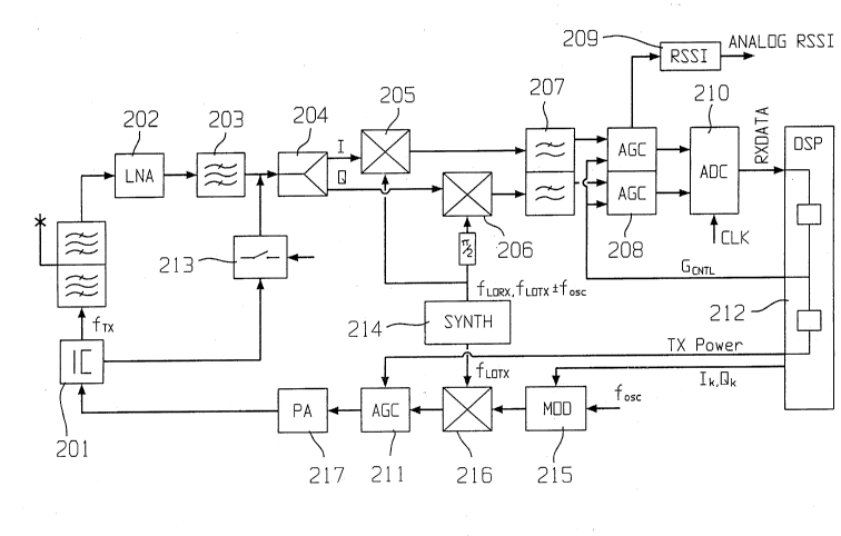
Figure 2 shows a regulating loop according to the present
invention, in which power and distortion are detected in
a direct conversion receiver.
~, -
The prior art according to figure 1 is explained earlier
in the-present application. The radio device based on
direct conversion reception shown in figure 2 is used as
an application example for simplicity. The radio device
of this example operates in both analog and digital
operating modes. The modulating method used in the
digital operating mode is /4-DQPSK modulation.
Application of the present invention-to the radio device
of the figure does not place limitations on the method of
modulation used.
A transmission signal fTx is detected by inputting a small
part of said signal to the carrier frequency part of the
signal path of a receiver, advantageously to the output
of a bandpass filter 203, by means of a directional
coupler 201. When quadrature detection is used, said
signal is divided into two parts by means of a power -~
divider 204 to mix a sideband containins-I and Q
components to the carrier frequency in mixers 205 and
206. The resulting signal components are low pass
filtered 207 and amplified 208.
RSSI information, which is proportional to the power, is
produced based on the amplification of an amplifier, AGC,
208 and the level of a receiver signal RX DATA, which is
sampled by means of an A/D converter 210. Because the
-- 21S~773
level of the received signal is made constant by means of
said adjustable amplifier 208, in practice a signal
proportional to the power is obtained from a control
signal GCNTL of the amplifier 208, which is adjusted to be
proportional to a reference level. From said thusly
detected signal that is proportional to the power, a
- signal, TX POWER, which controls an adjustable amplifier,
AGC, 211, is produced, e.g., in a signal processing unit,
DSP, 212, of the device. In the analog operating mode a
= 10 signal that is proportional to the power can be obtained
directly from a so-called RSSI circuit 209, which is not
described in more detail herein. The circuit is typically
part of an integrated FM detector component.
15 A circuit that realizes the present invention may
include, in addition to the directional coupler 201, a
switch element 213 that switches part of the transmission
signal fTx to the receiver only when the output power is
being detected. The switch element 213 may be an
20 adjustable attenuator, for example. The power divider can
also be implemented capacitively, e.g., by means of a
capacitor. The switch element is not mandatory in a time-
division based digital operating mode, because the
transmitter usually is not in operation during the
25 reception time period and mixing of transmission and
reception signals is not even theoretically possible. In
~-- the analog operating mode, where transmission and
reception occur simultaneously, signal leakage from the
transmitter through the directional coupler 201 in the
direct conversion receiver of figure 2 does not
noticeably disturb normal reception, because the
transmission signal fTx does not mix to the carrier
frequency with the local frequency fLoRx of the receiver,
and the transmission signal fTx and its mixing results
35 with the reception signal are filtered out before signal
detection. Therefore, the switch element 213 is not
2158773
mandatory for the sake of spurious response in the analog
operating mode, either. If the reception signal is mixed
to the intermediate frequency, as is the case in a
conventional heterodyne receiver, the transmission
frequency fTx may, depending on the selected intermediate
frequency, become mixed to the frequency being detected,
resulting in residual modulation. In such a case, the
power sample signal should be attenuated with an
attenuator, which may also include the switch function
21-3.
As a prerequisite for transmission power detection by
means of a direct conversion receiver according to figure
2, in both operating modes the local frequency fLoRx must
be changed to a frequency fLoTx +(~) fosc for the duration
of.the signal detection. This must be taken into account
in the design of the frequency synthesizer, SYNTH, 214.
Implementation of the direct conversion receiver in the
embodiment according to the present invention is
especially advantageous, because in said embodiment fLoTx =
fLoRx whereupon fTx already equals fLoRx + fosc- An
implementation of a synthesizer is described in FI patent
application 945343 filed at the same time as the present
application by the present applicant.
Predistortion that utilizes the circuit according to the
pr~sent invention differs in only two ways from the power
regulating loop described above: firstly, the signal that ~-
is proportional to the distortion can only be separated
after sampling of the demodulized signal with the A/D
converter 210, and secondly, regulation is mainly
directed to the modulation coefficients IK' QKI which are
input to the modulator 215 of the transmitter. The
modulator also may be located in the carrier frequency
part of the transmitter, differing from the example shown
in the figure. Predistortion according to the present
- 215~773
invention is especially advantageous in dual-mode systems
that realize both analog and digital operating modes, in
which there are no obstacles in the analog operating mode
to using an inexpensive, non-linear power amplifier.
Predistortion according to the present invention
implemented in a digital telephone reduces current
consumption.
In principle, predistortion information can also be input
to an ad]ustable amplifier/attenuator, AGC, 211 of the
transmitter.
Power regulation and linearization according to the
present invention occur during the transmission time
period in a system based on time-division. In frequency-
division or code-division systems based on continuous
transmission or reception, detection can be performed at
suitable times, such as during pauses in talking,
whereupon no appreciable noise will enter the reception
signal. The audio output of the receiver can be muted
during detection of the transmission signal. The
estimated time required for detection is typically
approximately lOO~s, which is only a fraction of the
pause occurring in the reception signal during handover,
when one base station is changed to another.
Simple regul-ation of transmission power and linearization
- of the transmission signal can be realized by means of
the present invention without a separate power regulating
or predistortion loop and related components. Power
regulation and linearization can be realized
simultaneously or independently. The dynamics of the
receiver are sufficient for accurate detection of both a
signal proportional to power and a signal proportional to
distortion. Additionally, the sensitivity of the receiver
is much greater than that of a diode detector, whereby
- 2158773
the power sample can be smaller, resulting in minimal
loss in transmission power. In its simplest form, the
circuit according to the present invention is made up of
only a power divider situated in the transmission power
line, one output of which is input to the signal path of
the receiver.
,
Regulation of transmission power to correspond to a given
reference value is carried out digitally in the signal
processing unit of the device, so the slowness caused by
the analog comparator in a regulating loop of the prior
art is eliminated with the present invention.
The benefits of the present invention compared to
embodiments of the prior art are evident in the accuracy,
speed, manufa-cturing costs, current consumption and space
requirements of the regulation. These items are of
particular importance in the strongly competitive hand- -
held telephone market.
In principle, the present invention can be applied in all
radio systems implementing known channelling methods,
TDD, FDD and CDMA. Neither does the modulating method
limit application of the present invention. However, the
present invention is most advantageous in time-division
systems. Predistortion according to the present invention
-- is advantageous in systems in which-non-linear power
amplification can not be implemented without linearizing
procedures that amplify the transmission signal, due to
the modulation method used in said systems, which is
based, at least partly, on amplitude modulation, such as
differential /4-DQPSK, GMSK and QAM. Dual-mode systems,
such as North America's USDMR system, are one
application. The present invention is not limited to the
above examples, but rather can be applied to the extent
permitted by the enclosed claims.