Note: Descriptions are shown in the official language in which they were submitted.
21S877~i
-- 1 --
SINGLE-POLYSILICON CMOS ACTIVE PIXEL
Field of the Invention
This invention relates generally to CMOS active pixels,
and more particularly to a single polysilicon active pixel.
Backgro~nd of the Invention
A CMOS active pixel is a semiconductor device capable
of converting optical images into electronic signals. Such
active pixels may be used in imaging devices such as video
cameras. The CMOS active pixel comprises a photo site and
associated read-out and resetting electronics. As photons
strike a photo site, free charge carriers are generated in
an amount linearly proportional to the incident photon
radiation. These photogenerated charge carriers are
collected in the photo site via a photo gate. The collected
charge carriers form an electrical charge packet. The amount
of charge contained in the charge packet is thus a
representation of the intensity of the light striking the
photo site.
The charge packet is stored in the photo site in
spatially defined depletion regions or potential wells in
the semiconductor substrate beneath the photo site. The
charge packet must be moved from the depletion region under
the photo site to the output circuitry for processing. This
move may be accomplished by transferring the charge packet
to a second, adjacent well that is located beneath a
transfer gate. The transfer gate well receives the charge
from the photo gate well and further transfers it to the
output circuitry for processing.
Charge packet transfer between wells typically occurs
215877~
-- 2
in the following manner. The near-surface potential within
the semiconductor can be controlled by the potential of an
electrode that is in close proximity to the semiconductor
surface. If closely spaced electrodes are at different
voltages, they will form potential wells of different
depths. Free positive charges, for example, holes, will
move from the region of higher potential to the one of lower
potential. Free negative charges, for example, electrons,
will move from the region of lower potential to one of
higher potential. Accordingly, the potential on the photo
gate and transfer gate may be adjusted to effect charge
movement.
There is necessarily a gap between the photo gate and
the transfer gate. If the gap is not narrow enough, the
surface potential under the gap will constitute an
electrical potential barrier for the transfer of the charge
packet. If this occurs, there is no charge transfer. In
other words, there is no signal read-out. Photolithographic
techniques presently dictate that a two layer polysilicon
structure is required to achieve a sufficiently narrow gap
between surface electrodes.
It would be desirable to form an active pixel using a
process wherein only one polysilicon deposition is required.
This simple process would result in lower per chip
fabrication cost. Furthermore, it would be desirable to
operate such a pixel in a manner that minimizes hardware
requirements while maintaining optimal pixel performance.
SummarY of the Invention
A single-polysilicon active pixel formed based on a
single polysilicon deposition, and a method for operating
the single-polysilicon active pixel are disclosed.
According to one aspect of the present invention, the
single-polysilicon active pixel comprises a photo site, a
photo gate, a transfer transistor, and output and reset
21~877S
-- 3
electronics. The source of the transfer transistor may be
a doped region of substrate, referred to as a coupling
diffusion, which provides the electrical coupling between
the photo gate and the transfer transistor. The coupling
diffusion allows for the transfer of a signal stored in the
photo site under the photo gate to the output electronics
for processing.
According to another aspect the invention, the single-
polysilicon active pixel may be operated by biasing the
transfer transistor to the low operating voltage of the
pixel, for example, 0 volts. By virtue of the structure of
the single-polysilicon active pixel, this mode of operation
results in the same timing as if the transfer transistor
were clocked, which it is not, so that neither a clock nor
the associated driving circuitry are required. However,
there is little or no tendency for image lag as occurs in
double polysilicon active pixels when they are operated in
a manner which avoids clocking the transfer gate.
Further features of the present invention will become
more apparent from the following detailed description when
read in conjunction with the accompanying drawings.
Brief DescriDtion of the Drawinqs
FIG. 1 is a prior art double polysilicon active pixel;
FIG. 2 provides detail as to the prior art two-layer
structure of the active pixel of FIG. l;
FIG. 3 is a schematic of a single-polysilicon active
pixel according to the present invention; and
FIG. 4 is a flow chart illustrating a method of
operating the single-polysilicon active pixel of FIG. 3
according to the present invention.
21S8~7S
-- 4
Detailed Descri~tion of the Invention
Before discussing the single-polysilicon CMOS active
pixel 36 of the present invention which is shown in FIG. 3
and described in conjunction with a discussion of FIGS. 3
and 4 below, it will be useful to discuss the structure and
operation of a typical double-polysilicon active pixel.
A schematic and electron transfer diagram of a prior
art double-polysilicon CMOS active pixel 35 is shown in FIG.
1. FIG. 1 does not, however, illustrate the double
polysilicon layer. Details of the double polysilicon layer
are shown in FIG. 2.
Referring to FIG. 1, the active pixel 35 may be
represented as a photo gate 101 charge-coupled to a transfer
gate 107 that is charge-coupled to a diffusion region 110.
The active pixel 35 further includes a reset transistor 120,
a voltage-follower transistor 125, and a select transistor
130. A load, such as a suitably biased load transistor 135
may be included as part of the pixel. Typically, the active
pixel 35 will be one of a plurality of such active pixels
forming an array. As such, is it preferable to use a single
load transistor 135 that is common to a column of active
pixels, the column containing other active pixels such as
the pixels 37 and 38, for example. While two additional
pixels 37 and 38 are shown, it will be understood that many
more pixels might be included depending upon the application
of the invention.
A floating diffusion node 115 connects the diffusion
region 110 to the reset transistor 120 and the voltage-
follower transistor 125. The reset and voltage-follower
transistors are further connected to a fixed voltage VDD
which may be, for example, five volts. The reset transistor
120 is also connected to a reset control line 184 from an
external signal timing controller 190. The voltage-follower
- 215877~
-- 5
transistor 125 is further connected to the select transistor
130 which is electrically connected to the load transistor
135.
The load transistor 135 is also connected to a fixed
load voltage VLOAD, and a fixed voltage VSS which may be,
for example, zero volts. The select transistor 130 is
further connected to a select control line 186 from the
signal timing controller 190. The signal timing controller
may be a timing circuit, a combinational logic circuit or
any other circuit capable of generating the necessary timing
signals to the active pixel. The load voltage VLOAD should
be adjusted such that a desired resistance is achieved
across the load transistor 135 between the node 50 and the
fixed voltage VSS. Accordingly, suitable alternatives for
the load transistor 135 include a resistor or any other
passive or active device that can provide the required
electrical resistance when disposed between the node 50 and
the fixed voltage VSS.
The active pixel output 50 that generates the output
signal is the connection point between the select transistor
130 and load 135. The pixel output line 65 connects the
pixel output 50 to an output circuit, such as the
differential output circuit described in U.S. Patent
application S.N. 08/323203 filed on October 14, 1994 and
incorporated herein by reference.
FIG. 1 includes an electron well diagram showing charge
carriers 102 beneath the photo gate 101, charge carrier
transfer arrow 106 and transferred charge carriers 111 in
the diffusion region 110. This diagram represents the
transfer of electrical charge from the region under the
photo gate 101, which may be referred to as a photo site, to
the transfer channel under the transfer gate 107 to the
diffusion region 110. The transfer of charge will be
discussed in more detail below.
The double-polysilicon structure, illustrated in FIG.
2~877S
2, provides the electrical coupling required for
transferring charge from the semiconductor substrate region
103 under the photo gate 101 and to the region 104 under the
transfer gate 107. The substrate surface potential under
the photo gate 101 is controlled by the voltage applied to
the photo gate 101. Similarly, the substrate surface
potential under the transfer gate 107 is controlled by the
voltage applied to the transfer gate 107. Charge transfer
from the region 103 to the region 104 and finally to the
diffusion region 110 is achieved by applying a different
voltage to the photo gate 101 and the transfer gate 107. If
the gap 12 between the photo gate 101 and the transfer gate
107 is not narrow enough, the substrate potential under the
gap 12 will constitute a barrier for the transfer of the
charge.
To form the double polysilicon arrangement, a first
layer of polysilicon is deposited on the substrate. The
polysilicon is then patterned, and a contact is attached.
The patterned polysilicon and contact collectively form the
photo gate 101. A thin layer of an insulating material,
typically silicon dioxide, is then grown. Next, a second
layer of polysilicon is deposited. The second deposition is
then patterned and a contact is attached. The patterned
second deposition and the contact collectively form the
transfer gate 107. The transfer gate 107 may overlap the
photo gate 101. As shown in FIG. 2, the gap 12 separating
the photo gate 101 and the transfer gate 107 is as narrow as
the thickness of the silicon dioxide layer 109, which is
typically on the order of a few tens of nanometers (nm).
This narrow gap is essential for proper electrical coupling.
The active pixel may be either an n-channel device with
electrons as the photo-generated charge carriers or a p-
channel device with holes as the photo-generated charge
carriers. For the balance of this description, the active
pixel is assumed to be an n-channel device.
21~ ~ ~ 7 ~
-- 7
The signal timing controller 190 generates reset,
select and photo gate control signals on lines 184, 186 and
180 causing the double-polysilicon active pixel to operate
in two phases, integration and read-out. In the integration
phase, the generated charge carriers are collected under the
photo gate 101 for a predetermined period, referred to as
the integration time. The integration time is dictated by
the frame rate, or in other words, the number of times per
second an image is updated, of the particular imaging
application for which the active pixel is being used. For
example, for commercial video applications, the frame rate
is 30 frames per second. Thus, the integration time is
about 1/30 of a second. The charge carriers are collected
by clocking the photo gate 101 to a relatively high voltage
level, such as VDD. During the integration phase, the
transfer gate 107 is turned off. In the read-out phase,
the reset transistor 120 is pulsed on and off. This pulsing
causes the potential of the diffusion node 115 to float at
a level approximately equal to VDD less the threshold
voltage. Then, the bias of the photo gate 101 is changed to
approximately VSS, for example, 0 volts, causing charge
transfer to the diffusion node 115. Charge transfer causes
the potential of the diffusion node 115 to deviate from its
value, approximately VDD, or in other words, the reset
level, to another value which is dictated by the photo-
generated charge. This other value is the signal level.
The difference between the reset and signal levels is
proportional to the incident light intensity and constitutes
a video signal. A source follower comprising the voltage-
follower transistor 125 and a load transistor 135 is used tobuffer the diffusion node 115 from the output 50 of the
active pixel sensor 35.
The select transistor 130 is used to select the pixel
for read-out. In this phase, the transfer gate 107 is
turned on to allow the transfer of the signal charge from
~158775
-
-- 8
under the photo gate 101 into the diffusion node 115. It is
turned off, however, after completion of transfer and before
the photo gate is clocked high for the following
integration, ensuring that none of the signal charge will
transfer back to the region under the photo gate 101 causing
image lag.
The transfer gate 107 should be clocked on and off as
described above for the optimum operation of the pixel.
Alternatively, it is known to operate the pixel by biasing
the transfer gate 107 to a voltage approximately halfway
between VSS and VDD, or in other words, about 2 to 2.5 volts
for a typical application so that the transfer channel is
slightly conducting. This biasing simplifies operation by
eliminating the need for one control clock and the
associated driving circuitry. But, some of the charge
signal may transfer back to under the photo gate 101
resulting in image lag, especially at high charge signal
levels.
After the charge signal read-out, the output 50 signal
is processed and amplified to provide the output video
signal.
As previously noted, it is desirable to fabricate a
CMOS active pixel based on a single polysilicon deposition.
If, however, the photo gate 101 and the transfer gate 107
are formed in this manner, the gap between the photo gate
and the transfer gate would be approximately one micron
(~m). A one micron gap is too wide to provide the required
electrical coupling. In one embodiment of the present
invention, a CMOS active pixel that is based on a single
polysilicon deposition is described.
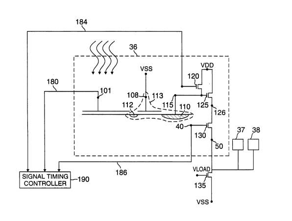
One such single-polysilicon CMOS active pixel 36
according to the present invention is shown in FIG. 3. The
elements of the single-polysilicon active pixel are similar
to those of the double-polysilicon active pixel. Unlike the
double-polysilicon active pixel, however, the single-
215~77~
-
g
polysilicon active pixel 36 has a coupling diffusion region
112 situated between the photo gate and the transfer gate.
The coupling diffusion region 112, the diffusion region 110
and the transfer gate function collectively as a transistor,
the coupling diffusion region as the source, and the
diffusion region 110 as the drain. Thus, a transfer
transistor 113 is formed comprising the coupling diffusion
region 112, a diffusion region 110, and a transfer
transistor gate 108. When properly biased as discussed
further below, the coupling diffusion region functions as a
conduction channel between the substrate regions 103 and
104, thus providing the required electrical coupling.
To form the photo gate 101 and the transfer transistor
gate 108, a layer of polysilicon is deposited on a
semiconductor substrate. The polysilicon is then patterned
into two regions, using an appropriate mask, defining the
photo gate 101 and the transfer transistor gate 108. Such
a masking technique is well known to those skilled in the
art. The coupling diffusion region 112 and the diffusion
region 110 may suitably be formed in the same ways that the
source and drain regions of a transistor are typically
formed.
The coupling diffusion region 112 increases the kTC
noise of the pixel. This effect can be minimized by making
the coupling diffusion region capacitance as low as possible
by making the area of the coupling diffusion region 112 as
small as possible. It is expected that the coupling
diffusion region capacitance can be made as low as a few
femto-Farads, which equates to kTC noise on the order of a
few tens of electrons.
The single-polysilicon CMOS active pixel 36 can be
operated in a manner similar to that of the double-
polysilicon CMOS active pixel. For example, the transfer
transistor 113 may be turned on and off in a manner similar
to that of the transfer gate 107. Alternatively, the
2158775
- 10 -
transfer transistor may be biased with a potential
approximately halfway between VSS and VDD so that it is
slightly conducting. As in the case of the double-
polysilicon active pixel, the latter operating mode results
in a trade-off between operating simplicity and image lag.
In considering the single-polysilicon CMOS active pixel
36, a novel mode of operation has been discovered. As shown
in FIG. 4 and described below, a presently preferred method
of operation is as follows. In step 200, the transfer
transistor gate 108 is biased to VSS, typically O volts. In
step 210, the photo gate 101 is clocked high by applying a
voltage such as 5 volts, and the photo-generated electrons
are collected. During collection, the transfer transistor
113 is off. This is because the gate-to-source voltage is
zero, and thus lower than the threshold voltage. In step
220, which occurs near the end of the integration time, the
potential on the diffusion region 110 is reset. This
resetting may be accomplished in the same manner as for the
double-polysilicon pixel. For example, a reset transistor
120 may be pulsed on and off, causing the potential of the
diffusion node 115 to float at a level approximately equal
to VDD less the threshold voltage. Finally, in step 230,
the photo gate 101 is clocked low by applying a voltage such
as 0 volts, so that the electrons are transferred out of the
region under the photo gate 101.
Without being limited to a particular theory of
operation, it is believed that the pixel operates as follows
when the transfer transistor gate is biased to VSS. Once
the photo gate 101 is clocked low, the potential of the
coupling diffusion region 112 goes slightly negative as it
gets flooded by the electrons as they flow from the region
under the photo gate 101. As the coupling diffusion region
112 potential decreases or becomes negative, the gate-to-
source voltage of the transfer transistor 113 increases or
becomes positive. Concurrently, because of the body effect,
215 ~ ~ 7 ~
the threshold voltage of the transfer transistor 113
decreases. This mechanism remains in effect until the gate-
to-source voltage exceeds the threshold voltage causing the
transfer transistor 113 to turn on. As the transfer
transistor turns on, the electrons flow from the coupling
diffusion region 112 to the diffusion node 115. The flow of
the electrons continues until the potential of the coupling
diffusion region 112 decreases to its previous level, that
is, its potential before the transfer of the signal
electrons from the region under the photo gate 101, causing
the transfer transistor 113 to turn off. The pixel is then
ready to process another image by repeating the
aforementioned steps as indicated by line 240.
Biasing the transfer transistor gate 108 to VSS causes
the transfer transistor 113 to be off all the time except
when the electrons are transferred from under the photo gate
101 into the diffusion node 115. This is effectively the
same timing as if the transfer transistor 113 were clocked.
Neither a clock nor its associated driving circuitry is
required, however. Further, because the transfer transistor
gate 108 is biased to VSS, i.e., nominally zero volts, there
is no tendency to lag as when the transfer gate is biased to
a voltage intermediate between VDD and VSS.
This mode of operation, which may be referred to as
virtual clocking of the transfer transistor, is less
sensitive to very low signal levels, for example, less than
about one-half of one percent of the signal saturation
level. If the signal level is in this range, the potential
of the coupling diffusion region 112 will not become
negative enough to cause the transfer transistor 113 to turn
on. To this end, the capacitance of the coupling diffusion
region 112 must therefore be made as low as possible.
Note that the potential of the coupling diffusion
region 112 does not get sufficiently negative to cause the
coupling diffusion/substrate junction to be forward biased.
215877S
- 12 -
The transfer transistor 113 turns on before the coupling
diffusion-substrate junction potential exceeds its built-in
value, causing this junction to remain reverse-biased as the
transfer transistor turns on and then off.
The single-polysilicon CMOS active pixel 36 of the
present invention may be comprised of the same elements that
are used in a double polysilicon active pixel for providing
read-out, reset and buffering functions. For example, the
single-polysilicon CMOS active pixel may incorporate a reset
transistor 120, a voltage-follower transistor 125, select
transistor 130 and a load, such as a suitably biased load
transistor 135. Alternatively, the load transistor need not
be included in the pixel 36 but may be common to a column of
such pixels. These elements are arranged to operate in a
manner similar to their operation in the double-polysilicon
active pixel. The photo gate 101, the reset transistor 120
and the select transistor 130 are controlled, as
appropriate, by a signal from the signal timing controller
190 sent over lines 180, 184 and 186, respectively.
A plurality of single polysilicon active pixels 36
according to the present invention may be arranged to form
an imaging array which may be used as a solid-state camera.
In an exemplary imaging array, one or more signal timing
controllers may be employed to sequentially activate the
pixels in each row generating a serial video signal
corresponding to an image focused on the array.