Note: Descriptions are shown in the official language in which they were submitted.
. - .
PD-N94094
METHOD AND DEVICE FOR CANCELLING RECEIVED FREQUENCY OFFSET
BACKGROUND OF THE INVENTION
Hybrid-earth-station (HES) systems include receivers
capable of receiving and demodulating satellite signals
modulated with both voice and data information.
Typically, an HES receiving site includes a satellite
dish coupled to several signal downconverter stages. The
satellite dish is oriented toward the path of the
satellite and receives a broadband transmission of Ku-
band signals containing voice and data information. A
downconverter stage on the satellite dish shifts the Ku
band signals down to L-band. The L-band signals are then
transmitted along a cable to an L-band radio where
another downconverter stage further shifts the frequency
of the signals and retrieves the information carried on
the signals.
In each instance of shifting, the incoming signals
are shifted from one predetermined frequency bandwidth to
' another . One or more carrier f requencies , each modulated
to carry voice or data information, may exist in the
shifted bandwidth. Demodulators in the L-band radio each
look for a particular carrier frequency in the shifted
bandwidth to demodulate.
The downconverters often shift a band of frequencies
more or less than desired. Such shifting inaccuracies
can be caused by temperature changes in the oscillators
located in the downconverters. Inaccurate shifting
results in the signals arriving at the demodulators
offset from the expected frequencies.
Voice information is particularly sensitive to any
~ frequency offsets that originate in the HES receiver or
at any other point prior to retrieving the information
from the signal. Previously, receivers attempted to
combat frequency offsets by using very accurate, but
- 1 -
. ,.'. .
- 2 -
expensive, oscillators and frequency reference devices to
ensure accurate frequency shifting.
Another approach to combatting frequency offsets is
to use demodulators that have broad searching and
tracking capability to individually search the frequency
band for the particular carrier the demodulator has been
assigned. However, the typical demodulator can only
sweep small segments of a frequency spectrum at one time.
After sweeping each small segment, the demodulator must
jump to the next segment and again sweep for its assigned
carrier frequency. An audible "click~~ occurs on a
telephone communication line each time the demodulator
jumps to another segment.
Accordingly, there is a need for an accurate
receiver that is inexpensive and can adequately
compensate for the frequency offsets that can occur in
voice communications.
SUMMARY OF THE INVENTION
The present invention relates to a method and device
for canceling frequency offsets in received modulated
signals. The present invention provides a frequency
tracking feedback loop having receiver circuitry that is
inexpensive yet accurate enough for voice information
demodulation, such as in telephone communications, all
without compromising performance.
The device includes a downconverter module that
receives the modulated signals in a predetermined
frequency range and shifts the received signals to a
lower frequency band centered at a first intermediate
frequency (IF). A channel unit,receives the first IF,
shifts it to a second IF, demodulates at least one
information signal from the band of signals centered at
the second IF, and generates a frequency offset output.
The frequency offset output is then used supply any
needed adjustments to the aforementioned frequency
- 2 -
CA 02158880 1999-11-09
- 3 -
shifts, thereby compensating for any detected frequency offset.
The method of the present invention includes the steps of
receiving the modulated signals in a predetermined frequency range
and shifting them to an IF. The expected signal is searched for in
the IF, and any frequency offsets are calculated from that expected
frequency. The frequency offset information is translated into
offset correction data, and the offset correction data is fed back
to correct for the detected error. The modulated signals are then
continuously tracked after acquiring them.
Aspects of the present invention are as follows:
A device for canceling frequency offsets in received modulated
signals, the device comprising:
a downconverte:r module receiving the modulated signals in a
predetermined frequency range, and shifting the modulated signals
to a first IF; and
a channel unit receiving the first IF, and generating a
frequency offset output coupled to the downconverter for adjusting
the downconverter to compensate for any frequency offset.
A method of canceling frequency offset in received modulated
signals, the steps comprising:
receiving the modulated signals in a predetermined frequency
range;
shifting the modulated signals to an IF;
detecting a frequency offset in a channel decoder;
calculating the amount of frequency offset;
feeding back frequency offset correction output.
The invention itself, together with further objects and
attendant advantages, will be best understood by reference to the
following detailed description, taken in conjunction with the
accompanying drawings.
11-30-99 03:47pm From-SIM ~BURNEY 4165951163 T-151 P.02/02 F-968
- 3a -
88I8F DESCAIBTION OF THE DRAWINGS
Figure 1 is a diagram of a satellite dish and a hybrid earth
station receiver.
Figure 2 is a block diagram o a satellite dish and a hybrid
earth station receiver.
Figure 3 is a block diagram i3lustrating in more detail the
downconverter module, channel until, and control module shown in
Figure 2.
Figure ~ is a block diagram of the mixing stage used in the
downconverter shown in Figure 3.
Figure 5 is a flowchart showing the steps of a searching and
tracking computer
program that
may be used
to compensate
for the
detected frequency
offset.
DETAILED DESCAIFTION OF THE DRAWINGS
Figure 1 ig a block diagram of a satellite receiver chain l0
embodying the present inverition. The satellite receiver chain 10
has a satellite
antenna 12
coupled to
a Ku-bank
block downconverter
lg mounted the antenna 12. The antenna 12 may be a satellite
on
~ ~'~~r ~~rm -..
CA 02158880 1999-11-09
- 4 -
of antenna appropriate for receiving Ku-band signals.
The block downconverter 14 receives Ku-band signals from
the antenna 12, shifts them down to L-band, and transmits
the L-band signals through a cable 16 to the hybrid-
s earth-station (HES) receiver 18. The HES receiver 18
(shown in greater detail in Figures 2 and 3) splits the
input signals into two paths, each carrying the identical
L-band signals. One path is directed to a personal-
earth-station (PES) receiver section 19, and the other
path is directed to a telephony-earth-station (TES)
receiver section 17. Both receiver sections 17, 19 shift
the L-band signals to an even lower frequency band so
that demodulators in the receiver sections 17, 19 can
remove information from the received modulated signals.
In addition, the receiver 18 detects and compensates for
any signal offset in the received modulated signals
regardless of whether the offset originated in doppler
errors, errors in the block downconverter 14 or the
receiver 18 itself. The HES receiver 18 outputs
information signals along cables 20 to the proper voice
or data receiving destinations 22, 24.
The present invention relates primarily to the TES
receiver section 17 of the HES receiver 18. More
particularly, the invention relates to the TES receiver
section's 17 ability to detect and cancel frequency
offsets introduced into the received modulated signals.
By compensating for frequency offset in the manner
disclosed herein, the TES receiver section 17 and the
block downconverter 14 can be constructed of less
expensive components. The PES receiver section 19 does
not need the frequency offset cancellation hardware and
software of the present invention because PES technology _.
involves mainly data communications that are less
sensitive to frequency offsets.
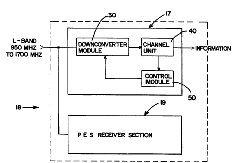
Figure 2 is a block diagram of a preferred TES
receiver section 17 embodying the.present invention. The
- 4 -
.. . 21~88gU
- 5 -
TES receiver section 17 includes a downconverter module
30, a channel unit 40, and a control module 50.
Preferably, the downconverter module 30 is constructed on
a portion of a larger circuit board occupied by the
control module circuitry 50.
The downconverter module 30 receives the modulated
L-band signals from the block downconverter 14 (shown in
Figure 1) . The incoming L-band signals are preferably in
the range from approximately 950 MHz to approximately
1700 MHz. The downconverter module 30 shifts a portion
of the L-band signal to a first intermediate frequency
(IF). Preferably, the first IF is centered at
approximately 70 MHz and the shifted portion of the L-
band signal is approximately 40 MHz wide. The
downconverter 30 also receives a frequency correction
output in a feedback loop from the control module 50.
The downconverter 30 uses the frequency correction output
to adjust for frequency offset detected in the channel
unit 40 and translated in the control module 50.
The channel unit 40 receives the first IF and
searches for predetermined carrier frequencies. The
channel unit 40 accomplishes the search by shifting the
first IF to a second, lower, IF and then sweeping the
bandwidth around the second IF looking for signals to
demodulate. The channel unit 40 demodulates the signals,
generating both information signals and freauency offset
outputs for use in adjusting the downconverter module 30
to compensate for any frequency offset that may exist.
The control module 50 receives the frequency offset
output from the channel unit 40 and translates the
frequency offset output into frequency correction output
to be fed back to the downconverter module 30. In a _
preferred embodiment the frequency correction output is
a digital signal. The control module 50 translates the
frequency offset information by averaging the frequency
offset information and computing the direct_on and speed
- 5 -
2~ ~~~8~
- 6 -
that the downconverter module 30 must shift the first IF.
The control module 50 limits the rate of frequency change
such that the channel unit 40 can properly track the
signal as it moves. In a preferred embodiment the
control unit can instruct the downconverter module 30 to
shift the first IF as much as +/- 300 kHz in
approximately 10 Hz increments.
Figure 3 is a more detailed illustration of the
downconverter module 30, channel unit 40 and control
module 50 shown in Figure 2. In a preferred embodiment,
the downconverter module 30 includes a radio frequency
(RF) amplifier stage 31, a first mixing stage 32, a band
pass filter 33, an IF amplifier 34, a second mixing stage
35, a low pass filter 36, an output amplifier 37, and a
digital to analog (D/A) converter 38. The RF amplifier
stage 31 receives the modulated signals and amplifies the
L-band signal level prior to the first mixing stage 32.
The RF amplifier stage 31 is preferably an automatic gain
control stage that amplifies the signals to a
predetermined level. The first mixing stage 32 is
coupled to the RF amplifier 31 and shifts the L-band down
in frequency. The band pass filter 33 filters off the
undesired harmonics and noise leaving the desired
bandwidth of signals. The filtered signals are next
amplified in an IF amplifier 34, preferably an automatic
gain control circuit such as a Siemens BAR61, and shifted
to the desired first IF in the second mixing stage 35.
The shifted signals, now preferably a first IF centered
at approximately 70 MHz, are filtered in a low pass
filter 36. After passing through the low pass filter 36,
the first IF is amplified in an output amplifier 37 and
leaves the downconverter module 30. The output amplifier
37, in a preferred embodiment, is an Avantek INA 02186
amplifier.
The D/A converter 38,is preferably coupled to the
first mixing stage 32. The D/A converter 38, such as an
- 6 -
~~~~~g0
,:~
_ 7 _
Analog Devices AD1851, translates the digital correction
output from the control module 50 into a tuning voltage
for tuning the first mixing stage 32 and shifting the IF
to correct for detected offset. In another preferred
embodiment, the D/A converter 38 is coupled to the second
mixing stage 35 for tuning the IF with the second mixing
stage 35 rather than the first mixing stage 32.
The first and second mixing stages 32, 35 are shown
in more detail in Figure 4. The first and second mixing
stages 32, 35 each include a frequency synthesizer 60 and
a mixer 62. The frequency synthesizer 60 generates a
local oscillator (LO) frequency for mixing with the
modulated signals fed to the mixer 62. The mixer 62
mixes the LO and the modulated signals to shift the
modulated signals down in frequency. Each of the mixing
stages 32, 35 generates a different LO frequency such
that the L-band signals are shifted down to an IF,
preferably centered at approximately 70 N~iz, after
passing through both mixing stages 32, 35. The mixer 62
in the first mixing stage 32 may be a Synergy SNDC3
mixer. The mixer 62 in the second mixing stage 35 may be
a Siemens PMB2306 mixer.
The synthesizer 60 in each mixing stage 32, 35 is
preferably a phase-lock-loop (PLL) technology tunable
synthesizer but may be any synthesizer capable of fine
frequency tuning. A presently preferred embodiment
includes a voltage controlled crystal oscillator (VCXO)
in the first mixing stage 32 to receive the tuning
voltage from the D/A converter 38. The tuning voltage
tunes the synthesizer 60 in the first mixing stage 32,
which causes the modulated signals to be shifted by an
amount that compensates for the offset detected in the
channel unit 40. The second mixing stage 35, rather than
the first mixing stage 32, may receive the frequency
correction tuning voltage in another preferred
embodiment.
_ 7 _
~~ ~~~so
_s-
In yet another preferred embodiment, the
downconverter module 30 does not have a D/A converter 38
and the digital frequency correction output of the
control unit 50 connects directly to the synthesizer 60
of either the first or second mixing stages 32, 35. The
synthesizer 60 receives the frequency cancellation
feedback directly from the control module 50.
Preferably, the synthesizer 60 is a direct digital
synthesizer capable of fine frequency tuning.
Returning now to Figure 3, a first IF signal is fed
from the output amplifier 37 to the channel unit 40.
Preferably, the channel unit 40 has at least one channel
decoder 45. The channel unit 40 may have telephony-
earth-station (TES) channel decoders for primarily voice
communication, personal-earth-station (PES) decoders for
primarily data communications, or a mixture of both. By
definition, a hybrid-earth-station (HES) receiver 18 is
designed to handle both TES and PES signals. While PES
technology does not need the same frequency offset
cancellation as TES, a single downconverter module 30, as
in the present invention, may be used for both.
Preferably, the channel unit 40 contains one or more
channel decoders 45 of the TES type. In another
preferred embodiment, both TES and PES channel decoders
45 may be used in the TES receiver section 17 (Figure 1).
Each channel decoder 45 contains a downconverter 42
for shifting the first IF to a frequency that can be
demodulated, a demodulator 43, and a channel decoder
microprocessor 44. Each channel decoder downconverter 42
receives the first IF and shifts the first IF to a second
IF. A NEC UPC1686 is suitable for use as the
downconverter 42.
The demodulator 43 is connected to the downconverter
42. The demodulator 43 receives the second IF and
retrieves information from the particular carrier
frequency that the particular channel decoder 45 is
- 8 -
2~~88g0
_ 9. _
assigned to. The demodulator 43, in addition to
producing an information signal, produces frequency
offset data. The demodulator 43 preferably sends offset
data, representative of the offset it detected, in 1 Hz
increments. A Texas Instruments TMS320C is suitable for
use as the demodulator 43. The channel decoder
microprocessor 44, which may be implemented as an Intel
80C188, receives the offset data and feeds back a
frequency offset output to the downconverter 42 in the
channel unit 40. The frequency offset output causes the
decoder downconverter 42 to sweep for its preassigned
carrier frequency when it is initially acquiring the
carrier frequency or when the carrier frequency shifts
more than a threshold amount. Additionally, each channel
decoder microprocessor 44 transmits a frequency offset
output to the control module 50. The frequency offset
output fed back to the control module 50 contains the
total offset measured. Preferably, each microprocessor
44 transmits information indicating whether or not the
signal has been found and what the offset is in 10 Hz
increments. Frequency offset.may be determined by any
suitable method such that a frequency offset output,
translatable by a microprocessor, is generated. A
preferred method of determining frequency offset is
described later in this disclosure.
The frequency offset output data transmitted to the
control module 50 arrives first at a serial link 51 and
is forwarded to the control module microprocessor 52. In
a preferred embodiment, the microprocessor 52 averages
the offset information from each channel decoder 45 and
controls the rate that downconverter module 30 is sent
frequency offset corrections. The control module
microprocessor 52, preferably a Siemens SOC535, sends a
frequency offset cancellation output through a shift
register 53 to the D/A converter 38 on the downconverter
module 30. In a preferred embodiment, the frequency
g _
.. 2.~ ~5~~0
- 10 -
offset cancellation output is a digital signal that is
converted by the D/A converter 38 to an analog voltage.
Figure 5 illustrates the steps that the channel unit
40 makes in searching for, acquiring and then tracking
the desired carrier frequencies. In first searching for
the carrier, each channel decoder 45 in the channel unit
40 tunes its downconverter 42 to find its preassigned
carrier frequency. The channel decoder microprocessor 44
instructs the downconverter 42 to sweep frequency
segments of the second IF until the carrier is found.
Preferably, the frequency segments are approximately 400
Hz. Once the assigned carrier frequency has been found,
the carrier is constantly tracked by the channel decoder
microprocessor 44 using frequency offset data generated
by the demodulator 43.
While the carrier frequency being tracked remains
within a predetermined frequency threshold, the channel
unit 40 transmits the frequency offset output to the
control module 50. Each channel decoder microprocessor
44 calculates frequency offset by adding offset detected
by the demodulator 43 to the frequency offset of the
synthesizer in the channel decoder downconverter 42. The
frequency offset in the channel decoder downconverter 42
is the amount the microprocessor 44 has tuned the
synthesizer in the downconverter 42 from its preset
default frequency. If the frequency being tracked
deviates an amount greater than a preset threshold, both
the synthesizer in the channel decoder downconverter 42
and the downconverter module 30 are tuned to compensate.
In a preferred embodiment, the channel decoder
downconverter 42 is a coarse frequency tuner capable of
tuning in approximately 400 Hz increments. The coarse
tune feedback loop is entirely within the one or more
channel decoders 45 in the channel unit 40.
Specifically, the coarse tune feedback loop includes the
tunable downconverter 42, the demodulator 43, and the
- 10 -
2.~ ~8~~0
- 11 -
channel decoder microprocessor 44 in each channel decoder
45. Once the signal is acquired, fine tuning is
accomplished by the control module 50 which can tune the
downconverter module 30 in 10 Hz increments. The fine
tune feedback loop consists of the downconverter module
30, the channel unit 40, and the control module 50.
A preferred method of canceling received frequency
offset is to calculate the offset by averaging frequency
offset data from all the channel decoders 45. This
method provides a redundancy check benefit in case a
particular channel decoder 45 is providing erroneous
data. Alternatively, a preferred embodiment of the
present invention includes randomly selecting, or
preselecting one channel decoder 45 to provide the
frequency offset data. Because any frequency offset
introduced in the frequency shifting chain from the
antenna 12 should affect all of the carrier frequencies
equally, the error detected for a particular carrier
frequency will be the same for all carrier frequencies.
In summary, the foregoing describes a method and
device for canceling frequency offset in received
modulated signals. The method and device utilize a
feedback loop that finely tunes a single L-band
downconverter in the receiver to correct for any
frequency offset detected in the one or multiple channel
decoders. This provides a simple design that does not
require highly accurate and expensive oscillators.
Additionally, the frequency tracking of the present
method and device is accurate enough for use in TES
communications that are generally sensitive to frequency
offsets.
It is intended that the foregoing detailed
description be regarded as illustrative rather than
limiting, and that it be understood that it is the
following claims, including all equivalents, which are
intended to define the scope of this invention.
- 11 -