Note: Descriptions are shown in the official language in which they were submitted.
215 8 8 X ~ CFO 10059 CA
ELECTRON-EMITTING DEVICE AND METHOD OF MANUFACTURING
THE SAME AS WELL AS ELECTRON SOURCE AND IMAGE FORMING
APPARATUS COMPRISING SUCH ELECTRON-EMITTING DEVICES
BACKGROUND OF THE INVENTION
Field of the Invention
This invention relates to an electron-emitting
device having a novel structure and also to an electron
source and an image forming apparatus comprising such
electron-emitting devices.
Related Backqround Art
There have been known two types of
electron-emitting device; the thermionic cathode device
and the cold cathode device. Cold cathode devices
refer to the field emission type (hereinafter referred
to as the FE type), the metal/insulation layer/metal
type (hereinafter referred to as the MIM type), the
surface conduction type, etc. Examples of FE type
device include those proposed by W. P. Dyke & W. W.
Dolan, "Field emission", Advance in Electron Physics,
8, 89 (1956) and C. A. Spindt, "PHYSICAL Properties of
thin-film field emission cathodes with molybdenum
cones", J. Appl. Phys., 47, 5248 (1976).
Examples of MIM device are disclosed in papers
including C. A. Mead, "Operation of Tunnel-Emission
Devices", J. Appl. Phys., 32, 646 (1961).
Examples of surface conduction electron-emitting
-
- 221~ ~88~
device include one proposed by M. I. Elinson, Radio
Eng. Electron Phys., 10, 1290 (1965).
A surface conduction electron-emitting device is
realized by utilizing the phenomenon that electrons are
emitted out of a small thin film formed on a substrate
when an electric current is forced to flow in parallel
with the film surface. While Elinson proposes the use
of SnO2 thin film for a device of this type, the use of
Au thin film is proposed in [G. Dittmer: "Thin Solid
10Films", 9, 317 (1972)] whereas the use of In203/SnO2 and
that of carbon thin film are disclosed respectively in
[M. Hartwell and C. G. Fonstad: "IEEE Trans. ED Conf.",
519 (1975)] and [H. Araki et al.: "Vacuum", Vol. 26,
No. 1, p. 22 (1983)].
15Fig. 60 of the accompanying drawings schematically
illustrates a typical surface conduction
electron-emitting device proposed by M. Hartwell.~ In
Fig. 60, reference numeral 1 denotes a substrate.
Reference numeral 3 denotes an electroconductive thin
film normally prepared by producing an H-shaped thin
metal oxide film by means of sputtering, part of which
eventually makes an electron-emitting region 2 when it
is subjected to an electrically energizing process
referred to as "energization forming" as will be
described hereinafter. In Fig. 60, a pair of device
electrodes are separated by a length L of 0.5 to l[mm]
and a width W' is O.l[mm].
~ 3 ~ 21a 8~86
Conventionally, an electron emitting region 2 is
produced in a surface conduction electron-emitting
device by subjecting the electroconductive thin film 3
of the device to an electrically energizing process,
which is referred to as energization forming. In the
energization forming process, a DC voltage or a slowly
rising voltage that rises typically at, for instance, a
very slow rate of lV/min. is applied to given opposite
ends of the electroconductive thin film 3 to locally
destroy, deform or structurally modify the film and
produce an electron-emitting region 2 which is
electrically highly resistive. Thus, the
electron-emitting region 2 is part of the
electroconductive thin film 3 that typically contains
fissures therein so that electrons may be emitted from
the fissures and their neighboring areas. Note that,
once subjected to an energization forming process, a
surface conduction electron-emitting device comes to
emit electrons from its electron emitting region 2
whenever an appropriate voltage is applied to the
electroconductive thin film 3 to make an electric
current flow through the device.
In an image display apparatus realized by
arranging a large number of surface conduction
electron-emitting devices of the above described type
on a substrate and an anode electrode disposed above
the substrate, a voltage is applied to the device
- 4 ~ 215 888~
electrodes of selected electron-emitting devices to
cause their electron-emitting regions to emit
electrons, while another voltage is applied to the
anode electrode of the apparatus to attract electron
beams emitted from the electron-emitting regions of the
selected surface conduction electron-emitting devices.
Under this condition, electrons emitted from the
electron-emitting region of a surface conduction
electron-emitting device form an electron beam, which
move from the low potential side to the high potential
side of the device electrode and, at the same time,
toward the anode along a parabolic trajectory that is
gradually spread before they finally get to the anode
electrode. The trajectory of the electron beam is
defined as a function of the potential difference of
the voltages applied to the device electrodes of each
device, the voltage applied to the anode electrode and
the distance between the anode electrode and the
electron-emitting devices.
The image display apparatus is further provided
with fluorescent members arranged on the anode
electrode as so many pixels that emit light as emitted
electrons collide with them. With this arrangement,
the electron beam is required to have a profile that
corresponds to the size of the pixel, or the target of
the electron beam, but this requirement is not
necessarily met in conventional image display
215888~
apparatuses particularly in the case of high definition
television sets comprising a large number of fine
pixels. If such is the case, the electron beam can
eventually hit adjacent pixels to produce unwanted
colors on the screen to consequently degrade the
quality of the display image.
In addition, if the image display apparatus is
very flat and has a large display screen that is tens
of several ;nche~ wide as in the case of a so-called
wall televisions set, it may be accompanied by another
problem as described below.
The surface conduction electron-emitting devices
of such an image display apparatus is typically
prepared by way of a patterning process using an
aligner comprising a deep W type light source, if the
device electrodes of each surface conduction
electron-emitting device is separated from other by
less than 2 to 3~m, or a regular W type light source,
if the device electrodes are separated by more than
3,um, from the viewpoint of the performance of the
aligner and the manufacturing yield.
However, any known aligners have a relatively
small exposure area that is several inches wide at most
if they are of the deep W type and are intrinsically
not suited for a large exposure area because they are
of the direct contact exposure type. The exposure area
of aligners of the regular W type does not generously
- 6 ~ 21~8886
exceed ten inches in the dimension and therefore they
are by no means good for the manufacture of large
screen apparatuses.
In view of the above identified problem of
aligners, the distance separating the device electrodes
of each surface conduction electron-emitting device is
preferably greater than 3,um and more preferably greater
than tens of several ~m in an electron source
comprising a large number of such surface conduction
electron-emitting devices or an image forming apparatus
using such an electron source.
On the other hand, as a result of the above
described energization forming process, the produced
electron-emitting region of the surface conduction
electron-emitting device can become swerved
particularly when the device electrodes are separated
by a large distance to reduce the convergence of the
electron beam emitted from there. Then, the
energization forming process in the manufacture of
surface conduction electron-emitting devices may lose
accuracy in terms of the location and the profile of
the electron-emitting region to produce devices that
operate poorly.
Thus, in an electron source comprising a large
number of surface conduction electron-emitting devices
having a large distance separating the device
electrodes and an image forming apparatus using such an
- 21$ 8886
electron source, the electron-emitting devices do not
operate uniformly for electron emission to consequently
give rise to an uneven distribution of brightness nor
the electron beams they emit converge in a desired way.
The image displaying performance of such an apparatus
is inevitably poor as it can provide only blurred
images.
Additionally, in the energization forming process
for producing an electron-emitting region in the
surface conduction electron-emitting device, each
device consumes power normally between tens of several
mW to several hundred mW, requiring a huge quantity of
power for an electron source comprising a large number
of surface conduction electron-emitting devices or an
image forming apparatus using such an electron source.
Then, in the energization forming process, there occurs
a significant drop in the voltage applied to each
device to additionally damage the uniformity in the
performance of the produced devices. In certain cases,
the substrate can be cracked during the energization
forming process as a result of such lack of uniformity.
SUMMARY OF THE INVENTION
In view of the above identified problems, it is
therefore a first object of the present invention to
provide an electron-emitting device that emits
electrons at a sufficiently high efficiency and
- 8 - 2 1~ 8~8~
produces a finely defined electron beam and an image
forming apparatus comprising such electron-emitting
devices and hence capable of producing highly defined,
clear and bright images with high quality.
A second object of the present invention is to
provide an image forming apparatus having a large
display screen that can produce highly defined, clear
and bright images even if the device electrodes of each
electron-emitting device comprised therein is separated
from each other by more than 3,um and preferably more
than tens of several ,um.
A third object of the present invention is to
provide a method of manufacturing an image forming
apparatus that can produce finely defined, clear and
bright images by using an electron source that
comprises a large number of surface conduction
electron-emitting devices that are free from the above
identified problems.
In short, the present invention is intended to
provide a novel surface conduction electron-emitting
device that is free from the above identified problems
of the prior art and can be used for producing a large
and high quality electron source and an image forming
apparatus using such an electron source as well as a
method of manufacturing the same.
The present invention is also intended to provide
an electron source comprising a large number of such
9 21~i8886
surface conduction electron-emitting devices and an
image forming apparatus using such an electron source
as well as a method of manufacturing the same.
According to an aspect of the invention, there is
provided an electron-emitting device comprising an
electroconductive film including an electron-emitting
region disposed between a pair of electrodes arranged
on a substrate, characterized in that said
electron-emitting region is formed close to one of a
pair of steps produced by said electrodes and said
substrate.
According to another aspect of the invention,
there is provided an electron source comprising a
plurality of electron-emitting devices arranged on a
substrate, characterized in that the electron-emitting
devices are those as defined above.
According to still another aspect of the
invention, there is provided an image forming apparatus
comprising an electron source and an image-forming
member, characterized in that the electron source is
the one as defined above.
According to a further aspect of the invention,
there is provided a method of manufacturing an
electron-emitting device comprising an
electroconductive film including an electron-emitting
region disposed between a pair of electrodes arranged
on a substrate, said electron-emitting region being
- 10 - 215~86
formed close to one of a pair of steps produced by said
electrodes and said substrate, said method comprising a
step of forming an electroconductive film for producing
an electron-emitting region, characterized in that a
solution containing component elements of said
electroconductive film is sprayed through a nozzle in
said step.
BRIEF DESCRIPTION OF THE DRAWINGS
Figs. lA and lB are schematic views of an
embodiment of surface conduction electron-emitting
device according to the invention, showing a first
basic structure.
Figs. 2A through 2C are schematic sectional views
of the surface conduction electron-emitting device of
Figs. lA and lB in different manufacturing steps.
Figs. 3A and 3B are graphs schematically showing
voltage waveforms that can be used for an energization
forming process.
Figs. 4A and 4B are schematic views of another
embodiment of surface conduction electron-emitting
device according to the invention, showing a second
basic structure.
Figs. 5A and 5B are schematic views of still
another embodiment of surface conduction
electron-emitting device according to the invention
obtained by a first mode of manufacturing method
21~8~
according to the invention.
Fig. 6A is a schematic view of a surface
conduction electron-emitting device according to the
invention, illustrating a first method of manufacturing
the same.
Fig. 6B is a schematic view of a surface
conduction electron-emitting device according to the
invention, illustrating a second method of
manufacturing the same.
Figs. 7A and 7B are schematic views of another
embodiment of surface conduction electron-emitting
device according to the invention, showing a third
basic structure.
Figs. 8A through 8D are schematic sectional views
of the surface conduction electron-emitting device of
Figs. 7A and 7B in different manufacturing steps.
Figs. 9A and 9B are schematic views of another
embodiment of surface conduction electron-emitting
device according to the invention, showing a modified
third basic structure.
Figs. IOA to lOC are schematic sectional views of
the surface conduction electron-emitting device of
Figs. 9A and 9B in different manufacturing steps.
Fig. 11 is a block diagram of a gauging system for
determining the electron emitting performance of a
surface conduction electron-emitting device having the
first basic structure.
- 12 ~ 215 88~ 6
Fig. 12 is a block diagram of a gauging system for
determining the electron emitting performance of a
surface conduction electron-emitting device having the
third basic structure.
Fig. 13 is a graph showing a typical relationship
between the device voltage Vf and the device current If
and between the device voltage Vf and the emission
current Ie of a surface conduction electron-emitting
device or an electron source.
Fig. 14 is a schematic view of an electron source
having a simple matrix arrangement.
Fig. 15 is a schematic view of an electron source
having a simple matrix arrangement of surface
conduction electron-emitting devices according to the
invention and having the third basic structure (where
wires for control electrodes are provided).
Fig. 16 is a schematic view of an electron source
having a simple matrix arrangement of surface
conduction electron-emitting devices according to the
invention and having the third basic structure (where
the row directional wires are also used for the wires
of the control electrodes).
Fig. 17 is a partially cut away schematic
perspective view of a display panel comprising an
electron source having a simple matrix arrangement.
Fig. 18A and 18B are schematic views, illustrating
two possible configurations of fluorescent film of
21~8~6
display panel of an image forming apparatus.
Fig. 19 is a block diagram of a drive circuit of
an image forming apparatus for displaying images
according to NTSC system television signals.
Fig. 20 is a schematic plan view of a ladder
wiring type electron source.
Fig. 21 is a partially cut away schematic
perspective view of a display panel comprising a ladder
wiring type electron source.
Figs. 22AA through 22AC and 22BA through 22BC are
schematic sectional views of the electron-emitting
device of Example 1 in different manufacturing steps.
Figs. 23A and 23B are schematic plan views of the
surface conduction electron-emitting device of Example
1, showing in particular its electron emitting region.
Figs. 24AA through 24AC and 24BA through 24BC are
schematic sectional views of the surface conduction
electron-emitting device of Example 2 in different
manufacturing steps.
Figs. 25A and 25B are schematic plan views of the
surface conduction electron-emitting device of Example
2, showing in particular its electron emitting region.
Fig. 26 iS a schematic plan view of the electron
source having a simple matrix arrangement of Example 3.
Fig. 27 iS a schematic partial sectional view of
the electron source of Fig. 26.
Figs. 28A through 28D are schematic sectional
- l4-215~8~6
views of the electron source of Fig. 26 in different
manufacturing steps.
Figs. 29E through 29H are also schematic sectional
views of the electron source of Fig. 26 in different
manufacturing steps.
Fig. 30 is a block diagram of the image forming
apparatus of Example 4.
Figs. 31A through 31D are schematic sectional
views of the surface conduction electron-emitting
device of Example 5 having the second basic structure,
the device being shown in different manufacturing
steps.
Figs. 32AA through 32AC and 32BA through 32BC are
schematic sectional views of the surface conduction
electron-emitting device of Example 6 in different
manufacturing steps.
Figs. 33A and 33B are schematic plan views of the
surface conduction electron-emitting device of Example
6, showing in particular its electron emitting region.
Figs. 34A through 34C are schematic sectional
views of the surface conduction electron-emitting
device of Example 7 in different manufacturing steps.
Figs. 35AA through 35AC and 35BA through 35BC are
schematic sectional views of the surface conduction
electron-emitting device of Example 8 in different
manufacturing steps.
Figs. 36A and 36B are schematic plan views of the
- 15 -
21~8~
surface conduction electron-emitting device of Example
8, showing in particular its electron emitting region.
Figs. 37AA through 37AD and 37BA through 37BD are
schematic sectional views of the surface conduction
electron-emitting device of Example 10 having the
second basic structure, the device being shown in
different manufacturing steps.
Fig. 38 is a schematic plan view of the electron
source having a simple matrix arrangement of Example
10 11.
Fig. 39 is a schematic partial sectional view of
the electron source of Fig. 38.
Figs. 40A through 40D are schematic sectional
views of the electron source of Fig. 38 in different
manufacturing steps.
Figs. 41E through 41H are also schematic sectional
views of the electron source of Fig. 38 in different
manufacturing steps.
Figs. 42AA through 42AC and 42BA through 42BC are
schematic sectional views of the surface conduction
electron-emitting device of Example 12 in different
manufacturing steps.
Fig. 43 is a schematic sectional view of the
surface conduction electron-emitting device of Example
12 in a manufacturing step.
Fig. 44 is a schematic plan view of the electron
source having a simple matrix arrangement of Example
- 16 -~ 1~ 888
14.
Fig. 45 is a schematic partial sectional view of
the electron source of Fig. 44.
Figs. 46A through 46D are schematic sectional
views of the electron source of Fig. 44 in different
manufacturing steps.
Figs. 47E through 47H are also schematic sectional
views of the electron source of Fig. 44 in different
manufacturing steps.
Fig. 48 is a schematic view of an electron source
having a simple matrix arrangement of surface
conduction electron-emitting devices according to the
invention and having the fourth basic structure (where
wires for control electrodes are provided).
Fig. 49 is a schematic partial plan view of one of
the electron sources having a ladder-like arrangement
of Example 15.
Fig. 50 is a schematic partial plan view of other
one of the electron sources having a ladder-like
arrangement of Example 15.
Fig. 51 is a partially cut away schematic
perspective view of the display panel comprising one of
the electron source having a ladder-like arrangement of
Example 15.
Fig. 52 is a block diagram of the drive circuit of
one of the image forming apparatuses for displaying
images according to NTSC system television signals and
215~6
comprising one of the electron sources having a
ladder-like arrangement of Example 15.
Fig. 53 is a timing chart illustrating how the
image forming apparatus of Fig. 52 is driven to
operate.
Fig. 54 is a partially cut away schematic
perspective view of the display panel comprising other
one of the electron sources also having a ladder-like
arrangement of Example 15.
Fig. 55 is a block diagram of the drive circuit of
other one of the image forming apparatuses for
displaying images according to NTSC system television
signals and comprising other one of the electron
sources having a ladder-like arrangement of Example 15.
Fig. 56 is a timing chart illustrating how the
image forming apparatus of Fig. 55 is driven to
operate.
Fig. 57 is a schematic view of an electron source
having a simple matrix arrangement of surface
conduction electron-emitting devices according to the
invention and having the fourth basic structure (where
the row directional wires are also used for the wires
of the control electrodes).
Fig. 58 is a partially cut away schematic
perspective view of the display panel comprising the
electron source having a simple matrix arrangement of
Example 11.
- 18 ~ 21~8~
Fig. 59 is a partially cut away schematic
perspective view of the display panel comprising the
electron source having a simple matrix arrangement of
Example 14.
Fig. 60 is a schematic view of a conventional
surface conduction electron-emitting device, showing
its basic structure.
DETAILED DESCRIPTION OF THE PREFERRED EMBODIMENTS
In a method of manufacturing an electron-emitting
device according to the invention, the
electroconductive film is made to have an area that
poorly covers either one of the step portions formed by
a pair of device electrodes at a location close to that
step portion, preferably also close to the surface of
the substrate so that fissures may be generated
preferentially in that area to produce an
electron-emitting region. Consequently, the
electron-emitting region is located close to the device
electrode of that step portion so that the electron
beam emitted from the electron-emitting device is
directly affected by the electric potential of that
device electrode until it gets to the target with
improved convergence. The convergence of the electron
beam emitted from the electron-emitting region is
greately improved if the device electrode located close
to the electron-emitting region is held to a low
_ 19 --
2l5~86
electric potential.
Additionally, since the electron-emitting region
is formed along the related device electrode and hence
can be well controlled for its location and profile, it
is not swerved unlike its counterpart of a conventional
device and the electron beam emitted therefrom is
similarly convergent as the electron beam emitted from
a conventional electron-emitting device having a short
distance between the device electrodes.
Still additionally, since an area that poorly
covers the related step portion is arranged in the
electroconductive thin film to preferentially generate
fissures and produce an electron-emitting region there,
the level of power required for energization forming is
remarkably reduced as compared with a conventional
device so that consequently the produced
electron-emitting device operates much better than any
comparable conventinal devices.
The electron-emitting device can be operated
better for electron emission and the electron beam
emitted from the device can be controlled better if a
control electrode for operating the electron-emitting
device is arranged on the device electrodes or close to
the device itself. If a control electrode is arranged
on the substrate, the trajectory of the electron beam
can be made free from distortions attributable to a
charged-up state of the substrate.
- -2l5~8~
According to a method of manufacturing an
electron-emitting device according to the invention, an
electroconductive thin film is formed in an
electron-emitting device by spraying a solution
cont~; ni ng component elements of the electroconductive
film. Such a method is safe and particularly suitable
for producing a large display screen. It is preferable
that the solution cont~; ni ng component elements of the
electroconductive thin film is electrically charged or
the device electrodes are held to different electric
potentials during the step of spraying the solution in
order to produce an area that poorly covers the related
step portion so that fissures may be preferentially
generated there to produce an electron-emitting region
there because, with such an arrangement, the
electron-emitting region may be formed along the
related device electrode regardless of the profiles of
the device electrodes and the electroconductive thin
film and the electroconductive thin film may be
strongly bonded to the substrate to produce a highly
stable electron-emitting device.
Thus, electron-emitting devices manufactured by a
method according to the invention are highly uniform
particularly in terms of the location and the profile
of the electron-emitting region and hence operate
uniformly.
An electron source comprising a large number of
- 21 ~15~8~
electron-emitting devices according to the invention
also operate uniformly and stably because the
electron-emitting devices are manufactured by the above
method. Additionally, since the power required for
energization forming for the electron-emitting devices
is not high, no siginificant voltage drop occurs in the
process of energization forming so that consequently,
the electron-emitting devices operate even more
uniformly and stably.
As the location and the profile of the
electron-emitting region can be controlled well if the
distance separating the device electrodes is greater
than several ,um or several hundred ~m, the
electron-emitting region is completely free from the
problem of swerving and poor convergence of electron
beam and hence electron-emitting devices according to
the invention can be manufactured at a high yield.
Consequently, an electron source that can generate
highly convergent electron beams can be manufactured at
low cost and a high yield.
Additionally, in an image forming apparatus
according to the present invention, electron beams are
highly converged as they collide with the image-forming
member of the apparatus so that it can produce fine and
clear images that are free from blurs particularly in
terms of color. Since the electron-emitting devices
comprised in the apparatus operate uniformly and
21~8~
efficiently, it is suited for a large display screen.
Now, the present invention will be described in
greater detail by referring to preferred embodiments of
electron-emitting device, of electron source comprising
a large number of such electron-emitting devices and of
image forming apparatus realized by using such an
electron source.
An electron-emitting device according to the
invention may have one of three different basic
structures and may be manufactured basically with one
of two different methods.
Embodiment 1
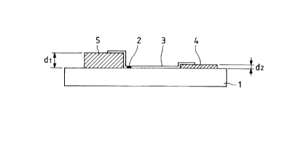
This embodiment is configured to show a first
basic structure as schematically illustrated in Figs.
lA and lB. Note that, in Figs. lA and lB, reference
numerals 1, 2 and 3 respectively denote a substrate, an
electron-emitting region and an electroconductive thin
film including an electron-emitting region, whereas
reference numerals 4 and 5 denote device electrodes.
Materials that can be used for the substrate 1
include quartz glass, glass contA; n; ng impurities such
as Na to a reduced concentration level, soda lime
glass, glass substrate realized by forming an SiO2 layer
on soda lime glass by means of sputtering, ceramic
substances such as alumina as well as Si.
While the oppositely arranged device electrodes 4
and 5 may be made of any highly conducting material,
- 23 ~1~&88~
preferred candidate materials include metals such as
Ni, Cr, Au, Mo, W, Pt, Ti, Al, Cu and Pd and their
alloys, printable conducting materials made of a metal
or a metal oxide selected from Pd, Ag, Ru02, Pd-Ag and
glass, transparent conducting materials such as
In203-SnO2 and semiconductor materials such as
polysilicon.
The distance L separating the device electrodes,
the length W1 of the device electrodes, the contour of
the electroconductive film 3 and other factors for
designing a surface conduction electron-emitting device
according to the invention may be determined depending
on the application of the device.
The distance L separating the device electrodes 4
and 5 is normally between several hundred angstroms and
several hundred micrometers, although it is determined
as a function of the performance of the aligner and the
specific etching technique used in the photolithography
process for the purpose of the invention as well as the
voltage to be applied to the device electrodes,
although a distance between several to several hundred
micrometers is preferable because such a distance
matches the exposing technique and the printing
technique to be used for preparing a large display
screen.
While the length W1 and the film thicknesses dl,
d2 of the device electrodes 4 and 5 are typically
- 24 _ 21~8~
determined as a function of the electric resistances of
the electrodes and other factors that may be involved
when a large number of such electron-emitting devices
are used, the length W1 is preferably between several
micrometers and hundreds of several micrometers and the
film thicknesses dl, d2 of the device electrodes 2 and
3 are between hundreds of several angstroms and several
micrometers.
A surface conduction electron-emitting device
according to the invention has an electron-emitting
region 2 located close to one of the device electrodes
(or the device electrode 5 in Figs. lA and lB). As
will be described in greater detail hereinafter, such
an electron-emitting region 2 can be formed by
differentiating the heights of the step portions of the
device electrodes. Such differentiation between the
step portions can be achieved by using films having
different thicknesses dl and d2 for the device
electrodes 5 and 4 respectively or, alternatively, by
forming an insulation layer typically made of SiO2 film
under either one of the device electrodes.
The height of the step portion of each of the
device electrodes is selected, taking the method of
preparing the electroconductive thin film 3 and the
morphology of the film 3 into consideration, in such
way that the electroconductive thin film 3 shows a
relatively high electric resistance and therefore a
- 25 - 21~ 8~ 6
relatively reduced thickness due to poor step coverage
or, if the electroconductive thin film is made of fine
particles as will be described hereinafter, a
relatively low density of fine particles in an area
located close to the step portion of the device
electrode having a greater thickness (or the step
portion of the device electrode 5 in Figs. lA and lB)
if compared with the rer~; ni ~g area of the
electroconductive thin film. The step portion of the
higher device electrode has a height typically more
than five times, preferably more than ten times, as
large as the thickness of the electroconductive thin
film 3.
The electroconductive thin film 3 is preferably a
fine particle film in order to provide excellent
electron-emitting characteristics. The thickness of
the electroconductive thin film 3 is determined as a
function of the electric resistance between the device
electrodes 4 and 5 and the parameters for the forming
operation that will be described hereinafter as well as
other factors and preferably between several and
several thousand angstroms, preferably between 10 and
500 angstroms. The electroconductive thin film 4
normally shows a resistance per unit surface area
between 102 and 107 Q/cm2.
The term a "fine particle film" as used herein
refers to a thin film constituted of a large number of
- 26 _ 21~8~
fine particles that may be loosely dispersed, tightly
arranged or mutually and randomly overlapping (to form
an island structure under certain conditions). If a
fine particle film is used, the particle size is
preferably between several and several hundred
angstroms, preferably between 10 and 200 angstroms.
By forming device electrodes having respective
step portions whose heights are different from each
other, the electroconductive thin film 3 that is
prepared in a subsequent step comes to show a good step
coverage relative to the device electrode 4 having a
low step portion and a poor step coverage relative to
the device electrode 5 having a high step portion.
Note that the area of the electroconductive thin film 3
that poorly covers the step portion is preferably
located close to the surface of the substrate.
The electroconductive thin film 3 is made of a
material selected from metals such as Pd, Ru, Ag, Au,
Ti, In, Cu, Cr, Fe, Zn, Sn, Ta, W and Pb, oxides such
as PdO, SnOz, In203, PbO and Sb203, borides such as HfB2,
ZrB2, LaB6, CeB6, YB4 and GdB4, carbides such as TiC,
ZrC, HfC, TaC, SiC and WC, nitrides such as TiN, ZrN
and HfN, semiconductors such as Si and Ge and carbon.
The electron-emitting region 2 contains fissures
and electrons are emitted from these fissures. The
electron-emitting region 2 containing such fissures and
the fissures themselves are produced as a function of
- 27 _ 21~8886
the thickness, the state and the material of the
electroconductive thin film 3 and the parameters for
carrying out an energization forming process for the
electron-emitting region 2.
As described above, an area of the
electroconductive thin film 3 is made to poorly covers
the step portion of one of the device electrodes having
a greater thickness at a position located close to the
surface of the substrate by selecting an appropriate
technique for preparing the electroconductive thin film
in a subsequent step. With this arrangement, fissures
can be generated preferentially in that area in the
process of energization forming, which will be
described hereinafter, to produce an electron-emitting
region. As shown in Figs. lA and lB, a substantially
linear electron-emitting region 2 is formed along the
straight step portion of the device electrode having a
greater thickness at a position close to the surface of
the substrate, although the location of the
electron-emitting region 2 is not limited to that of
Fig. lA or lB.
The fissures may contain electroconductive fine
particles having a diameter of several to hundreds of
several angstroms. The fine particles are part of some
or all of the elements constituting the
electroconductive thin film 3. Additionally, the
electron-emitting region 2 containing fissures and the
- 28 _ 21~8S~
neighboring areas of the electroconductive thin film 3
may contain carbon and carbon compounds.
Now, a method of manufacturing a surface
conduction electron-emitting device according to the
invention and illustrated in Figs. lA and lB will be
described by referring to Figs. 2A through 2C.
1) After thoroughly cleansing a substrate 1 with
detergent and pure water, a material is deposited on
the substrate 1 by means of vacuum deposition,
sputtering or some other appropriate technique for a
pair of device electrodes 4 and 5, which are then
produced by photolithography. Then, the material of
the electrodes is further deposited only on the device
electrode 5, masking the other device electrode 4, to
make the step portion of the device electrode 5 higher
than that of the device electrode 4 (Fig. 2A).
2) An organic metal thin film is formed on the
substrate 1 carrying thereon the pair of device
electrodes 4 and 5 by applying an organic metal
solution and leaving the applied solution for a given
period of time. The organic metal solution may contain
as a principal ingredient any of the metals listed
above for the electroconductive thin film 3.
Thereafter, the organic metal thin film is heated,
baked and subsequently subjected to a patterning
operation, using an appropriate technique such as
lift-off or etch;ng, to produce an electroconductive
- 29 -2158~
thin film 3 (Fig. 2B). While an organic metal solution
is used to produce a thin film in the above
description, an electroconductive thin film 3 may
alternatively be formed by vacuum deposition,
sputtering, chemical vapor phase deposition, dispersed
application, dipping, spinner or some other technique.
3) Thereafter, the device electrodes 4 and 5 are
subjected to a process referred to as "energization
forming". More specifically, the device electrodes 4
and 5 are electrically energized by means of a power
source (not shown) until a substantially linear
electron emitting region 3 is produced at a position of
the electroconductive thin film 3 near the step portion
of the device electrode 5 (Fig. 2C) as an area where
the electroconductive thin film is structurally
modified. In other words, the electron-emitting region
2 is a portion of the electroconductive thin film 3
that is locally destructed, deformed or transformed as
a result of energization forming to show a modified
structure.
Figs. 3A and 3B show two different pulse voltages
that can be used for energization forming.
The voltage to be used for energization forming
preferably has a pulse waveform. A pulse voltage
having a constant height or a constant peak voltage may
be applied continuously as shown in Fig. 3A or,
alternatively, a pulse voltage having an increasing
2158~38~
- 30 -
height or an increasing peak voltage may be applied as
shown in Fig. 3B.
Firstly, a pulse voltage having a constant height
~ill be described. In Fig. 3A, the pulse voltage has a
pulse width T1-and a pulse interval T2, which are
typically between 1 ~sec. and 10 msec. and between
10 ,usec. and 100 msec. respectively. The height of the
triangular wave (the peak voltage for the energization
forming operation) may be appropriately selected
depending on the profile of the surface conduction
electron-emitting device. The voltage is typically
applied for tens of several minutes in vacuum of an
appropriate degree. Note, however, that the pulse
waveform is not limited to triangular and a rectangular
or some other waveform may alternatively be used.
Now, a pulse voltage having an increasing height
will be described. Fig. 3B shows a pulse voltage whose
pulse height increases with time. In Fig. 3B, the
pulse voltage has an width Tl and a pulse interval T2
20 that are substantially similar to those of Fig. 3A.
The height of the triangular wave (the peak voltage for
the energization forming operation) is increased at a
rate of, for instance, O.lV per step. Note again that
the pulse waveform is not limited to triangular and a
rectangular or some other waveform may alternatively be
used.
The energization forming operation will be
- 31 _ 215~86
terminated as appropriately judged by measuring the
current running through the device electrodes when a
voltage that is sufficiently low and cannot locally
destroy or deform the electroconductive thin film 3 is
applied to the device during an interval T2 of the
pulse voltage. Typically the energization forming
operation is terminated when a resistance greater than
lM ohms is observed for the device current running
through the electroconductive thin film 3 while
applying a voltage of approximately O.lV to the device
electrodes.
4) After the energization forming operation, the
device is preferably subjected to an activation
process. An activation process is a process to be
carried out in order to dramatically change the device
current (film current) If and the emission current Ie.
In an activation process, a pulse voltage may be
repeatedly applied to the device in a vacuum
atmosphere. In this process, a pulse voltage is
repeatedly applied as in the case of energization
forming in an organic gas containing atmosphere. Such
an atmosphere may be produced by utilizing the organic
gas l~ ~; ni ng in a vacuum chamber after evacuating the
chamber by means of an oil diffusion pump or a rotary
pump or by sufficiently evacuating a vacuum chamber by
means of an ion pump and thereafter introducing the gas
of an organic substance into the vacuum. The gas
_ 32 - 2I588~6
pressure of the organic substance is determined as a
function of the profile of the electron-emitting device
to be treated, the profile of the vacuum chamber, the
type of the organic substance and other factors. The
organic subst~nc~ that can be suitably used for the
purpose of the activation process include aliphatic
hydrocarbons such as alkanes, alkenes and alkynes,
aromatic hydrocarbons, alcohols, aldehydes, ketones,
amines, organic acids such as, phenol, carbonic acids
and sulfonic acids. Specific examples include
saturated hydrocarbons expressed by general formula
CnH2n+2 such as methane, ethane and propane, unsaturated
hydrocarbons expressed by general formula CnH2n such as
ethylene and propylene, benzene, toluene, methanol,
ethanol, formaldehyde, acetaldehyde, acetone,
methylethylketone, methylamine, ethylamine, phenol,
formic acid, acetic acid and propionic acid. As a
result of this process, carbon and carbon compounds
contained in the atmosphere are deposited on the device
to remarkably change the device current If and the
emission current Ic.
The activation process is terminated whenever
appropriate, observing the device current If and the
emission current Ie. The pulse width, the pulse
interval and the pulse wave height are appropriately
selected.
For the purpose of the invention, carbon and
2 1 ~ 6
carbon compounds typically refer to graphite (including
so-called highly oriented pyrolytic graphite (HOPG),
pyrolitic graphite (PG) and glassy carbon (GC), of
which HOPG has a nearly perfect crystal structure of
graphite and PG contains crystal grains having a size
of about 200 angstroms and has a somewhat disturbed
crystal structure, while GC contains crystal grains
having a size as small as 20 angstroms and has a
crystal structure that is remarkably in disarray) and
non-crystalline carbon (including amorphous carbon and
a mixture of amorphous carbon and fine crystals of
graphite) and the thickness of film formed by
deposition is preferably less than 500 angstroms and
more preferably less than 300 angstroms.
5) A surface conduction electron-emitting device
according to the invention and have gone through the
above listed steps is preferably subjected to a
stabilizing step. This step is deslgned to evacuate
vacuum container arranged for manufacturing the device
to eliminate organic substances therefrom. Preferably,
an oil free vacuum apparatus is used to evacuate the
vacuum container so that it may not produce any oil
that can adversely affect the performance of the
electron-emitting device. Specific examples of oil
free vacuum apparatus that can be used for the purpose
of the invention include a sorption pump and an ion
pump.
~ 34 ~ 21~8~6
If an oil diffusion pump of a rotary pump is used
to evacuate the cont~iner to utilize the organic gas
generated from one or more than one ingredients the oil
of such a pump in the pr~e~;ng activation step, the
partial pressure of the oil ingredients has to be held
as low as possible. The partial pressure of the
organic gas within the vacuum container is preferably
less than lxlO~8Torr and more preferably less than
lxlO~10Torr under the condition where carbon and carbon
compounds are no longer deposited on the
electron-emitting device. For evacuating the vacuum
container, it is preferable that the entire container
is heated so that the molecules of the organic
substances adsorbed to the inner walls of the container
and the electron-emitting device may easily move away
therefrom and become removed from the container. The
heating operation may preferably be conducted at 80 to
200C for more than five hours, although values for
these parameters should be appropriately selected
depending on the size and shape of the vacuum
container, the configuration of the electron-emitting
device and other considerations. High temperature is
advantageous for causing the adsorbed molecules to move
away. While the temperature range of 80 to 200C is
selected to minimize the possible damage by heat to the
electron source to be prepared in the container, a
higher temperature may be recommended if the electron
_ 35 _ 21~888~
source is resistant against heat. It is also necessary
to keep the overall pressure in the vacuum container as
low as possible. It is preferably less than 1 to
3xlO~7Torr and more preferably less than lx10-8.
After completing the stabilizing step, the
electron-emitting device is preferably driven in an
atmosphere same as that in which said stabilizing
process is terminated, although a different atmosphere
may also be used. So long as the organic substances
are satisfactorily removed, a lower degree of vacuum
may be permissible for a stabilized operation of the
device.
With the use of such a vacuum condition, any
additional deposition of carbon and carbon compounds is
effectively prevented to stabilize both the device
current If and the emission current Ie.
Embodiment 2
Now, a second basic structure of surface
conduction electron-emitting device according to the
invention will be described.
In a surface conduction electron-emitting device
having this basic structure as shown in Figs. 4A and
4B, an electron-emitting region is formed close to
either one of a pair of device electrodes 4 and 5
having respective step portions whose heights are equal
to each other.
As seen from Figs. 4A and 4B, an electroconductive
- 36 ~ 2 15 8~86
thin film 3 is formed on the device electrode 5 and
under the other device electrode 4. Thus, a step is
produced on the electroconductive thin film only on the
device electrode 5 and, consequently, an
electron-emitting region 2 is formed at a position
close to the device electrode 5 as a result of
energization forming.
As described above by referring to the first
embodiment, the relationship between the height of the
device electrode 5 and the thickness of the
electroconductive thin film 3 is preferably such that
the device electrode 5 is more than five time,
preferably more than ten times, greater than the
thickness of the electroconductive thin film 3. The
ræ -; n; ng requirements of the configuration of the
first embodiment are mostly applicable to the second
embodiment.
While the device electrodes 4 and 5 may have
different heights, they are preferably equal in the
height from the manufacturing point of view.
A method of manufacturing a surface conduction
electron-emitting device having a configuration as
illustrated in Figs. 4A and 4B will be described by
referring to Figs. 31A through 31D.
1) After thoroughly cleansing an insulating
substrate 1 with detergent and pure water, a material
is deposited thereon by means of vacuum deposition,
_ 37 _ 2 15 8~ S6
sputtering or some other appropriate technique for
device electrodes, only a device electrode 5 is
produced on the insulating substrate 1 by
photolithography (Fig. 31A).
2) An organic metal thin film is formed on the
substrate 1 carrying thereon the device electrode 5 by
applying an organic metal solution and leaving the
applied solution for a given period of time. The
organic metal solution may contain as a principal
ingredient any of the metals listed above for the
electroconductive thin film 3. Thereafter, the organic
metal thin film is heated, baked and subsequently
subjected to a patterning operation, using an
appropriate technique such as lift-off or etching, to
produce an electroconductive thin film 3 (Fig. 31B).
While an organic metal solution is used to produce a
thin film in the above description, an
electroconductive thin film 3 may alternatively be
formed by vacuum deposition, sputtering, chemical vapor
phase deposition, dispersed application, dipping,
spinner or some other technique.
3) Another device electrode 4 is formed on the
electroconductive thin film 3 at a position separated
from the device electrode 5 (Fig. 31C). The height of
the device electrode 4 may be same as or different from
that of the device electrode 5.
4) Thereafter, the device electrodes 4 and 5 are
- 38 - 2 15 ~ ~ 8 ~
subjected to a process referred to as "energization
forming". More specifically, the device electrodes 4
and 5 are electrically energized by means of a power
source (not shown) until a substantially linear
electron-emitting region 3 is produced at a position of
the electroconductive thin film 3 near the step portion
of the device electrode 5 (Fig. 31D) as an area where
the electroconductive thin film is structurally
modified. In other words, the electron-emitting region
2 is a portion of the electroconductive thin film 3
that is locally destructed, deformed or transformed as
a result of energization forming to show a modified
structure.
The subsequent steps are same as those of
Embodiment 1 and therefore will not be described here
any further.
Embodiment 3
In a surface conduction electron-emitting device
according to the invention, an electron-emitting region
2 is formed at a position close to either one of a pair
of device electrodes (device electrode 5 in Figs. lA
and lB). Such an electron-emitting region can be
produced in either one of the first and second
manufacturing method according to the invention, which
will be described in greater detail hereinafter.
Now, a surface conduction electron-emitting device
according to the invention and illustrated in Figs. lA
- 39 - 21~8~6
and lB will be described by referring to Figs. 2A
through 2C that shows the device in different
manufacturing steps.
l) After thoroughly cleansing a substrate 1 with
detergent and pure water, a material is deposited on
the substrate 1 by means of vacuum deposition,
sputtering or some other appropriate technique for a
pair of device electrodes 4 and 5, which are then
produced by photolithography. Then, the material of
the electrodes is further deposited only on the device
electrode 5, masking the other device electrode 4, to
make the step portion of the device electrode 5 higher
than that of the device electrode 4 (Fig. 2A).
2) An organic metal thin film is formed on the
insulating substrate by spraying an organic metal
solution through a nozzle 33 with a mask member 32
interposed therebetween as shown in Fig. 6A. The
organic metal solution contains organic metal compounds
of the metals that are principal components of the
electroconductive thin film 3 to be formed there.
Thereafter, the organic metal thin film is heated and
baked to produce a patterned electroconductive thin
film 3 (Fig. 2B). Note that the components in Fig. 6A
that are same or similar to those of Figs. lA and lB
are denoted by the same reference symbols. In Fig. 6A,
reference numeral 31 denotes an area where organic
metal solution fine particles are applied and reference
- 40 21~ 8~C 6
numeral 34 denotes organic metal solution fine
particles.
While the organic metal solution is sprayed with a
mask member 32 interposed between the nozzle 33 and the
substrate 1 in order to omit an independent patterning
step in the above description, an electroconductive
thin film 3 may alternatively be formed without such a
mask member 32 by using an appropriate photolithography
technique such as lift-off or etching.
3) Thereafter, the device electrodes 4 and 5 are
subjected to a process referred to as "energization
forming". More specifically, the device electrodes 4
and 5 are electrically energized by means of a power
source (not shown) until a substantially linear
electron-emitting region 3 is produced at a position of
the electroconductive thin film 3 near the step portion
of the device electrode 5 (Fig. 2C) as an area where
the electroconductive thin film is structurally
modified. In other words, the electron-emitting region
2 is a portion of the electroconductive thin film 3
that is locally destructed, deformed or transformed as
a result of energization forming to show a modified
structure.
The steps subsequent to the energization forming
step are same as those of Embodiment 1 and therefore
will not be described here any further.
As described above, with the first method of
- 41 - 21~8886
manufacturing an electron-emitting device according to
the invention, a pair of device electrodes 4 and 5 are
so formed that their step portions show different
heights and a solution cont~i n; ng component elements of
the electroconductive thin film 3 is sprayed onto them
through a nozzle.
As the step portions of the device electrodes are
formed to show different heights with the first
manufacturing method, the electroconductive thin film 3
formed thereafter is made to show a good step coverage
for the device electrode 4 having a low step portion
and a poor step coverage for the device electrode 5
having a high step portion. Thus, in the above
described energization forming step, fissures can be
preferentially generated in the poor step coverage area
of the electroconductive thin film 3 to produce there
an electron-emitting region 2, which is substantially
linear and located close to the step portion of the
device electrode 5 as shown in Figs. lA and lB.
With the first manufacturing method of the
invention, an electroconductive thin film may be formed
so as to show a good step coverage for one of the
device electrodes and a poor step coverage for the
other device electrode by tilting the substrate 1 (or
the nozzle 33) of Fig. 6A as shown in Fig. 43 without
differentiating the heights of the step portions of the
device electrodes 4 and 5 unlike those of the device
- 42 -2 ~ 86
electrodes 4 and 5 of the electron-emitting device of
Figs. lA and lB. Note that the components in Fig. 43
that are similar to those of Fig. 6A are denoted by the
same reference symbols.
Thus, with such a manufacturing method, since the
electron-emitting device is prepared by means of a
process exactly same as that of preparing a device
comprising device electrodes whose step portions have
different heights, a substantially linear
electron-emitting region is formed in the energization
forming step at a position close to the step portion of
one of the device electrodes without differentiating
the heights of the step portions of the device
electrodes to consequently reduce the number of steps
necessary for preparing the device electrodes and make
the method advantageous.
Now, electrostatic spraying to be used for the
purpose of the invention will be described by referring
to Fig. 6B.
Fig. 6B schematically illustrates the principle of
electrostatic spraying. An electrostatic spraying
system that can be used for the purpose of the
invention comprises a nozzle 131 for spraying an
organic metal solution, a generator for atomizing an
organic metal solution 132, a tank 133 for storing an
organic metal solution, a high voltage DC power source
for electrically charging fine particles of organic
~ 43 ~ lS 8~8~
metal atomized in the generator 134 to a level of -10
to -lOOkV and a table 135 for carrying a substrate 1.
The nozzle 131 can be so operated as to
two-dimensionally scan the upper surface of the
substrate 1 at a constant rate. The substrate 1 is
grounded.
With the above arrangement, negatively charged
fine organic metal solution particles are sprayed
through the nozzle 131 and move with an accelerated
speed until they collide with the grounded substrate 1
and become deposited there to produce an organic metal
film that is more cohesive than a film produced by any
other spray method.
The electroconductive thin film can be subjected
to a patterning operation by means of photolithography
as described above by referring to Fig. 6A and, if a
mask member 32 as shown in Fig. 6A is used with
electrostatic spraying, a highly cohesive, tight and
uniform film can be produced by applying a voltage
between the nozzle 33 and the mask member 32 to
electrically charge fine particles of organic metal
solution 34 sprayed from the nozzle 33 to a level of 10
to lOOkV to accelerate them before they collide with
the substrate 1.
A surface conduction electron-emitting device
according to the invention can be prepared by a second
method of spraying a solution containing component
2 1~ 6
elements of the electroconductive thin film through a
nozzle, applying a voltage to a pair of device
electrode formed on a substrate.
More specifically, with the second method, unlike
the first basic arrangement of forming a pair of device
electrodes that are arranged asymmetrically (Example
l), a pair of device electrodes appear identical
physically appear identical as shown in Figs. 5A and 5B
and differentiated only by the electric potentials of
the electrodes so that the electroconductive thin film
formed from an organic metal solution sprayed through a
nozzle is made more cohesive and tight for the device
electrode with a lower electric potential than for the
device electrode with a higher electric potential and
provides a poor step coverage for the device electrode
with a higher electric potential. Consequently, a
substantially linear electron-emitting region 2 is
formed at a position close to the step portion of the
device electrode with a lower electrode as shown in
Figs. 5A and 5B.
For spraying a solution containing component
elements of the electroconductive thin film from a
nozzle with either one of the first and second
manufacturing methods, it is preferable to provide an
electric potential difference between the nozzle and
the substrate or enhance the adhesion between the
substrate and the device electrodes and the
_ 45 _ 2158~
electroconductive thin film to make the prepared
surface conduction electron-emitting device operate
more stably.
As described above, with a manufacturing method
according to the invention, a substantially linear
electron-emitting region is formed along one of the
device electrodes of a surface conduction
electron-emitting device at a position close to the
step portion of the electrode and the surface of the
substrate if the device electrodes are separated by a
large distance so that the electron-emitting region can
be prepared uniformly in terms of position and profile
and the surface conduction electron-emitting device
operates excellently as will be described hereinafter.
Additionally, since a nozzle is used to spray an
organic metal solution onto a substrate to produce an
electroconductive thin film with a manufacturing method
according to the invention and hence the substrate is
not rotated unlike the case where a spinner is used
with a conventional manufacturing method, it is
advantageous and effective when a large number of such
surface conduction electron-emitting devices are
arranged to produce an electron source because a large
substrate carrying a number of surface conduction
electron-emitting device is made to rotate with a risk
of damaging itself and an electron source and an image
forming apparatus incorporating such an electron source
46 21~888~
can be manufactured with relatively simple equipment.
Embodiment 4
Now, a fourth embodiment of surface conduction
electron-emitting device according to the invention and
having the third basic structure will be described
below. This embodiment of surface conduction
electron-emitting device comprises a pair of devlce
electrodes and an electroconductive thin film including
an electron-emitting region arranged close to one of
the device electrodes and additionally provided with a
control electrode. In this embodiment, the control
electrode may be arranged on one of the device
electrodes or, alternatively, it may be arranged at a
peripheral area of the device electrode or the electro-
conductive thin film.
Figs. 7A and 7B show a surface conduction
electron-emitting device according to the invention
where a control electrode is arranged on one of the
device electrodes. Referring to Figs. 7A and 7B, the
surface conduction electron-emitting device comprises a
substrate 1, an electroconductive thin film 3 including
an electron-emitting region 2, a pair of device
electrodes 4 and 5, an insulation layer 6 and a control
electrode 7.
The control electrode is arranged on the device
electrode 5 and the electroconductive thin film 3 with
an insulation layer 6 interposed therebetween and made
_ 47 ~1~888~
of a material popularly used for electrodes.
Possible relations among the electric potentials
of the components for driving the surface conduction
electron-emitting device will be described below.
The device electrode 5 is held to a potential
lower than that of the device electrode 4 and the
control electrode 7 is held to a potential higher than
that of the device electrode 4.
Under this condition, electrons emitted from the
electron-emitting region 2 located close to the device
electrode 5 move toward an anode (not shown), following
a trajectory directed from the lower potential device
electrode 5 to the higher potential device electrode 4
as described earlier and, since the control electrode 7
is located close to the electron-emitting region 2, the
moving electrons are effectively effected by the
electric potential of the control electrode 7. More
specifically, since the electric potential of the
control electrode 7 is higher than the device
electrodes, the trajectory of electrons is modified so
as to make the moving electrons to be less attracted by
the electroconductive thin film 3 and the device
electrode 4 and more effectively drawn toward the
anode. As a result, the rate of electron emission
increases as compared with that of electron emission
when the control electrode 7 is not provided. If, on
the other hand, the electric potential of the control
2 1 ~ ~ ~ 8 6
electrode 7 is made lower than that of the device
electrode 4 and equal to that of the device electrode
5, the net effect will be equivalent to the one
obtained when the device electrode 5 is made tall to
improve the convergence of electrons.
If the electric potential of the device electrode
5 is made higher than that of the device electrode 4
and that of the control electrode 7 is made equal to
that of the device electrode 4, electrons emitted from
the electron-emitting region 2 located close to the
device electrode 5 toward the device electrode 5 are
effectively cut off by the control electrode 7.
Since the electron-emitting region is located
close to one of the device electrodes and the control
electrode 7 is arranged on that device electrode with
an insulation layer interposed therebetween, the
trajectory of electrons emitted from the
electron-emitting region 2 can be effectively
controlled by means of the control electrode 7. While
the control electrode has an end surface that agrees
with those of the device electrode 5 and the insulation
layer 6 in Fig. 7A, the profile of the control
electrode 7 is not limited thereto and those of the
insulation film 6 and the control electrode 7 may be
shifted to the left from that of the device electrode 5
in Fig. 7A (Fig. 12).
Embodiment 5
_ 49 _ 215~
In this embodiment, the control electrode is
formed on the substrate as shown in Figs. 9A and 9B.
The components that are same or similar to those of the
embodiment of Figs. 7A and 7B are denoted by the same
reference symbols. In the following description, X
denotes the direction of L1 and Y denotes a direction
perpendicular to X.
Referring to Figs. 9A and 9B, the control
electrode 7 is formed on the substrate 1. The control
electrode 7 may be placed between the device electrodes
as shown or, alternatively, it may be so arranged as to
surround the device electrodes and the
electroconductive thin film. It may be electrically
connected to either one of the device electrodes.
Assume here that the control electrode is arranged in a
manner as shown in Figs. 9A and 9B and the electric
potential of the device electrode 5 is lower than that
of the device electrode 4 while the electric potential
of the control electrode 7 is equal to that of the
device electrode 5.
Then, electrons emitted from the electron-emitting
region 2 move toward the higher potential device
electrode 4 along the X-direction and, if no voltage is
applied to the control electrode 7, spread in the
Y-direction. However, since the control electrode 7 is
held to a relatively low electric potential, the spread
of electrons in the Y-direction is suppressed to
~ 50 - 2 13 8~
improve the convergence. Additionally, if no voltage
is applied to the control electrode 7 and the substrate
is electrically insulated, the electric potential of
the insulated substrate is unstable and emitted
electrons are affected by the electric potential of the
substrate to swerve the trajectory of emitted electrons
so that, if the electron-emitting device is used in an
image display apparatus, the light emitting spot of the
display screen of the apparatus that provides the
target of electrons from the èlectron-emitting device
may change its profile to degrade the image displayed
on the screen. Such a problem is eliminated by
applying an appropriate voltage to the control
electrode 7 to stabilize the electric potential of the
substrate 1 and hence the trajectory of emitted
electrons and consequently improve the quality of the
image on the screen. Note that the control electrode 7
may alternatively be arranged on one of the device
electrodes and around the device electrodes and the
electroconductive thin film.
Now, a method of manufacturing an surface
conduction electron-emitting device comprising a
control electrode 7 will be described below by
referring to a case where the control electrode is
formed on one of the device electrodes and another case
where the control electrode is formed on the substrate.
Case 1: The control electrode is formed on one of
- 51 ~ 2 1~8
the device electrodes.
A surface conduction electron-emitting device
shown in Figs. 7A and 7B is manufactured by a method as
illustrated in Figs. 8A through 8D.
1) After thoroughly cleansing a substrate 1 with
detergent and pure water, a material is deposited on
the substrate 1 by means of vacuum deposition,
sputtering or some other appropriate technique for a
pair of device electrodes 4 and 5, which are then
produced by photolithography. Then, the material of
the electrodes is further deposited only on the device
electrode 5, masking the other device electrode 4, to
make the step portion of the device electrode 5 higher
than that of the device electrode 4 (Fig. 3A).
2) An organic metal thin film is formed on the
substrate 1 carrying thereon the pair of device
electrodes 4 and 5 by applying an organic metal -~
solution and leaving the applied solution for a given
period of time. The organic metal solution may contain
as a principal ingredient any of the metals listed
above for the electroconductive thin film 3.
Thereafter, the organic metal thin film is heated,
baked and subsequently subjected to a patterning
operation, using an appropriate technique such as
lift-off or etching, to produce an electroconductive
thin film 3 (Fig. 8B). While an organic metal solution
is used to produce a thin film in the above
- 52 -
2 1~ 8 ~
description, an electroconductive thin film 3 may
alternatively be formed by vacuum deposition,
sputtering, chemical vapor phase deposition, dispersed
application, dipping, spinner or some other technique.
3) After depositing a material for an insulation
layer on the substrate 1 that carries a pair of device
electrodes 4 and 5 and an electroconductive thin ilm 3
by vacuum deposition or sputtering, a mask is formed
only on the device electrode 5 having a step portion
higher than that of the other device electrode 4 by
photolithography and an insulation layer 6 having a
desired profile is produced by etching, utilizing the
mask. Note that the insulation layer 6 does not
entirely cover the device electrode 5 and should have a
profile that provides appropriate electric contact
necessary for applying a voltage to the device
electrode. Then, all the area other than the
insulation layer 6 is masked and a control electrode 7
is formed on the insulation layer 6 by vacuum
deposition or sputtering (Fig. 8C).
4) Thereafter, the device electrodes 4 and 5 are
subjected to a process referred to as "energization
forming". More specifically, the device electrodes 4
and 5 are electrically energized by means of a power
source (not shown) until a substantially linear
electron-emitting region 3 is produced at a position of
the electroconductive thin film 3 near the step portion
21~,8~8~
of the device electrode 5 (Fig. 8D) as an area where
the electroconductive thin film is structurally
modified. In other words, the`electron-emitting region
2 is a portion of the electroconductive thin film 3
that is locally destructed, deformed or transformed as
a result of energization forming to show a modified
structure.
The steps subsequent to the energization forming
step are same as those of Embodiment 1 and therefore
will not be described here any further.
Case 2: The control electrode is formed on the
substrate.
A surface conduction electron-emitting device
shown in Figs. 9A and 9B is manufactured by a method as
illustrated in Figs. lOA through lOC.
1) After thoroughly cleansing a substrate 1 with
detergent and pure water, a material is deposited on
the substrate 1 by means of vacuum deposition,
sputtering or some other appropriate technique for a
pair of device electrodes 4 and 5, which are then
produced by photolithography. Then, the material of
the electrodes is further deposited only on the device
electrode 5, masking the other device electrode 4, to
make the step portion of the device electrode 5 higher
than that of the device electrode 4. At the same time,
a control electrode 7 is formed on the insulating
substrate 1 by photolithography like the device
- 54 -
2 1 ~
electrodes 4 and 5 (Fig. lOA).
2) An organic metal thin film is formed on the
substrate 1 carrying thereon the pair of device
electrodes 4 and 5 by applying an organic metal
solution and leaving the applied solution for a given
period of time. The organic metal solution may contain
as a principal ingredient any of the metals listed
above for the electroconductive thin film 3.
Thereafter, the organic metal thin film is heated,
baked and subsequently subjected to a patterning
operation, using an appropriate technique such as
lift-off or etching, to produce an electroconductive
thin film 3 (Fig. lOB). While an organic metal
solution is used to produce a thin film in the above
description, an electroconductive thin film 3 may
alternatively be formed by vacuum deposition,
sputtering, chemical vapor phase deposition, dispersed
application, dipping, spinner or some other technique.
3) Thereafter, the device electrodes 4 and 5 are
subjected to a process referred to as "energization
forming". More specifically, the device electrodes 4
and 5 are electrically energized by means of a power
source (not shown) until a substantially linear
electron emitting-region 3 is produced at a position of
the electroconductive thin film 3 near the step portion
of the device electrode 5 (Fig. lOC) as an area where
the electroconductive thin film is structurally
~ 55 ~ 21~ 88~
modified. In other words, the electron-emitting region
2 is a portion of the electroconductive thin film 3
that is locally destructed, deformed or transformed as
a result of energization forming to show a modified
structure.
The steps subsequent to the energization forming
step are same as those of Embodiment 1 and therefore
will not be described here any further.
The performance of a surface conduction
electron-emitting device according to the invention and
manufactured by a method as described above can be
determined in a manner as described below.
Fig. 11 is a schematic block diagram of a gauging
system for determining the performance of an electron-
emitting device of the type under consideration.Firstly, this gauging system will be described.
Referring to Fig. 11, the components that are same
as those of Figs. lA and lB are denoted by the same
reference symbols. Otherwise, the gauging system has a
power source 51 for applying a device voltage Vf to the
device, an ammeter 50 for metering the device current
If running through the thin film 3 between the device
electrodes 4 and 5, an anode 54 for capturing the
emission current Ie produced by electrons emitted from
the electron-emitting region of the device, a high
voltage source 53 for applying a voltage to the anode
54 of the gauging system and another ammeter 52 for
- 56 - 2158~
metering the emission current Ie produced by electrons
emitted from the electron-emitting region 2 of the
device. Reference numerals 55 and 56 respectively
denotes a vacuum apparatus and a vacuum pump.
The surface conduction electron-emitting device to
be tested, the anode 54 and other components are
disposed within the vacuum apparatus 55, which is
provided with instruments including a vacuum gauge and
other pieces of equipment necessary for the gauging
system so that the performance of the surface
conduction electron-emitting device or the electron
source in the chamber may be properly tested.
The vacuum pump 56 is provided with an ordinary
high vacuum system comprising a turbo pump or a rotary
pump or an oil-free high vacuum system comprising an
oil-free pump such as a magnetic levitation turbo pump
or a dry pump and an ultra-high vacuum system
comprising an ion pump. The entire vacuum apparatus 55
and the substrate of the electron source held therein
can be heated to 250C by means of a heater (not
shown). Note that the display panel (201 of Fig. 17)
of an image forming apparatus according to the
invention can be configured as such a gauging system.
Thus, all the processes from the energization
forming process on can be carried out with this gauging
system.
For determining the performance of a surface
21~8~86
conduction electron-emitting device according to the
invention, a voltage between 1 and lOkV may be applied
to the anode 54 of the gauging system, which is spaced
apart from the electron-emitting device by distance H
which is between 2 and 8mm.
Note that the performance of a surface conduction
electron-emitting device as illustrated in Figs. 7A and
7B or Figs. 9A and 9B is determined by using a power
source (not shown) for applying a voltage to the
control electrode 7 (not shown).
Fig. 13 shows a graph schematically illustrating
the relationship between the device voltage Vf and the
emission current Ie and the device current If typically
observed by the gauging system. Note that different
units are arbitrarily selected for Ie and If in Figs.
8A through 8D in view of the fact that Ie has a
magnitude by far smaller than that of If. Note that
both the vertical and transversal axes of the graph
represent a linear scale.
As seen in Fig. 13, an electron-emitting device
according to the invention has three remarkable
features in terms of emission current Ie, which will be
described below.
Firstly, an electron-emitting device according to
the invention shows a sudden and sharp increase in the
emission current Ie when the voltage applied thereto
exceeds a certain level (which is referred to as a
- 58 -
213~
threshold voltage hereinafter and indicated by Vth in
Fig. 13), whereas the emission current Ie is
practically undetectable when the applied voltage is
found lower than the threshold value Vth~ Differently
stated, an electron-emitting device according to the
invention is a non-linear device having a clear
threshold voltage Vth to the emission current Ie.
Secondly, since the emission current Ie is highly
dependent on the device voltage Vf, the former can be
effectively controlled by way of the latter.
Thirdly, the emitted electric charge captured by
the anode 54 is a function of the duration of time of
application of the device voltage Vf. In other words,
the amount of electric charge captured by the anode 54
can be effectively controlled by way of the time during
which the device voltage Vf is applied.
The relationship indicated by the solid line in
Fig. 13 represents that both the emission current Ie
and the device current If show a monotonically-
increasing characteristic (hereinafter referred to asMI characteristic) relative to the device voltage Vf
but the device current If can show a
voltage-controlled-negative-resistance characteristic
(hereinafter referred to as VCNR characteristic) (not
shown). The electron-emitting device shows either of
the two characteristics dep~n~;ng on the method used
for manufacturing it, the parameters of the gauging
~ 59 ~ 2l58~ 86
system and other factors. Note that, if the device
current If shows a VCNR characteristic to the device
voltage Vf, the emission current Ie shows an MI
characteristic relative to the device voltage Vf.
Because of the above remarkable characteristic
features, it will be understood that the
electron-emitting behavior of an electron source
comprising a plurality of electron-emitting devices
according to the invention and hence that of an
image-forming apparatus incorporating such an electron
source can easily be controlled in response to the
input signal. Thus, such an electron source and an
image-forming apparatus may find a variety of
applications.
An electron source according to the invention can
be realized by arranging surface conduction
electron-emitting devices, which will be described
below.
For instance, a number of electron-emitting
devices may be arranged in a ladder-like arrangement to
realize an electron source as described earlier by
referring to the prior art. Alternatively, an electron
source according to the invention may be realized by
arranging n Y-directional wires on m X-directional
wires with an interlayer insulation layer interposed
therebetween and placing a surface conduction
electron-emitting device close to each crossing of the
- 60 ~~15~ 86
wires, the pair of electrodes of device being connected
to the corresponding X- and Y-directional wires
respectively. This arrangement is referred to as
simple matrix wiring arrangement, which will be
described hereinafter in detail.
Because of the basic characteristics of a surface
conduction electron-emitting device as described above,
the rate at which the device emit electrons can be
controlled for by controlling the wave height and the
wave width of the pulse voltage applied to the opposite
electrodes of the device above the threshold voltage
level if the applied device voltage Vf exceeds the
threshold voltage Vth. On the other hand, the device
does not practically emit any electron below the
threshold voltage Vth. Therefore, regardless of the
number of electron-emitting devices arranged in an
apparatus, desired surface conduction electron-emitting
devices can be selected and controlled for electron
emission in response to an input signal by applying a
pulse voltage to each of the selected devices if a
simple matrix wiring arrangement is employed.
An electron source having a simple matrix wiring
arrangement is realized on the basis of the above
simple principle. Fig. 14 is a shematic plan view of
an electron source according to the invention and
having a simple matrix wiring arrangement.
In Fig. 14, the electron source comprises a
- 61 ~lS8~8~
substrate 1 which is typically made of a glass panel
and has a profile that depends on the number and the
application of the surface conduction electron-emitting
devices 104 arranged thereon.
There are provided a total of m X-directional
wires 102, which are donated by Dxl, Dx2, ..., Dxm and
made of an electroconductive metal produced by vacuum
deposition, printing or sputtering. These wires are so
designed in terms of material, thickness and width
that, if necessary, a substantially equal voltage may
be applied to the surface conduction electron-emitting
devices.
A total of n Y-directional wires are arranged and
donated by Dyl, Dy2, ..., Dyn, which are similar to the
X-directional wires in terms of material, thickness and
width.
An interlayer insulation layer (not shown) is
disposed between the m X-directional wires and the n
Y-directional wires to electrically isolate them from
each other. Both m and n are integers.
The interlayer insulation layer (not shown) is
typically made of SiOz and formed on the entire surface
or part of the surface of the insulating substrate 1 to
show a desired contour by means of vacuum deposition,
printing or sputtering. The thickness, material and
manufacturing method of the interlayer insulation layer
are so selected as to make it withstand the potential
- 62 -~1~8~
difference between any of the X-directional wires 102
and any of the Y-directional wires 103 observable at
the crossing thereof. Each of the X-directional wires
102 and the Y-directional wires 103 is drawn out to
form an external terminal.
The oppositely arranged electrodes (not shown) of
each of the surface conduction electron-emitting
devices 104 are connected to related one of the m
X-directional wire 102 and related one of the n
Y-directional wires 103 by respective connecting wires
105 which are made of an electroconductive metal and
formed by means of an appropriate technique such as
vacuum deposition, printing or sputtering. In view of
the method used for driving the electron source, which
will be described hereinafter, the electron-emitting
region of each surface conduction electron-emitting
device is preferably formed close to the device
electrode that is connected to the corresponding
X-directional wire 102.
The electroconductive metal material of the device
electrodes and that of the m X-directional wires 102,
the n Y-directional wires 103 and the connecting wires
105 may be same or contain a common element as an
ingredient. Alternatively, they may be different from
each other. These materials may be appropriately
selected typically from the candidate materials listed
above for the device electrodes. If the device
215~86
electrodes and the connecting wires are made of a same
material, they may be collectively called device
electrodes without discriminating the connecting wires.
The surface conduction electron-emitting devices 104
may be formed either on the substrate 1 or on the
interlayer insulation layer (not shown).
As will be described in detail hereinafter, the
X-directional wires 102 are electrically connected to a
scan signal application means (not shown) for applying
a scan signal to a selected row of surface conduction
electron-emitting devices 104.
On the other hand, the Y-directional wires 103 are
electrically connected to a modulation signal
generation means (not shown) for applying a modulation
signal to a selected column of surface conduction
electron-emitting devices 104 and modulating the
selected column according to an input signal. Note
that the drive signal to be applied to each surface
conduction electron-emitting device is expressed as the
voltage difference of the scan signal and the
modulation signal applied to the device.
Now, an electron source substrate comprising
surface conduction electron-emitting devices having the
third basic structure of the present invention will be
described by referring to Fig. 15. In Fig. 15,
reference numerals 1, 102 and 103 respectively denote
an electron source substrate, an X-directional wire and
- 64 - 215 8886
a Y-directional wire, whereas reference numerals 106,
104 and 105 respectively denote a wire for a control
electrode, a surface conduction electron-emitting
device and a connecting wire.
In Fig. 15, the electron source substrate 1 is
typically made of a glass panel and has a profile that
depends on the number and the application of the
surface conduction electron-emitting devices arranged
thereon.
There are provided a total of m X-directional
wires 102, which are also donated by Dxl, Dx2, ..., Dxm
and made of an electroconductive metal produced by
vacuum deposition, printing or sputtering. These wires
are so designed in terms of material, thickness and
width that, if necessary, a substantially equal voltage
may be applied to the surface conduction
electron-emitting devices. A total of n Y-directional
wires 103 are arranged and also donated by Dyl, Dy2,
..., Dyn, which are similar to the X-directional wires
102 in terms of material, thickness and width. There
are also a total of m wires for control electrodes 106
also denoted by G1, G2, ..., Gm and arranged like the
X-directional wires 102. Interlayer insulation layers
(not shown) are disposed so as to electrically isolate
the m X-directional wires 102, the m wires for control
electrodes 106 and the n Y-directional wires 103 from
each other. (Both m and n are integers.)
- 65 - 21588~6
The interlayer insulation layers (not shown) are
typically made of SiO2 and formed on the entire surface
or part of the surface of the insulating substrate 1
carrying the X-directional wires 102 and the wired for
the control electrodes 106 to show a desired contour by
means of vacuum deposition, printing or sputtering.
The thickness, material and manufacturing method of the
interlayer insulation layers are so selected as to make
it withstand the potential difference between any of
the X-directional wires 102 and the wires for the
control electrode 106 and any of the Y-directional
wires 103 observable at the crossing thereof. Each of
the X-directional wires 102, the wires for the control
electrodes 106 and the Y-directional wires 103 is drawn
out to form an external terminal.
The oppositely arranged device electrodes and the
control electrode (not shown) of each of the surface
conduction electron-emitting devices 104 are connected
to related one of the m X-directional wires 102 and
related one of the n Y-directional wires 103 by
respective connecting wires 105 which are made of an
electroconductive metal and formed by means of an
appropriate technique such as vacuum deposition,
printing or sputtering.
The electroconductive metal material of the device
electrodes and the control electrode of each surface
conduction electron-emitting device and that of the m
21~8~
X-directional wires 102, the n Y-directional wires 103
and the m wires for the control electrodes 106 may be
same or contain a common element as an ingredient.
Alternatively, they may be different from each other.
These materials may be appropriately selected typically
from the candidate materials listed above for the
device electrodes. If the device electrodes and the
connecting wires are made of a same material, they may
be collectively called device electrodes without
discriminating the connecting wires. The surface
conduction electron-emitting devices may be formed
either on the substrate 1 or on the interlayer
insulation layer (not shown).
As will be described in detail hereinafter, the
X-directional wires 102 and the wires for the control
electrodes 106 are electrically connected to a scan
signal application means (not shown) for applying a
scan signal to a selected row of surface conduction
electron-emitting devices 104.
On the other hand, the Y-directional wires 103 are
electrically connected to a modulation signal
generation means (not shown) for applying a modulation
signal to a selected column of surface conduction
electron-emitting devices 104 and modulating the
selected column according to an input signal.
Note that the drive signal to be applied to each
surface conduction electron-emitting device is
- 67 ~ 215 8~g~
expressed as the voltage difference of the scan signal
and the modulation signal applied to the device.
Now, another electron source substrate comprising
surface conduction electron-emitting devices having the
third basic structure of the present invention will be
described by referring to Fig. 16.
In Fig. 16, the components that are same or
similar to those of Fig. 15 are denoted by the same
reference symbols. The electron source substrate of
Fig. 16 differs from that of Fig. 15 in that the wires
for the control electrodes 106 formed on the respective
control electrodes 7 are emitted and the control
electrodes 7 are connected to the corresponding
X-directional wires 102. With this arrangement, the
number of manufacturing steps can be reduced if
compared with the substrate of Fig. 15.
Now, still another electron source substrate
comprising surface conduction electron-emitting devices
having the third basic structure of the present
invention will be described by referring to Fig. 48.
In Fig. 48, reference numerals 1, 102 and 103
respectively denote an electron source substrate, an
X-directional wire and a Y-directional wire, whereas
reference numerals 106, 104 and 105 respectively denote
a wire for a control electrode, a surface conduction
electron-emitting device and a connecting wire.
In Fig. 48, the electron source substrate 1 is
- 68 - 2 15 S~ ~
typically made of a glass panel and has a profile that
depends on the number and the application of the
- surface conduction electron-emitting devices arranged
thereon.
There are provided a total of m X-directional
wires 102, which are also donated by Dxl, Dx2, ..., Dxm
and made of an electroconductive metal produced by
vacuum deposition, printing or sputtering. These wires
are so designed in terms of material, thickness and
width that, if necessary, a substantially equal voltage
may be applied to the surface conduction
electron-emitting devices. A total of n Y-directional
wires 103 are arranged and also donated by Dyl, Dy2,
..., Dyn, which are similar to the X-directional wires
102 in terms of material, thickness and width. There
are also a total of m wires for control electrodes 106
also denoted by Gl, G2, ..., Gm and arranged
alternately and in parallel with the X-directional
wires 102. Interlayer insulation layers (not shown)
are disposed so as to electrically isolate the m
X-directional wires 102, the m wires for control
electrodes 106 and the n Y-directional wires 103 from
each other. (Both m and n are integers.)
The interlayer insulation layers (not shown) are
typically made of SiO2 and formed on the entire surface
or part of the surface of the insulating substrate 1
carrying the X-directional wires 102 and the wired for
- 69 ~ 21~ ~8 86
the control electrodes 106 to show a desired contour by
means of vacuum deposition, printing or sputtering.
The thickness, material and manufacturing method of the
interlayer insulation layers are so selected as to make
it withstand the potential difference between any of
the X-directional wires 102 and the wires for the
control electrode 106 and any of the Y-directional
wires 103 observable at the crossing thereof. Each of
the X-directional wires 102, the wires for the control
electrodes 106 and the Y-directional wires 103 is drawn
out to form an external terminal.
The oppositely arranged device electrodes and the
control electrode (not shown) of each of the surface
conduction electron-emitting devices 104 are connected
to related one of the m X-directional wires 102 and
related one of the n Y-directional wires 103 by
respective connecting wires 105 which are made of an
electroconductive metal and formed by means of an
appropriate technique such as vacuum deposition,
printing or sputtering.
The electroconductive metal material of the device
electrodes and the control electrode of each surface
conduction electron-emitting device and that of the m
X-directional wires 102, the n Y-directional wires 103
and the m wires for the control electrodes 106 may be
same or contain a common element as an ingredient.
Alternatively, they may be different from each other.
Z158~86
These materials may be appropriately selected typically
from the candidate materials listed above for the
device electrodes. If the device electrodes and the
connecting wires are made of a same material, they may
be collectively called device electrodes without
discriminating the connecting wires. The surface
conduction electron-emitting devices may be formed
either on the substrate 1 or on the interlayer
insulation layer (not shown).
As will be described in detail hereinafter, the
X-directional wires 102 and the wires for the control
electrodes 106 are electrically connected to a scan
signal application means (not shown) for applying a
scan signal to a selected row of surface conduction
electron-emitting devices 104.
On the other hand, the Y-directional wires 103 are
electrically connected to a modulation signal
generation means (not shown) for applying a modulation
signal to a selected column of surface conduction
electron-emitting devices 104 and modulating the
selected column according to an input signal.
Note that the drive signal to be applied to each
surface conduction electron-emitting device is
expressed as the voltage difference of the scan signal
and the modulation signal applied to the device.
Now, another electron source substrate comprising
surface conduction electron-emitting devices having the
21S~6
fourth basic structure of the present invention will be
described by referring to Fig. 57.
In Fig. 57, the components that are same or
similar to those of Fig. 48 are denoted by the same
reference symbols. The electron source substrate of
Fig. 57 differs from that of Fig. 48 in that the wires
for the control electrodes 106 formed on the respective
control electrodes 7 are emitted and the control
electrodes 7 are connected to the correspon~i~g
X-directional wires 102. With this arrangement, the
number of manufacturing steps can be reduced if
compared with the substrate of Fig. 15.
Now, an image forming apparatus comprising an
electron source with a simple matrix wiring arrangement
according to the invention will be described by
referring to Figs. 17 through 19, of which Fig. 17 is a
schematic perspective view of the display panel 201 of
the image forming apparatus and Figs. 18A and 18B are
two possible configurations of the fluorescent film 114
of the display panel, whereas Fig. 19 is a block
diagram of a drive circuit for displaying television
images according to NTSC television signals.
In Fig. 17, reference numeral 1 denotes an
electron source substrate carrying thereon a plurality
of surface conduction electron-emitting devices
according to the invention. Otherwise, the display
panel comprises a rear plate 111 rigidly holding the
_ 72 ~ 21~ 8~ $6
electron source substrate 1, a face plate 116 prepared
by laying a fluorescent film 114 that operates as an
image forming member and a metal back 115 on the inner
surface of a glass substrate 113 and a support frame
112. The rear plate 111, the support frame 112 and the
face plate 116 are bonded together by applying frit
glass to the junctions of the these components and
baked to 400 to 500C for more than 10 minutes in the
atmosphere or in nitrogen and hermetically and
airtightly sealed to produce an envelope 118.
In Fig. 17, reference numeral 104 denotes an
electron-emitting device and reference numerals 102 and
103 respectively denote the X-directional wiring and
the Y-directional wiring connected to the respective
device electrodes 4 and 5 of each electron-emitting
device (Figs. lA and lB).
While the envelope 118 is formed of the face plate
116, the support frame 112 and the rear plate 111 in
the above described embodiment, the rear plate 31 may
be omitted if the substrate 1 is strong enough by
itself because the rear plate 111 is provided mainly
for reinforcing the substrate 1. If such is the case,
an independent rear plate 111 may not be required and
the substrate 1 may be directly bonded to the support
frame 112 so that the envelope 118 is constituted of a
face plate 116, a support frame 112 and a substrate 1.
The overall strength of the envelope 118 may be
- 73 - 21~
increased by arranging a number of support members
called spacers (not shown) between the face plate 116
and the rear plate 111.
Figs. 18A and 18B schematically illustrate two
possible arrangements of fluorescent film. While the
fluorescent film 114 comprises only a single
fluorescent body 122 if the display panel is used for
showing black and white pictures, it needs to comprise
for displaying color pictures black conductive members
121 and fluorescent bodies 122, of which the former are
referred to as black stripes (Fig. 18A) or members of a
black matrix (Fig. 18B) depending on the arrangement of
the fluorescent bodies. Black stripes or members of a
black matrix are arranged for a color display panel so
that the fluorescent bodies 122 of three different
primary colors are made less discriminable and the
adverse effect of reducing the contrast of displayed
images of external light is minimized in the
fluorescent film 114 by blackening the surrounding
areas. While graphite is normally used as a principal
ingredient of the black stripes, other conductive
material having low light transmissivity and
reflectivity may alternatively be used.
A precipitation or printing technique may suitably
be used for applying a fluorescent material to form
fluorescent bodies 122 on the glass substrate 113
regardless of black and white or color display.
~ 74 ~ 2158~8 6
An ordinary metal back 115 is arranged on the
inner surface of the fluorescent film 114 as shown in
Fig. 17. The metal back 115 is provided in order to
enhance the luminance of the display panel by causing
the rays of light emitted from the fluorescent bodies
122 (Fig. 18A or 18B) and directed to the inside of the
envelope to mirror-reflect toward the face plate 116,
to use it as a high voltage electrode Hv for applying
an accelerating voltage to electron beams and to
protect the fluorescent bodies 122 against damages that
may be caused when negative ions generated inside the
envelope 118 collide with them. It is prepared by
smoothing the inner surface of the fluorescent film 114
(in an operation normally called "filming") and forming
an Al film thereon by vacuum deposition after forming
the fluorescent film 114.
A transparent electrode (not shown) may be formed
on the face plate 116 facing the outer surface of the
fluorescent film 114 in order to raise the conductivity
of the fluorescent film 34.
Care should be taken to accurately align each set
of color fluorescent bodies 122 and an
electron-emitting device 104, if a color display is
involved, before the above listed components of the
envelope are bonded together.
The envelope 118 is evacuated to a degree of
vacuum of 10-6 to 10~7Torr or higher degree via an
~ 75 2 1~8886
evacuation pipe (not shown) and hermetically sealed.
More specifically, the inside of the envelope 118
is evacuated by means of an ordinary vacuum system
typically comprising a rotary pump or a turbo pump to a
degree of vacuum of about 10~6Torr and the surface
conduction electron-emitting devices in the inside are
subjected to an energization forming step and an
activation step to produce electron-emitting regions 2
as described earlier by applying a voltage to the
device electrodes 4 and 5 via the external terminals
Dxl through Dxm and Dyl through Dyn. Thereafter, the
vacuum system is switched to an ultra-high vacuum
system typically comprising an ion pump, while baking
the apparatus at 80 to 200C. A getter process may be
conducted in order to maintain the achieved degree of
vacuum in the inside of the envelope 118 immediately
before or after it is hermetically sealed. In a getter
process, a getter arranged at a predetermined position
in the envelope 118 is heated by means of a resistance
heater or a high frequency heater to form a film by
vapor deposition. A getter typically contains Ba as a
principal ingredient and can maintain a high degree of
vacuum by the adsorption effect of the vapor deposition
film.
The above described display panel 201 can be
driven by a drive circuits as shown in Fig. 19. In
Fig. 19, reference numeral 201 denotes a display panel.
- 215~8~
Otherwise, the circuit comprises a scan circuit 202, a
control circuit 203, a shift register 204, a line
memory 205, a synchronizing signal separation circuit
206 and a modulation signal generator 207. Vx and Va
in Fig. 19 denote DC voltage sources.
As shown in Fig. 19, the display panel 201 is
connected to external circuits via external terminals
Dxl through Dxm, Dyl through Dyn and high voltage
terminal Hv, of which terminals Dxl through Dxm are
designed to receive scan signals for sequentially
driving on a one-by-one basis the rows (of n devices)
of an electron source in the apparatus comprising a
number of surface-conduction type electron-emitting
devices arranged in the form of a matrix having m rows
and n columns.
On the other hand, external terminals Dyl through
Dyn are designed to receive a modulation signal for
controlling the output electron beam of each of the
surface-conduction type electron-emitting devices of a
row selected by a scan signal. High voltage terminal
Hv is fed by the DC voltage source Va with a DC voltage
of a level typically around 10kV, which is sufficiently
high to energize the fluorescent bodies of the selected
surface-conduction type electron-emitting devices.
The scan circuit 202 operates in a ~nner as
follows. The circuit comprises M switching devices (of
which only devices S1 and Sm are specifically indicated
2 1 5 ~
in Fig. 19), each of which takes either the output
voltage of the DC voltage source Vx or O[V] (the ground
potential level) and comes to be connected with one of
the terminals Dxl through Dxm of the display panel 201.
Each of the switching devices S1 through Sm operates in
accordance with control signal Tscan fed from the
control circuit 203 and can be easily prepared by
combining transistors such as FETs.
The DC voltage source Vx of this circuit is
designed to output a constant voltage such that any
drive voltage applied to devices that are not being
scanned due to the performance of the surface
conduction electron-emitting devices (or the threshold
voltage for electron emission) is reduced to less than
threshold voltage.
The control circuit 203 coordinates the operations
of related components so that images may be
appropriately displayed in accordance with externally
fed video signals. It generates control signals Tscan,
Tsft and Tmry in response to synchronizing signal Tsync
fed from the synchronizing signal separation circuit
206, which will be described below.
The synchronizing signal separation circuit 206
separates the synchronizing signal component and the
luminance signal component form an externally fed NTSC
television signal and can be easily realized using a
popularly known frequency separation (filter) circuit.
215~88~
Although a synchronizing signal extracted from a
television signal by the synchronizing signal
separation circuit 206 is constituted, as well known,
of a vertical synchronizing signal and a horizontal
synchronizing signal, it is simply designated as Tsync
signal here for convenience sake, disregarding its
component signals. On the other hand, a luminance
signal drawn from a television signal, which is fed to
the shift register 204, is designed as DATA signal.
The shift register 204 carries out for each line a
serial/parallel conversion on DATA signals that are
serially fed on a time series basis in accordance with
control signal Tsft fed from the control circuit 203.
(In other words, a control signal Tsft operates as a
shift clock for the shift register 204.) A set of data
for a line that have undergone a serial/parallel
conversion (and correspond to a set of drive data for N
electron-emitting devices) are sent out of the shift
register 204 as n parallel signals Idl through Idn.
The line memory 205 is a memory for storing a set
of data for a line, which are signals Idl through Idn,
for a required period of time according to control
signal Tmry coming from the control circuit 203. The
stored data are sent out as I'dl through I'dn and fed
to modulation signal generator 207.
Said modulation signal generator 207 is in fact a
signal line that appropriately drives and modulates the
a~5g~s~
- 79 -
operation of each of the surface-conduction type
electron-emitting devices according to each of the
image data I'dl through I'dn and output signals of this
device are fed to the surface-conduction type
electron-emitting devices in the display panel 201 via
terminals Dyl through Dyn.
As described above, an electron-emitting device,
to which the present invention is applicable, is
characterized by the following features in terms of
emission current Ie. Firstly, there exists a clear
threshold voltage Vth and the device emit electrons
only a voltage exce~ing Vth is applied thereto.
Secondly, the level of emission current Ie changes as a
function of the change in the applied voltage above the
threshold level Vth, although the value of Vth and the
relationship between the applied voltage and the
emission current may vary depending on the materials,
the configuration and the manufacturing method of the
electron-emitting device.
More specifically, when a pulse-shaped voltage is
applied to an electron-emitting device according to the
invention, practically no emission current is generated
so far as the applied voltage remains under the
threshold level, whereas an electron beam is emitted
once the applied voltage rises above the threshold
level. It should be noted here that the intensity of
an output electron beam can be controlled by changing
21S~86
the peak level of the pulse-shaped voltage.
Additionally, the total amount of electric charge of an
electron beam can be controlled by varying the pulse
width.
Thus, either modulation method or pulse width
modulation may be used for modulating an
electron-emitting device in response to an input
signal. With voltage modulation, a voltage modulation
type circuit is used for the modulation signal
generator 207 so that the peak level of the pulse
shaped voltage is modulated according to input data,
while the pulse width is held constant. With pulse
width modulation, on the other hand, a pulse width
modulation type circuit is used for the modulation
signal generator 207 so that the pulse width of the
applied voltage may be modulated according to input
data, while the peak level of the applied voltage is
held constant.
Although it is not particularly mentioned above,
the shift register 204 and the line memory 205 may be
either of digital or of analog signal type so long as
serial/parallel conversions and storage of video
signals are conducted at a given rate.
If digital signal type devices are used, output
signal DATA of the synchronizing signal separation
circuit 206 needs to be digitized. However, such
conversion can be easily carried out by arranging an
- 81 ~ 2 1S~86
A/D converter at the output of the synchronizing signal
separation circuit 206.
It may be needless to say that different circuits
may be used for the modulation signal generator 207
depending on if output signals of the line memory 205
are digital signals or analog signals.
If digital signals are used, a D/A converter
circuit of a known type may be used for the modulation
signal generator 207 and an amplifier circuit may
additionally be used, if necessary. As for pulse width
modulation, the modulation signal generator 207 can be
realized by using a circuit that combines a high speed
oscillator, a counter for counting the number of waves
generated by said oscillator and a comparator for
comparing the output of the counter and that of the
memory. If necessary, an amplifier may be added to
amplify the voltage of the output signal of the
comparator having a modulated pulse width to the level
of the drive voltage of a surface-conduction type
electron-emitting device according to the invention.
If, on the other hand, analog signals are used
with voltage modulation, an amplifier circuit
comprising a known operational amplifier may suitably
be used for the modulation signal generator 207 and a
level shift circuit may be added thereto if necessary.
As for pulse width modulation, a known voltage control
type oscillation circuit (VC0) may be used with, if
- 82 _ 21~ 6
necessary, an additional amplifier to be used for
voltage amplification up to the drive voltage of
surface-conduction type electron-emitting device.
- With an image forming apparatus having a
configuration as described above, to which the present
invention is applicable, the electron-emitting devices
104 emit electrons as a voltage is applied thereto by
way of the external terminals Dxl through Dxm and Dyl
through Dyn. Then, the generated electron beams are
accelerated by applying a high voltage to the metal
back 115 or a transparent electrode (not shown) by way
of the high voltage terminal Hv. The accelerated elec-
trons eventually collide with the fluorescent film 114,
which by turn glows to produce images.
The above described configuration of image forming
apparatus is only an example to which the present
invention is applicable and may be subjected to various
modifications. The TV signal system to be used with
such an apparatus is not limited to a particular one
and any system such as NTSC, PAL or SECAM may feasibly
be used with it. It is particularly suited for TV
signals involving a larger number of scanning lines
(typically of a high definition TV system such as the
MUSE system) because it can be used for a large display
panel comprising a large number of pixels.
Now, an electron source comprising a plurality of
surface conduction electron-emitting devices arranged
- 83 ~ 2158~85
in a ladder-like manner on a substrate and an
image-forming apparatus comprising such an electron
source will be described by referring to Figs. 20 and
21.
S Firstly referring to Fig. 20, reference numeral l
denotes an electron source substrate and reference
numeral 104 denotes an surface conduction
electron-emitting device arranged on the substrate,
whereas reference numeral 304 denotes common wires Dxl
through DxlO for connecting the surface conduction
electron-emitting devices 104.
The electron-emitting devices 104 are arranged in
rows along the X-direction (to be referred to as device
rows hereinafter) to form an electron source comprising
a plurality of device rows, each row having a plurality
of devices.
The surface conduction electron-emitting devices
of each device row are electrically connected in
parallel with each other by a pair of common wires 304
(e.g., common wires 304 for external terminals D1 and
D2) so that they can be driven independently by
applying an appropriate drive voltage to the pair of
common wires. More specifically, a voltage exceeding
the electron emission threshold level is applied to the
device rows to be driven to emit electrons, whereas a
voltage below the electron emission threshold level is
applied to the remaining device rows. Alternatively,
- 84 ~ 21~ 8~8 6
any two external terminals arranged between two
adjacent device rows can share a single common wire
304. Thus, of the ~- cn wires D2 through D9, D2 and
D3 can share a single common wire instead of two wires.
Fig. 21 is a schematic perspective view of the
display panel of an image-forming apparatus
incorporating an electron source having a ladder-like
arrangement of electron-emitting devices.
In Fig. 21, the display panel comprises grid
electrodes 302, each provided with a number of bores
303 for allowing electrons to pass therethrough and a
set of external terminals D1, D2, ..., Dm, along with
another set of external terminals Gl, G2, ..., Gn
connected to the respective grid electrodes 302. The
common wires 304 connected to the respective rows of
surface conduction electron-emitting devices are
integrally formed on the substrate 1.
Note that, in Fig. 21, the components that are
similar to those of Fig. 17 are respectively denoted by
the same reference symbols. The image forming
apparatus of Fig. 21 differs from the image forming
apparatus with a simple matrix arrangement of Fig. 17
mainly in that the apparatus of Fig. 17 has grid
electrodes 302 arranged between the electron source
substrate 1 and the face plate 116.
As pointed out above, grid electrodes 302 are
arranged between the substrate 1 and the face plate
- 85 - ~158~
116. These grid electrodes 302 are designed to
modulate electron beams emitted from the surface
conduction electron-emitting devices 104, each being
provided with through bores 303 in correspondence to
respective electron-emitting devices 104 for allowing
electron beams to pass therethrough.
Note that, however, while stripe-shaped grid
electrodes 302 are shown in Fig. 21, the profile and
the locations of the electrodes are not limited
thereto. For example, they may alternatively be
provided with mesh-like openings and arranged around or
close to the surface conduction electron-emitting
devices 104.
The external terminals Dl through Dm and G1
through Gn are electrically connected to a drive
circuit (not shown). Thus, an image-forming apparatus
having a configuration as described above can be
operated for electron beam irradiation by
simultaneously applying modulation signals to the rows
of grid electrodes 302 for a single line of an image in
synchronism with the operation of driving (scanning)
the electron-emitting devices on a row by row basis so
that the irradiation of electron beams on the
fluorescent film 114 can be controlled and the image
can be displayed on a line by line basis.
Thus, a display apparatus according to the
invention and having a configuration as described above
- 86 -21~88S
can have a wide variety of industrial and commercial
applications because it can operate as a display
apparatus for television broadcasting, as a terminal
apparatus for video teleconferencing, as an editing
apparatus for still and movie pictures, as a terminal
apparatus for a computer system, as an optical printer
comprising a photosensitive drum and in many other
ways.
Now, the present invention will be described by
way of examples.
[Example l]
In this example, a number of surface conduction
electron-emitting devices having a configuration
illustrated in Figs. lA and lB were prepared along with
a number of surface conduction electron-emitting
devices for the purpose of comparison and they were
tested for performance. Fig. lA is a plan view and
Fig. lB is a cross sectional side view of a surface
conduction electron-emitting device according to the
invention and used in this example. Referring to Figs.
lA and lB, W1 denotes the width of the device
electrodes 4 and 5 and W2 denotes the width of the
electroconductive thin film 3, while L denotes the
distance separating the device electrodes 4 and 5 and
dl and d2 respectively denotes the height of the device
electrode 4 and that of the device electrode 5.
Figs. 22AA through 22AC show a surface conduction
- 87 -2158~Q;~
electron-emitting device arranged on substrate A in
different manufacturing steps whereas Figs. 22BA
through 22BC show another surface conduction
electron-emitting device also in different
manufacturing steps, the latter being prepared for the
purpose of comparison and arranged on substrate B.
Four identical electron-emitting devices were produced
on each of the substrates A and B.
1) After thoroughly cleansing a quartz glass plate
with a detergent, pure water and an organic solvent for
each of the substrates A and B, a Pt film was formed
thereon by sputtering to a thickness of 300A for a pair
of device electrodes for each device, using a mask.
For the substrate A, Pt was deposited further to a
thickness of sooA for the device electrode 4 (Figs.
22AA and 22BA).
Both of the device electrodes 4 and 5 on the
substrate B had a thickness of 300A, whereas the device
electrodes 4 and 5 on the substrate A had respective
thicknesses of 300~ and 1,100~. The device electrodes
were separated by a distance L of lOO~m for both the
substrate A and the substrate B.
Thereafter, a Cr film (not shown) to be used for
lift-off is formed by vacuum deposition to a thickness
of 1, oooA on each of the substrates A and B for the
purpose of patterning the electroconductive thin film
3. At the same time, an opening of lOO~m corresponding
- 88 ~ ~ 88~~
to the width W2 of the electroconductive thin film 3
was formed in the Cr film.
The subsequent steps were identical to both the
substrate A and the substrate B.
2) Thereafter, a solution of organize palladium
(ccp-4230: available from Okuno Pharmaceutical Co.,
Ltd.) was applied to the Cr film by means of a spinner
and left there to produce an organic Pd thin film.
Thereafter, the organic Pd thin film was heated and
baked at 300C for 10 minutes in the atmosphere to
produce an electroconductive thin film 3 mainly
constituted by fine PdO particles. The film had a
thickness of about loOA and an electric resistance of
Rs=5x10⁴Q/~.
Subsequently, the Cr fîlm and the
electroconductive thin film 3 were wet etched to
produce an electroconductive thin film 3 having a
desired pattern by means of an acidic wet etchant
(Figs. 22AB and 22BB).
3) Then, the substrates A and B were moved into
the vacuum apparatus 55 of a gauging system as
illustrated in Fig. 11 and heated in vacuum to
chemically reduce the PdO to Pd in the
electroconductive thin film 3 of each sample device.
Then, the sample devices were subjected to an
energization forming process to produce an
electron-emitting region 2 by applying a device voltage
215~8~
Vf between the device electrodes 4 and 5 of each device
(Figs. 22AC and 22BC). The applied voltage was a pulse
voltage as shown in Fig. 3B (which was, however, not
triangular but rectangularly parallelepipedic).
The peak value of the wave height of the pulse
voltage was gradually increased with time as shown in
Fig. 3B. The pulse width of Tl=lmsec and the pulse
interval of T2=lOmsec were used. During the
energization forming process, an extra pulse voltage of
O.lV (not shown) was inserted into intervals of the
forming pulse voltage in order to determine the
resistance of the electron emitting region, constantly
monitoring the resistance, and the energization forming
process was terminated when the resistance exceeded
lMn~
If the product of the pulse wave height and the
device voltage If at the end of the energization
forming process is defined as forming power ( Pfo~ ), the
forming power Pfo~ of the substrate A (lOmW) was five
times as small as the forming power Pfo~ of the
substrate B (50mW).
4) Subsequently, the substrates A and B were
subjected to an activation process, maintaining the
inside pressure of the vacuum apparatus 55 to about
10~5Torr. A pulse voltage (which was, however, not
triangular but rectangularly parallelepipedic) was
applied to each sample device to drive it. The pulse
- 90 - 21~888~
width of T1=lmsec and the pulse interval of T2=lOmsec
were used and the drive voltage (wave height) was 15V.
5) Then, each sample surface conduction
electron-emitting device on the substrates A and B was
driven to operate within the vacuum apparatus 55 of
about 10~6Torr in order to see the device current If and
the emission current Ie. After the measurement, the
electron-emitting regions 2 of the devices on the
substrates A and B were microscopically observed.
As for the parameters of the measurement, the
distance H between the anode 54 and the
electron-emitting device was 5mm and the anode voltage
and the device voltage Vf were respective lkV and 18V.
The electric potential of the device electrode 5 was
made lower than that of the device electrode 6.
As a result of the measurement, the device current
If and the emission current of each device on the
substrate B were 1.2mA+25% and 1.0,uA+30% respectively.
On the other hand, the device current If and the
emission current of each device on the substrate A were
l.OmA'5% and 1.95,uA~4.5% to show a remarkably reduced
deviation among the devices. It is assumed as a result
of this observation that the above described magnitude
of forming power Pfo~ will more or less affect the
deviation in the performance of electron emission.
At the same time, a fluorescent member was
arranged on the anode 54 to see the bright spot on the
215~86
fluorescent member produced by an electron beam emitted
from each sample electron-emitting device surface and
it was observed that the bright spot produced by a
device on the substrate A was smaller than its
counterpart produced by a device on the substrate B by
about 30,um.
Figs. 23A and 23B schematically illustrate what
was observed for the electron-emitting region 2 of the
electroconductive thin film 3 of each device on the
substrates A and B. As seen from Figs. 23A and 23B, a
substantially linear electron-emitting region 2 was
observed near the device electrode 5 having a higher
step portion in each of the four devices on the
substrate A, whereas a swerved electron-emitting region
2 was observed in the electroconductive thin film 3 of
each of the four devices on the substrate B prepared
for comparison. The electron-emitting region 2 was
swerved by about 50,um at the middle point.
As described above, a surface conduction
electron-emitting device according to the invention and
comprising a substantially linear electron-emitting
region 2 located close to one of the device electrodes
operates remarkably well to emit highly convergent
electron beams without showing any substantial
deviation in the performance. It was also found that a
surface conduction electron-emitting device according
to the invention produces a relatively large bright
- 92 ~ 215~8~
spot on the fluorescent member if the electric
potential of the device electrode 5 is made higher than
that of the device electrode 4.
[Example 2]
In this example, surface conduction
electron-emitting devices according to the invention
and surface conduction electron-emitting devices were
prepared for comparison respectively on substrates A
and B and tested for the electron-emitting performance
as in the case of Example 1.
This example will be described by referring to
Figs. 24AA through 24AC (for substrate A) and Figs.
24BA through 24BC (for substrate B). Four identical
surface conduction electron-emitting devices according
to the invention were prepared on the substrate A.
Likewise, four identical conventional surface
conduction electron-emitting devices were prepared on
the substrate B for comparison.
1) After thoroughly cleansing a quartz glass plate
with a detergent, pure water and an organic solvent for
each of the substrates A and B, an SiOx film was formed
to a thickness of 1,500~ only on the substrate A, to
which resist was subsequently applied and patterned.
Thereafter, the SiOx film was removed by reactive ion
etching except an area for producing device electrode 5
in each device so that a control member 21 of SiOx was
formed in the area of the device electrode 5.
~ 93 ~ ~ 1~ 8886
Subsequently, Pt was deposited by sputtering to a
thickness of 300A for device electrodes on the
substrates A and B, using masks (Figs. 24AA and 24BA).
The stepped portions of the device electrodes 4
and 5 were 300A high on the substrate B, whereas those
of the device electrodes 5 were 1, sooA high and those
of the device electrodes 4 were 300A on the substrate
A. The distance L separating the device electrodes of
each device was 50~m on the substrate A, whereas the
corresponding value was 2,um on the substrate B.
Thereafter, a Cr film (not shown) to be used for
lift-off was formed by vacuum deposition to a thickness
of 1, oooA on each of the substrates A and B for the
purpose of patterning the electroconductive thin film
3. At the same time, an opening of lOO~m corresponding
to the width W2 of the electroconductive thin film 3
was formed in the Cr film.
The subsequent steps were identical to both the
substrate A and the substrate B.
2) Thereafter, Pd was deposited on the substrate
carrying the device electrodes 4 and 5 by sputtering to
produce an electroconductive thin film 3 for each
device. The film had a thickness of about 30A and an
electric resistance per unit area of 5x10²Q/~.
Subsequently, the Cr film and the
electroconductive thin film 3 were wet etched to
produce an electroconductuctive thin film 3 having a
2~5~86
desired pattern by means of an acidic wet etchant
(Figs. 24AB and 24BB).
3) Then, the devices on the substrates A and B
were subjected to an energization forming process as in
the case of Example 1 (Figs. 24AC and 24BC). In this
example, the forming power Pfor~ of the substrate A (6mW)
was about ten times as small as the forming power Pform
of the substrate B (55mW).
4) Subsequently, the substrates A and B were
subjected to an activation process as in case of
Example 1.
5) Then, each sample surface conduction
electron-emitting device on the substrates A and B was
driven to operate within the vacuum apparatus 55 of
about 10~6Torr in order to see the device current If and
the emission current Ie. After the measurement, the
electron-emitting regions 2 of the devices on the
substrates A and B were microscopically observed.
As for the parameters of the measurement, the
distance H between the anode 54 and the
electron-emitting device was 5mm and the anode voltage
and the device voltage Vf were respective lkV and 15V.
The electric potential of the device electrode 5 was
made lower than that of the device electrode 6.
As a result of the measurement, the device current
If and the emission current of each device on the
substrate B were l.OmA+5% and l.O~uA+5% respectively.
_ 95 - ~
On the other hand, the device current If and the
emission current of each device on the substrate A were
0.95mA+4.5% and 1.92,uA+5.0% to show a substantially
even deviation among the devices and the emission
current of each device on the substrate A was large
emission current.
At the same time, a fluorescent member was
arranged on the anode 54 to see the bright spot on the
fluorescent member produced by an electron beam emitted
from each sample electron-emitting device surface and
it was observed that the bright spot produced by a
device on the substrate A was substantially equal to
its counterpart produced by a device on the substrate
B.
Figs. 25A and 25B schematically illustrate what
was observed for the electron-emitting region 2 of the
electroconductive thin film 3 of each device on the
substrates A and B. As seen from Figs. 25A and 25B, a
substantially linear electron-emitting region 2 was
observed near the device electrode 5 having a higher
step portion in each of the four devices on the
substrate A, whereas a substantially linear
electron-emitting region 2 was observed at the center
of the electroconductive thin film 3 of each of the
four devices on the substrate B prepared for
comparison.
As described above, with a surface conduction
- 96 -
21S~86
electron-emitting device according to the invention and
comprising a substantially linear electron-emitting
region 2 located close to one of the device electrodes,
the distance between the device electrodes can be made
as long as 50,um, or 25 times as large as the comparable
distance of a conventional electron-emitting device,
while the both devices operate almost identically in
terms of deviation in the performance of electron
emission and spread of the bright spot on the
fluorescent member.
[Example 3]
In this example, an image forming apparatus was
prepared by using an electron source comprising a
plurality of surface conduction electron-emitting
devices of Figs. lA and lB on a substrate and wiring
them to form a simple matrix arrangement as shown in
Fig. 14. Fig. 17 schematically illustrates the image
forming apparatus.
Fig. 26 shows a schematic partial plan view of the
electron source. Fig. 27 is a schematic sectional view
taken along line 27-27 of Fig. 26. Throughout Figs.
14, 17, 26 and 27, same reference symbols denote same
or similar components.
The electron source had a substrate 1,
X-directional wires 102 (also referred to as lower
wires) and Y-directional wires 103 (also referred to as
upper wires). Each of the devices of the electron
2158~8~
source comprised a pair of device electrodes 4 and 5
and an electroconductive thin film 3 including an
electron-emitting region. Otherwise, the electron
source was provided with an interlayer insulation layer
401 and contact holes 402, each of which electrically
connected a correspon~;~g device electrode 4 and a
corresponding lower wire 102.
The steps of manufacturing the electron source
will be described by referring to Figs. 28A through 28D
and 29E through 29H, which respectively correspond to
the manufacturing steps as will be described
hereinafter.
Step a: After thoroughly cleansing a soda lime
glass plate a silicon oxide film was formed thereon to
a thickness of 0.5~m by sputtering to produce a
substrate 1, on which Cr and Au were sequentially laid
to thicknesses of 50~ and 6,000~ respectively and then
a photoresist (AZ1370: available from Hoechst
Corporation) was formed thereon by means of a spinner,
while rotating the film, and baked. Thereafter, a
photo-mask image was exposed to light and developed to
produce a resist pattern for lower wires 102 and then
the deposited Au/Cr film was wet-etched to produce
lower wires 102.
Step b: A silicon oxide film was formed as an
interlayer insulation layer 401 to a thickness of 1.0,um
by RF sputtering.
2ls~c~
Step c: A photoresist pattern was prepared for
producing a contact hole 402 for each device in the
silicon oxide film deposited in Step b, which contact
hole 102 was then actually formed by etching the
interlayer insulation layer 401, using the photoresist
pattern for a mask. A technique of RIE (Reactive Ion
Etching) using CF4 and H2 gas was employed for the
etching operation.
Step d: Thereafter, a pattern of photoresist
(RD-2000N-41: available from Hitachi Chemical Co.,
Ltd.) was formed for a pair of device electrodes 4 and
5 of each device and a gap L separating the electrodes
and then Ti and Ni were sequentially deposited thereon
respectively to thicknesses of 50A and 400A by vacuum
deposition. The photoresist pattern was dissolved by
an organic solvent and the Ni/Ti deposit film was
treated by using a lift-off technique to produce a pair
of device electrodes 4 and 5 having a width Wl of 200~um
and separated from each other by a distance L of 80,um.
The device electrode 5 had a thickness of 1,400A.
Step e: After forming a photoresist pattern on the
device electrodes 4 and 5 for an upper wire 103, Ti and
Au were sequentially deposited by vacuum deposition to
respective thicknesses of 50~ and 5,000~ and then
unnecessary areas were removed by means of a lift-off
technique to produce an upper wire 103 having a desired
profile.
- 99 -
21~8886
Step f: Then, a Cr film 404 was formed to a film
thickness of 1,000~ by vacuum deposition, using a mask
having an opening on and around the gap L between the
device electrodes, which Cr film 404 was then subjected
to a patterning operation. Thereafter, an organic Pd
compound (ccp-4230: available from Okuno Pharmaceutical
Co., Ltd.) was applied to the Cr film by means of a
spinner, while rotating the film, and baked at 300C
for 12 minutes. The formed electroconductive thin film
10 3 was made of fine particles containing PdO as a
principal ingredient and had a film thickness of 70~
and an electric resistance per unit area of 2x10⁴Q/~.
Step g: The Cr film 404 and the baked
electroconductive thin film 3 were wet-etched by using
15 an acidic etchant to provide the electroconductive thin
film 4 with a desired pattern.
Step h: Then, resist was applied to the entire
surface of the substrate, which was then exposed to
light and developed, using a mask, to remove it only on
20 the contact holes 402. Thereafter, Ti and Au were
sequentially deposited by vacuum deposition to
respective thicknesses of 50~ and 5,000~. Any
unnecessary areas were removed by means of a lift-off
technique to consequently bury the contact holes.
With the above steps, there was prepared an
electron source comprising an insulating substrate 1,
lower wires 102, an interlayer insulation layer 401,
-- 100 -
215~8~3
upper wires 103, device electrodes 4, 5 and
electroconductive thin film 3, although the electron
source had not been subjected to energization forming.
Then, an image forming apparatus was prepared by
using the electron source that had not been subjected
to energization forming in a manner as described below
by referring to Figs. 17 and 18A.
After rigidly securing an electron source
substrate 1 onto a rear plate 111, a face plate 116
(carrying a fluorescent film 114 and a metal back 115
on the inner surface of a glass substrate 113) was
arranged 5mm above the substrate 1 with a support frame
112 disposed therebetween and, subsequently, frit glass
was applied to the contact areas of the face plate 116,
the support frame 112 and rear plate 111 and baked at
400C for 10 minutes in ambient air to hermetically
seal the inside of the assembled components. The
substrate 1 was also secured to the rear plate 111 by
means of frit glass.
The fluorescent film 114 of this example was
prepared by forming black stripes (as shown in Fig.
18A) and filling the gaps with stripe-shaped
fluorescent members of red, green and blue. The black
stripes were made of a popular material containing
graphite as a principal ingredient. A slurry technique
was used for applying fluorescent bodies 122 of three
primary colors onto the glass substrate to produce the
2l7~88~
fluorescent film 114.
A metal back 115 is arranged on the inner surface
of the fluorescent film 114. After preparing the
fluorescent film 114, the metal back 115 was prepared
by carrying out a smoothing operation (normally
referred to as "filming") on the inner surface of the
fluorescent film 114 and thereafter forming thereon an
aluminum layer by vacuum deposition.
A transparent electrode (not shown) was be
arranged on the face plate 116 in order to enhance the
electroconductivity of the fluorescent film 114.
For the above bo~A;ng operation, the components
were carefully aligned in order to ensure an accurate
positional correspondence between the color fluorescent-
bodies 122 and the electron-emitting devices 104.
The inside of the prepared glass envelope 118
(airtightly sealed container) was then evacuated by way
of an exhaust pipe (not shown) and a vacuum pump to a
sufficient degree of vacuum and, thereafter, a forming
process was carried out on the devices to produce
respective electron-emitting regions 2 by applying a
voltage to the device electrodes 4, 5 of the surface
conduction electron-emitting devices 104 by way of the
external terminals Dxl through Dxm and Dyl through Dyn.
For the energization forming process, a pulse
voltage as shown in Fig. 3A (which was, however, not
triangular but rectangularly parallelepipedic) was
- 102 - 2 15 888~
applied to each device in vacuum of about lxlO~5Torr.
The pulse width of T1=lmsec and the pulse interval of
T2=lOmsec were used.
The electron-emitting region 2 of each surface
conduction electron-emitting device produced in this
manner is constituted by fine particles containing
palladium as a principal ingredient and dispersed
appropriately. The average particle size of the fine
particles was 50~.
Then, the apparatus was subjected to an activation
process by applying a pulse voltage as shown in Fig. 3A
(which was, however, not triangular but rectangularly
parallelepipedic) in vacuum of about 2xlO~5Torr, while
observing the device current If and the emission
current Ie. The pulse width T1, the pulse interval T2
and the wave height were lmsec, lOmsec and 14V
respectively.
Subsequently, the envelope 118 was evacuated via
an exhaust pipe (not shown) to achieve a degree of
vacuum of about 10~7Torr. Then, the ion pump used for
evacuation was switched to an oil-free pump to produce
an ultrahigh vacuum condition and the electron source
was baked at 200C for 24 hours. After the baking
operation, the inside of the envelope was held to a
degree of vacuum of lxlO~9Torr, when the exhaust pipe
was sealed by heating and melting it with a gas burner
to hermetically seal the envelope 118. Finally, the
- - 2 1 S ~
display panel was subjected to a getter operation by
means of high frequency heating in order to maintain
the inside to a high degree of vacuum.
In order to drive the display panel 201 (Fig. 17)
of the image-forming apparatus, scan signals and
modulation signals were applied to the
electron-emitting devices 104 to emit electrons from
respective signal generation means (not shown) by way
of the external terminals Dxl through Dxm and Dyl
through Dyn, while a high voltage of greater than 5kV
was applied to the metal back 115 or a transparent
electrode (not shown) by way of the high voltage
terminal Hv so that electrons emitted from the surface
conduction electron-emitting devices were accelerated
by the high voltage and collided with the fluorescent
film 54 to cause the fluorescent members to excite and
emit light to produce fine images of the quality of
television.
Separately, an image-forming apparatus comprising
the surface conduction electron-emitting devices (Fig.
23B) fabricated for the purpose of comparison in
Example 1 was manufactured. This image-forming
apparatus exhibited a low luminosity with larger
deviation. Thus, not only an effectively lowered
forming power was observed, but also the lowered
forming power improved the deviation of emission
current of plural surface conduction electron-emitting
~lS~8~
devices simultaneously subjected to forming operation,
which is assumingly due to the deviation of forming
voltages applied to the respective devices.
[Example 4]
Fig. 30 is a block diagram of a display apparatus
realized by using an image forming apparatus (display
panel) 201 of Example 3 and arranged to provide visual
information coming from a variety of sources of
information including television transmission and other
image sources.
In Fig. 30, there are shown a display panel 201, a
display panel drive circuit 1001, a display panel
controller 1002, a multiplexer 1003, a decoder 1004, an
input/output interface circuit 1005, a CPU 1006, an
image generator 1007, image input memory interface
circuits 1008, 1009 and 1010, an image input interface
circuit 1011, TV signal reception circuits 1012 and
1013 and an input unit 1014.
If the display apparatus is used for receiving
television signals that are constituted by video and
audio signals, circuits, speakers and other devices are
required for receiving, separating, reproducing,
processing and storing audio signals along with the
circuits shown in the drawing. However, such circuits
and devices are omitted here in view of the scope of
the present invention.
Now, the components of the apparatus will be
21~8886
described, following the flow of image signals
therethrough. Firstly, the TV signal reception circuit
1013 is a circuit for receiving TV image signals
transmitted via a wireless transmission system using
electromagnetic waves and/or spatial optical
telecommunication networks.
The TV signal system to be received is not limited
to a particular one and any system such as NTSC,~PAL or
SECAM may feasibly be used with it. It is particularly
suited for TV signals involving a larger number of
scanning lines typically of a high definition TV system
such as the MUSE system because it can be used for a
large display panel 201 comprising a large number of
pixels.
The TV signals received by the TV signal reception
circuit 1003 are forwarded to the decoder 1004.
Secondly, the TV signal reception circuit 1012 is
a circuit for receiving TV image signals transmitted
via a wired transmission system using coaxial cables
and/or optical fibers. Like the TV signal reception
circuit 1013, the TV signal system to be used is not
limited to a particular one and the TV signals received
by the circuit are forwarded to the decoder 1004.
The image input interface circuit 1011 is a
circuit for receiving image signals forwarded from an
image input device such as a TV camera or an image
pick-up sc~nner~ It also forwards the received image
- 106 -215~ 886
signals to the decoder 1004.
The image input memory interface circuit 1010 is a
circuit for retrieving image signals stored in a video
tape recorder (hereinafter referred to as VTR) and the
retrieved image signals are also forwarded to the
decoder 1004.
The image input memory interface circuit 1009 is a
circuit for retrieving image signals stored in a video
disc and the retrieved image signals are also forwarded
to the decoder 1004.
The image input memory interface circuit 1008 is a
circuit for retrieving image signals stored in a device
for storing still image data such as so-called still
disc and the retrieved image signals are also forwarded
to the decoder 1004.
The input/output interface circuit 1005 is a
circuit for connecting the display apparatus and an
external output signal source such as a computer, a
computer network or a printer. It carries out
input/output operations for image data and data on
characters and graphics and, if appropriate, for
control signals and numerical data between the CPU 1006
of the display apparatus and an external output signal
source.
The image generation circuit 1007 is a circuit for
generating image data to be displayed on the display
screen on the basis of the image data and the data on
21~8~6
characters and graphics input from an external output
signal source via the input/output interface circuit
1005 or those coming from the CPU 1006. The circuit
comprises reloadable memories for storing image data
and data on characters and graphics, read-only memories
for storing image patterns corresponding given
character codes, a processor for processing image data
and other circuit components necessary for the
generation of screen images.
Image data generated by the image generation
circuit 1007 for display are sent to the decoder 1004
and, if appropriate, they may also be sent to an
external circuit such as a computer network or a
printer via the input/output interface circuit 1005.
The CPU 1006 controls the display apparatus and
carries out the operation of generating, selecting and
editing images to be displayed on the display screen.
For example, the CPU 1006 sends control signals to
the multiplexer 1003 and appropriately selects or
combines signals for images to be displayed on the
display screen. At the same time it generates control
signals for the display panel controller 1002 and
controls the operation of the display apparatus in
terms of image display frequency, scanning method
(e.g., interlaced scanning or non-interlaced scanning),
the number of scanning lines per frame and so on. The
CPU 1006 also sends out image data and data on
2l58386
characters and graphic directly to the image generation
circuit 1007 and accesses external computers and
memories via the input/output interface circuit 1005 to
obtain external image data and data on characters and
graphics.
The CPU 1006 may additionally be so designed as to
participate other operations of the display apparatus
including the operation of generating and processing
data like the CPU of a personal computer or a word
processor. The CPU 1006 may also be connected to an
external computer network via the input/output
interface circuit 1005 to carry out computations and
other operations, cooperating therewith.
The input unit 1014 is used for forwarding the
instructions, programs and data given to it by the
operator to the CPU 1006. As a matter of fact, it may
be selected from a variety of input devices such as
keyboards, mice, joysticks, bar code readers and voice
recognition devices as well as any combinations
thereof.
The decoder 1004 is a circuit for converting
various image signals input via said circuits 1007
through 1013 back into signals for three primary
colors, lll~in~nce signals and I and Q signals.
Preferably, the decoder 1004 comprises image memories
as indicated by a dotted line in Fig. 30 for dealing
with television signals such as those of the MUSE
- 109 ~1588~
system that require image memories for signal
conversion.
The provision of image memories additionally
facilitates the display of still images as well as such
operations as th; nn; ng out, interpolating, enlarging,
reducing, synthesizing and editing frames to be
optionally carried out by the decoder 1004 in
cooperation with the image generation circuit 1007 and
the CPU 1006.
The multiplexer 1003 is used to appropriately
select images to be displayed on the display screen
according to control signals given by the CPU 1006. In
other words, the multiplexer 1003 selects certain
converted image signals coming from the decoder 1004
and sends them to the drive circuit 1001. It can also
divide the display screen in a plurality of frames to
display different images simultaneously by switching
from a set of image signals to a different set of image
signals within the time period for displaying a single
frame.
The display panel controller 1002 is a circuit for
controlling the operation of the drive circuit 1001
according to control signals transmitted from the CPU
1006.
Among others, it operates to transmit signals to
the drive circuit 1001 for controlling the sequence of
operations of the power source (not shown) for driving
- 110- 21~8~8~
the display panel 201 in order to define the basic
operation of the display panel 1000. It also transmits
signals to the drive circuit 1001 for controlling the
image display frequency and the scanning method (e.g.,
interlaced scanning or non-interlaced sc~nn; ~g ) in
order to define the mode of driving the display panel
201. If appropriate, it also transmits signals to the
drive circuit 1001 for controlling the quality of the
images to be displayed on the display screen in terms
of lll~in~nce, contrast, color tone and sharpness.
The drive circuit 1001 is a circuit for generating
drive signals to be applied to the display panel 201.
It operates according to image signals co~i ng from said
multiplexer 1003 and control signals coming from the
display panel controller 1002.
A display apparatus according to the invention and
having a configuration as described above and
illustrated in Fig. 30 can display on the display panel
201 various images given from a variety of image data
sources. More specifically, image signals such as
television image signals are converted back by the
decoder 1004 and then selected by the multiplexer 1003
before sent to the drive circuit 1001. On the other
hand, the display controller 1002 generates control
signals for controlling the operation of the drive
circuit 1001 according to the image signals for the
images to be displayed on the display panel 1000. The
8 ~
drive circuit 1001 then applies drive signals to the
display panel 1000 according to the image signals and
the control signals. Thus, images are displayed on the
display panel 1000. All the above described operations
are controlled by the CPU 1006 in a coordinated manner.
The above described display apparatus can not only
select and display particular images out of a number of
images given to it but also carry out various image
processing operations including those for enlarging,
reducing, rotating, emphasizing edges of, thi nn i ng out,
interpolating, changing colors of and modifying the
aspect ratio of images and editing operations including
those for synthesizing, erasing, connecting, replacing
and inserting images as the image memories incorporated
in the decoder 1004, the image generation circuit 1007
and the CPU 1006 participate such operations. Although
not described with respect to the above embodiment, it
is possible to provide it with additional circuits
exclusively dedicated to audio signal processing and
editing operations.
Thus, a display apparatus according to the
invention and having a configuration as described above
can have a wide variety of industrial and commercial
applications because it can operate as a display
apparatus for television broadcasting, as a terminal
apparatus for video teleconferencing, as an editing
apparatus for still and movie pictures, as a terminal
2l~888~
- 112 -
apparatus for a computer system, as an OA apparatus
such as a word processor, as a game machine and in many
other ways.
It may be needless to say that Fig. 30 shows only
an example of possible configuration of a display
apparatus comprising a display panel provided with an
electron source prepared by arranging a number of
surface conduction electron-emitting devices and the
present invention is not limited thereto.
For example, some of the circuit components of
Fig. 30 may be omitted or additional components may be
arranged there depending on the application. To the
contrary, if a display apparatus according to the
invention is used for visual telephone, it may be
appropriately made to comprise additional components
such as a television camera, a microphone, lighting
equipment and transmission/reception circuits including
a modem.
Since the display panel 201 of the image forming
apparatus of this example can be realized with a
remarkably reduced depth, the entire apparatus can be
made very flat. Additionally, since the display panel
can provide very bright images and a wide viewing
angle, it produces very exciting sensations in the
viewer to make him or her feel as if he or she were
really present in the scene.
[Advantages of the Invention]
- 113 - ~ 158~ 8~
As described above in detail, since a surface
conduction electron-emitting device according to-the
invention comprises a substrate and a pair of device
electrodes having respective step portions with
different heights and an electroconductive thin film is
formed after the device electrodes to show an area of
poor step coverage located for the step portion of the
device electrode having a larger height, fissures can
be preferentially generated by energization forming to
produce an electron-emitting region along the
corresponding edge of the device electrode in the area
of poor step coverage of the electroconductive thin
film at a position close to the surface of the
substrate even if the device electrodes are separated
from each other by a long distance. So, the
electron-emitting region is made substantially linear
without showing any swerve as in the case of
conventional surface conduction electron-emitting
devices.
Thus, even a large number of surface conduction
electron-emitting devices according to the invention
are formed on a common substrate, they are made uniform
in terms of the relative position and the profile of
the electron-emitting region so that the devices
operate uniformly for electron emission.
Since a large number of surface conduction
electron-emitting devices according to the invention
~1~ 8 ~ 8 6
arranged in an electron source having a large surface
area operate uniformly for electron emission, an image
forming apparatus comprising such an electron source is
free from the problem of uneven brightness, degraded
images and spreading electron beams attributable to
swerved electron-emitting regions so that high quality
images can always be produced on the display screen.
The convergence of electron beams emitted from the
electron-emitting region of a surface conduction
10 electron-emitting device according to the invention can
be improved if the electric potential of the device
electrode located close to the electron-emitting region
is made lower than that of the other device electrode.
The boundaries of the light emitting spots on the image
15 forming member of an image forming apparatus according
to the invention can be made remarkably sharp and clear
by applying this electric potential relationship to the
entire electron source and the image forming apparatus.
[Example 5]
In this example, surface conduction
electron-emitting devices according to the invention
and having a configuration illustrated in Figs. 4A and
4B were prepared along with surface conduction
electron-emitting devices for the purpose of comparison
25 and they were tested for performance. They will be
described by referring to Figs. 1, 24AA to 24BC and 25A
and 25B, where same reference symbols denote same or
- 115 ~ 21~ 8~8~
similar components. Since the devices for comparison
were same as those of Example 2, they will not be
described here any further.
The devices according to the invention were
prepared in manner as described below by referring to
Figs. 31A through 31D. These devices were arranged on
substrate A, whereas the devices for comparison were
formed on substrate B. Four identical devices were
prepared on each substrate.
1) The substrate A was made of quartz glass.
After thoroughly cleansing it with a detergent, pure
water and an organic solvent, a Pt film was formed
thereon by sputtering to a thickness of 1,600~ for
device electrode 5 for each device (Figs. 31A to 31D).
Subsequently, a Cr film (not shown) to be used for
lift-off is formed by vacuum deposition to a thickness
of 2,000~. At the same time, an opening of lOO~um
corresponding to the width W2 of the electroconductive
thin film 3 was formed in the Cr film.
2) Thereafter, a solution of organize palladium
(ccp-4230: available from Okuno Pharmaceutical Co.,
Ltd.) was applied to the substrate A carrying device
electrodes 5 by means of a spinner and left there to
produce an organic Pd thin film. Then, the organic Pd
thin film was heated and baked at 300C for 10 minutes
in the atmosphere to produce an electroconductive thin
film 3 mainly constituted by fine Pd particles. The
- 116 ~~ ~8~
film had a thickness of about 120A and an electric
resistance of lx104Q/~.
Subsequently, the Cr film and the
electroconductive thin film 3 were wet etched to
produce an electroconductive thin film 3 having a
desired pattern by means of an acidic wet etchant (Fig.
3B).
3) Thereafter, Pt was deposited on the substrate A
to a thickness of 1,600~ by sputtering, using a mask,
for device electrode 4 for each device (Fig. 31C).
Note that the device electrodes 4 and 5 of each device
was separated by 50,um on the substrate A, while by 2~m
on the substrate B.
4) Then, the substrates A and B were moved into
the vacuum apparatus 55 of a gauging system as
illustrated in Fig. 11 and used in Example 2 and the
inside of the vacuum apparatus was evacuated by means
of a vacuum pump 56 to a degree of vacuum of 2xlO~6Torr.
Thereafter, the sample devices were subjected to an
energization forming process to produce an
electron-emitting region 2 for each device by applying
a voltage Vf between the device electrodes 4 and 5 of
each device from a power source 51 (Fig. 31D). The
applied voltage was a pulse voltage as shown in Fig.
3B.
The peak value of the wave height of the pulse
voltage was increased stepwise by O.lV each time as
- 117 ~ 2 ~
shown in Fig. 3B. The pulse width of Tl=lmsec and the
pulse interval of T2=lOmsec were used. During the
energization forming process, an extra pulse voltage of
O.lV (not shown) was inserted into intervals of the
forming pulse voltage in order to determine the
resistance of the electron emitting region, constantly
monitoring the resistance, and the energization forming
process was terminated when the resistance exceeded
lMn .
5) Subsequently, the inside of the vacuum
apparatus 55 of the gauging system of Fig. 11 was
further evacuated to about 10~5Torr and then acetone was
introduced into the vacuum apparatus 55 as an organic
substance. The partial pressure of acetone was set to
lxlO~4Torr. A pulse voltage was applied to each sample
device on the substrates A and B to drive it for an
activation process. Referring to Fig. 3A, the pulse
width of Tl=lmsec and the pulse interval of T2=lOmsec
were used and the drive voltage (wave height) was 15V.
A voltage of lkV was also applied to the anode 54 of
the vacuum apparatus, while observing the emission
current (Ie) of each electron-emitting device. The
activation process was terminated when Ie got to a
saturated state. The time required for the activation
process was about 20 minutes.
6) Then, after further evacuating the inside of
the vacuum apparatus to about lx10-6 Torr, each sample
- 118 ~ 215 8~
surface conduction electron-emitting device on the
substrates A and B was driven to operate within the
vacuum apparatus 55 of about 10~6Torr in order to see
the device current If and the emission current Ie. The
voltage applied to the anode 54 was lkV and the device
voltage (Vf) was 15V. The electric potential of the
device electrode 4 was held higher than of the device
electrode 5 for each device.
As a result of the measurement, the device current
(If) and the emission current (Ie) of each device on
the substrate B were l.OmA+5% and O.9~uA+4%
respectively. On the other hand, the device current
(If) and the emission current (Ie) of each device on
the substrate A were 0.9mA+5% and 0.85~A+4%
respectively to show a level of deviation substantially
equal to all the devices.
At the same time, a fluorescent member was
arranged on the anode 54 to observe bright spots
produced on the fluorescent member as electron beams
emitted from the electron-emitting devices collide with
it. The size and profile of the bright spots were
substantially same for all the devices.
After the measurement, the electron-emitting
regions 2 of the devices on the substrates A and B were
microscopically observed.
Figs. 25A and 25B schematically illustrate what
was observed for the electron-emitting region 2 of the
- 119- 2lssss6
electroconductive thin film 3 of each device on the
substrates A and B. As seen from Figs. 25A and 25B, a
substantially linear electron-emitting region 2 was
observed near the device electrode 5 having a higher
step portion in each of the four devices on the
substrate A, whereas a substantially linear
electron-emitting region 2 like the devices on the
substrate A was observed in the generally central
portion between the device electrodes in each device.
As described above, a surface conduction
electron-emitting device according to the invention and
comprising a substantially line~r electron-emitting
region 2 located close to one of the device electrodes
operates to emit highly convergent electron beams
without showing any substantial deviation in the
performance like a conventional surface conduction
electron-emitting device wherein the device electrodes
are separated by only 2~m. Thus, the distance
separating the device electrodes of a surface
conduction electron-emitting device according to the
invention can be made as large as 50~m or 25 times
larger than that of a conventional surface conduction
electron-emitting device.
While the device electrodes 4 and 5 of each device
was prepared by aputtering in this example, the
technique that can be used for producing device
electrodes is not limited thereto and a surface
_ 120 ~ 2lS ~88~
conduction electron-emitting device according to the
invention may be prepared in a more simple way by
utilizing a printing techn;que.
[Example 6]
In this example, a number of surface conduction
electron-emitting devices having a configuration
illustrated in Figs. lA and lB were prepared along with
a number of surface conduction electron-emitting
devices for the purpose of comparison and they were
tested for performance. Fig. lA is a plan view and
Fig. lB is a cross sectional side view of a surface
conduction electron-emitting device according to the
invention and used in this example. Referring to Figs.
lA and lB, W1 denotes the width of the device
electrodes 4 and 5 and W2 denotes the width of the
electroconductive thin film 3, while L denotes the
distance separating the device electrodes 4 and 5 and
dl and d2 respectively denotes the height of the device
electrode 4 and that of the device electrode 5.
Figs. 32AA through 32AC show a surface conduction
electron-emitting device arranged on substrate A in
different manufacturing steps whereas Figs. 32BA
through 32BC shows another surface conduction
electron-emitting device also in different
manufacturing steps, the latter being prepared for the
purpose of comparison and arranged on substrate B.
Four identical electron-emitting devices were produced
- 121 ~ 21~ 888
on each of the substrates A and B.
1) After thoroughly cleansing a quartz glass plate
with a detergent, pure water and an organic solvent for
each of the substrates A and B, a Pt film was formed
S thereon by sputtering to a thickness of 300~ for a pair
of device electrodes for each device, using a mask.
For the substrate A, Pt was deposited further to a
thickness of 800A for the device electrode 4 (Figs.
32AA and 32BA).
Both of the device electrodes 4 and 5 on the
substrate B had a thickness of 300~, whereas the device
electrodes 4 and 5 on the substrate A had respective
thicknesses of 300~ and 1,100~. The device electrodes
were separated by a distance L of lOO~m for both the
substrate A and the substrate B.
Thereafter, a Cr film (not shown) to be used for
lift-off is formed by vacuum deposition to a thickness
of 1,000~ on each of the substrates A and B for the
purpose of patterning the electroconductive thin film
3. At the same time, an opening of lOO,um corresponding
to the width W2 of the electroconductive thin film 3
was formed in the Cr film.
The subsequent steps were identical to both the
substrate A and the substrate B.
2) Thereafter, a solution of organize palladium
(ccp-4230: available from Okuno Pharmaceutical Co.,
Ltd.) was sprayed onto the substrate 1 with the device
- 122 - 215 8886
electrodes 4 and 5 formed thereon. In the course of
this operation, a voltage of 5kV was applied to between
the nozzle and the device electrodes to charge and
accelerate the fine liquid particles of organic
palladium solution. Thereafter, the organic Pd thin
film was heated and baked at 300C for 10 minutes in
the atmosphere to produce an electroconductive thin
film 3 mainly constituted by fine PdO particles. The
film had a thickness of about 100~ and an electric
resistance of Rs=5x10³n/~.
Subsequently, the Cr film and the
electroconductive thin film 3 were wet etched to
produce an electroconductive thin film 3 having a
desired pattern by means of an acidic wet etchant.
(Figs. 32AB and 32BB)
3) Then, the substrates A and B were moved into
the vacuum apparatus 55 of a gauging system as
illustrated in Fig. 11 and heated in vacuum to
chemically reduce the PdO to Pd in the
electroconductive thin film 3 of each sample device.
Then, the sample devices were subjected to an
energization forming process to produce an
electron-emitting region 2 by applying a device voltage
Vf between the device electrodes 4 and 5 of each device
(Figs. 32AC and 32BC). The applied voltage was a pulse
voltage as shown in Fig. 3B (which was, however, not
triangular but rectangularly parallelepipedic).
- 123 _ 21~8~8~
Referring to Fig. 3B, the pulse width of Tl=lmsec
and the pulse interval of T2=lOmsec were used. The
wave height of the rectangularly parallelepipedic wave
was increased gradually.
4) Subsequently, the substrates A and B were
subjected to an activation process, maintaining the
inside pressure of the vacuum apparatus 55 to about
10~5Torr. A pulse voltage (which was, however, not
triangular but rectangularly parallelepipedic) was
applied to each sample device to drive it. The pulse
width of T1=lmsec and the pulse interval of T2=lOmsec
were used and the drive voltage (wave height) was 15V.
The activation process was terminated in 30 minutes.
5) Then, each sample surface conduction
electron-emitting device on the substrates A and B was
driven to operate within the vacuum apparatus 55 of
about 10~6Torr in order to see the device current If and
the emission current Ie. After the measurement, the
electron-emitting regions 2 of the devices on the
substrates A and B were microscopically observed.
As for the parameters of the measurement, the
distance H between the anode 54 and the
electron-emitting device was 5mm and the anode voltage
and the device voltage Vf were respective lkV and 18V.
The electric potential of the device electrode 5 was
made lower than that of the device electrode 6.
As a result of the measurement, the device current
- 124 - 215~ 86
If and the emission current of each device on the
substrate B were 1.2mA+25% and 1.0~A+30~ respectively.
On the other hand, the device current If and the
emission current of each device on the substrate A were
l.OmA+5% and 0.95~A+4.5% to show a remarkably reduced
deviation among the devices.
At the same time, a fluorescent member was
arranged on the anode 54 to see the bright spot on the
fluorescent member produced by an electron beam emitted
from each sample electron-emitting device surface and
it was observed that the bright spot produced by a
device on the substrate A was smaller than its
counterpart produced by a device on the substrate B by
about 30,um.
Figs. 33A and 33B schematically illustrate what
was observed for the electron-emitting region 2 of the
electroconductive thin film 3 of each device on the
substrate A and B. As seen from Figs. 33A and 33B, a
substantially linear electron-emitting region 2 was
observed near the device electrode 5 having a higher
step portion thaving a larger thickness) in each of the
four devices on the substrate A, whereas a swerved
electron-emitting region 2 was observed in the
electroconductive thin film 3 of each of the four
devices on the substrate B prepared for comparison.
The electron-emitting region 2 was swerved by about
50~m at the middle point.
- 125 - 215~85
As described above, a surface conduction
electron-emitting device according to the invention and
comprising a substantially linear electron-emitting
region 2 located close to one of the device electrodes
operates remarkably well to emit highly convergent
electron beams without showing any substantial
deviation in the performance. It was also found that a
surface conduction electron-emitting device according
to the invention produces a relatively large bright
spot on the fluorescent member if the electric
potential of the device electrode 5 is made higher than
that of the device electrode 4.
tExample 7]
In this example, the second method of
manufacturing a surface conduction electron-emitting
device according to the invention was used as will be
described below by referring to Figs. 34A through 34C.
1) After thoroughly cleansing a quartz glass plate
with a detergent, pure water and an organic solvent for
a substrates 1, a Pt film was formed thereon by
sputtering to a thickness of 300~ for a pair of device
electrodes (Fig. 34A). The device electrodes were
separated by a distance L of lOO~um.
2) Thereafter, a solution of organic palladium
(ccp-4230: available from Okuno Pharmaceutical Co.,
Ltd.) was sprayed onto the substrate 1 from a nozzle,
while applying a voltage of 5kV to the device
- 126 ~ 21~ ~8~ ~
electrodes 4 and 5 from a power source 11. As in the
case of Example 6, a voltage of SkV was also applied
between the device electrodes and the nozzle in order
to charge the fine drops of the sprayed organic
palladium solution with electricity and accelerate
their speed before they got to the substrate 1. As a
result, a dense film was formed on the device electrode
4 having a lower electric potential, whereas a less
dense film was formed on the other device electrode 5
having a higher electric potential to produce a poorly
covered area on the step portion of the device
electrode 5. Thereafter, the organic Pd thin film was
heated and baked at 300C for 10 minutes in the
atmosphere to produce an electroconductive thin film 3
mainly constituted by fine PdO particles. The film had
a thickness of about 100~ and an electric resistance of
Rs=5x10³Q/O.
Subsequently, any unnecessary areas of the Cr film
were removed by patterning to prouce an
electroconductive thin film 3 having a desired profile
(Fig. 34B).
3) Then, the substrates A and B were moved into
the vacuum apparatus 55 of a gauging systemtem as
illustrated in Fig. 11 and heated in vacuum to
chemically reduce the PdO to Pd in the
electroconductive thin film 3 of each sample device.
Then, the sample device was subjected to an
- 127 - 21~8~3
energization forming process to produce an
electron-emitting region 2 by applying a device voltage
Vf between the device electrodes 4 and 5 of each device
(Fig. 34C). The applied voltage was a pulse voltage as
S shown in Fig. 3B (which was, however, not triangular
but rectangularly parallelepipedic).
The peak value of the wave height of the
rectangularly parallelepipedic pulse voltage was
gradually increased with time as shown in Fig. 3B. The
pulse width of T1=lmsec and the pulse interval of
T2=lOmsec were used.
Thereafter, as in case of Example 6, the sample
device was subjected to an activation process and then
tested for performance. It was found that the device
performed well for electron emission like the devices
of Example 6.
When viewed through a microspcope, a substantially
linear electron-emitting region 2 was observed along
and near the device electrode 5 that had been held to a
higher electric potential for spraying an organic
palladium solution through a nozzle.
[Example 8]
In this example, surface conduction
electron-emitting devices according to the invention
and surface conduction electron-emitting devices were
prepared for comparison respectively on substrates A
and B and tested for the electron-emitting performance
21~888~
as in the case of Example 6.
This example will be described by referring to
Figs. 35AA through 35AC (for substrate A) and Figs.
35BA through 35BC (for substrate B). Four identical
surface conduction electron-emitting devices according
to the invention were prepared on the substrate A.
Likewise, four identical surface conduction
electron-emitting devices were prepared on the
substrate B for comparison.
1) After thoroughly cleansing a quartz glass plate
with a detergent, pure water and an organic solvent for
each of the substrates A and B, an SiOx film was formed
to a thickness of 1,500A only on the substrate A, to
which resist was subsequently applied and patterned.
Thereafter, the SiOx film was removed by reactive ion
etching except an area for producing device electrode 5
in each device so that a control member 21 of SiOx was
formed in the area of the device electrode 5.
Subsequently, Pt was deposited by sputtering to a
thickness of 300A for device electrodes on the
substrates A and B, using masks (Figs. 35AA and 35BA).
The stepped portions of the device electrodes 4
and 5 were 300A high on the substrate B, whereas those
of the device electrodes 5 were 1,800A high and those
of the device electrodes 4 were 300A on the substrate
A. The distance L separating the device electrodes of
each device was 50~m on the substrate A, whereas the
21S~88~
corresponding value was 2~m on the substrate B.
Thereafter, a Cr film (not shown) to be used for
lift-off is formed by vacuum deposition to a thickness
of 1, oooA on each of the substrates A and B for the
purpose of patterning the electroconductive thin film
3. At the same time, an opening of lOO,um corresponding
to the width W2 of the electroconductive thin film 3
was formed in the Cr film.
The subsequent steps were identical to both the
substrate A and the substrate B.
2) Thereafter, an organic metal solution obtained
by dissolving an organic complex of Pt into solvent was
sprayed through a nozzle to form an organic Pt thin
film on the substrates that carried the device
electrodes thereon, which organic Pt thin film was
heated and baked in vacuum to produce an
electroconductive thin film 3 of Pt for each device.
The thin film had a thickness of about 30A and an
electric resistance per unit area of 5x10²Q/~.
Subsequently, the Cr film and the
electroconductive thin film 3 were wet etched to
produce an electroconductive thin film 3 having a
desired pattern by means of an acidic wet etchant
(Figs. 35AB and 35BB).
3) Then, the devices on the substrates A and B
were subjected to an energization forming process as in
the case of Example 6 (Figs. 35AC and 35BC).
- 130 - 215888~
4) Subsequently, the substrates A and B were
subjected to an activation process as in case of
Example 6.
5) Then, each sample surface conduction
electron-emitting device on the substrates A and B was
driven to operate within the vacuum apparatus 55 of
about 10~6Torr in order to see the device current If and
the emission current Ie. After the measurement, the
electron-emitting regions 2 of the devices on the
substrates A and B were microscopically observed.
As for the parameters of the measurement, the
distance H between the anode 54 and the
electron-emitting device was 5mm and the anode voltage
and the device voltage Vf were respective lkV and 15V.
The electric potential of the device electrode 5 was
made lower than that of the device electrode 6.
As a result of the measurement, the device current
If and the emission current of each device on the
substrate B were l.OmA+5% and l.O,uA+5% respectively.
On the other hand, the device current If and the
emission current of each device on the substrate A were
0.95mA+4.5% and 0.92~A+5.0% to show a substantially
equal deviation among the devices.
At the same time, a fluorescent member was
arranged on the anode 54 to see the bright spot on the
fluorescent member produced by an electron beam emitted
from each sample electron-emitting device surface and
- 2 1~ ~ 8~ ~
it was observed that the bright spot produced by a
device on the substrate A was substantially e~ual to
its counterpart produced by a device on the substrate
B.
Figs. 36A and 36B schematically illustrate what
was observed for the electron-emitting region 2 of the
. electroconductive thin film 3 of each device on the
substrates A and B. As seen from Figs. 36A and 36B, a
substantially linear electron-emitting region 2 was
observed near the device electrode 5 having a higher
step portion in each of the four devices on the
substrate A, whereas a substantially linear
electron-emitting region 2 was observed at the center
of the electroconductive thin film 3 of each of the
four devices on the substrate B prepared for
comparison.
As described above, with a surface conduction
electron-emitting device according to the invention and
comprising a substantially linear electron-emitting
region 2 located close to one of the device electrodes,
the distance between the device electrodes can be made
as long as 50,um, or 25 times as large as the comparable
distance of a conventional electron-emitting device,
while the both devices operate almost identically in
terms of deviation in the performance of electron
emission and spread of the bright spot on the
fluorescent member.
- l32 2~5~88~
[Example 9]
In this example, an image forming apparatus was
prepared by using an electron source comprising a
plurality of surface conduction electron-emitting
devices of Figs. lA and lB on a substrate and wiring
them to form a simple matrix arrangement as shown in
Fig. 14. Fig. 17 schematically illustrates the image
forming apparatus.
Fig. 26 shows a schematic partial plan view of the
electron source. Fig. 27 is a schematic sectional view
taken along line 27-27 of Fig. 26. Throughout Figs.
14, 17, 26 and 27, same reference symbols denote same
or similar components.
The steps of manufacturing the electron source
will be described by referring to Figs. 28A through 28D
and 29E through 29H, which respectively correspond to
the manufacturing steps as will be described
hereinafter.
Step a: After thoroughly cleansing a soda lime
glass plate a silicon oxide film was formed thereon to
a thickness of 0.5,um by sputtering to produce a
substrate l, on which Cr and Au were sequentially laid
to thicknesses of 50~ and 6,000~ respectively and then
a photoresist (AZ1370: available from Hoechst
Corporation) was formed thereon by means of a spinner,
while rotating the film, and baked. Thereafter, a
photo-mask image was exposed to light and developed to
- 133 ~ 215 8S8~
produce a resist pattern for lower wires 102 and then
the deposited Au/Cr film was wet-etched to produce
lower wires 102.
Step b: A silicon oxide film was formed as an
interlayer insulation layer 401 to a thickness of l.O,um
by RF sputtering.
Step c: A photoresist pattern was prepared for
producing a contact hole 402 for each device in the
silicon oxide film deposited in Step b, which contact
hole 102 was then actually formed by et~h;ng the
interlayer insulation layer 401, using the photoresist
pattern for a mask. A technique of RIE (Reactive Ion
Etching) using CF4 and H2 gas was employed for the
etching operation.
Step d: Thereafter, a pattern of photoresist
(RD-2000N-41: available from Hitachi Chemical Co.,
Ltd.) was formed for a pair of device electrodes 4 and
5 of each device and a gap L separating the electrodes
and then Ti and Ni were sequentially deposited thereon
respectively to thicknesses of 50~ and 400~ by vacuum
deposition. The photoresist pattern was dissolved by
an organic solvent and the Ni/Ti deposit film was
treated by using a lift-off technique to produce a pair
of device electrodes 4 and 5 having a width Wl of 200~m
and separated from each other by a distance L of 80~m.
The device electrode 5 had a thickness of 1,400~.
Step e: After forming a photoresist pattern on the
- 134 - 21S8~
device electrodes 4 and 5 for an upper wire 103, Ti and
Au were sequentially deposited by vacuum deposition to
respective thicknesses of soA and s,oooA and then
unnecessary areas were removed by means of a lift-off
5 technique to produce an upper wire 103 having a desired
profile.
Step f: Then, a Cr film 404 was formed to a film
thickness of 1, oooA by vacuum deposition, using a mask
having an opening on and around the gap L between the
device electrodes, which Cr film 404 was then subjected
to a patterning operation. Thereafter, an organic Pd
compound (ccp-4230: available from Okuno Pharmaceutical
Co., Ltd.) was sprayed onto the Cr film and baked at
300C for 12 minutes. The formed electroconductive
thin film 3 was made of fine particles containing PdO
as a principal ingredient and had a film thickness of
70A and an electric resistance per unit area of
2x10⁴Q/o.
Step g: The Cr film 404 and the baked
electroconductive thin film 3 were wet-etched by using
an acidic etchant to provide the electroconductive thin
film 4 with a desired pattern.
Step h: Then, resist was applied to the entire
surface of the resist on the substrate, which was then
exposed to light and developed to remove it only on the
contact hole 404. Thereafter, Ti and Au were
sequentially deposited by vacuum deposition to
- 135 _ 215S~,8~
respective thicknesses of 50A and 5, ooo~. Any
unnecessary areas were removed by means of a lift-off
technique to consequently bury the contact hole 402.
With the above steps, there was prepared an
5 electron source comprising an insulating substrate 1,
lower wires 102, an interlayer insulation layer 401,
upper wires 103, device electrodes 4, 5 and
electroconductive thin films 3, although the electron
source had not been subjected to energization forming.
Then, an image forming apparatus was prepared by
using the electron source that had not been subjected
to energization forming in a manner as described below
by referring to Figs. 17 and 18A.
After rigidly securing an electron source
substrate 1 onto a rear plate 111, a face plate 116
(carrying a fluorescent film 114 and a metal back 115
on the inner surface of a glass substrate 113) was
arranged Smm above the substrate 1 with a support frame
112 disposed therebetween and, subsequently, frit glass
was applied to the contact areas of the face plate 116,
the support frame 112 and rear plate 111 and baked at
400C for 10 minutes in ambient air to hermetically
seal the inside of the assembled components. The
substrate 1 was also secured to the rear plate 111 by
means of frit glass.
The fluorescent film 114 of this example was
prepared by forming black stripes (as shown in Fig.
- 136 -
2158~8~
18A) and filling the gaps with stripe-shaped
fluorescent members of red, green and blue. The black
stripes were made of a popular material containing
graphite as a principal ingredient. A slurry technique
was used for applying fluorescent bodies 122 of three
primary colors onto the glass substrate to produce the
fluorescent film 114.
A metal back 115 is arranged on the inner surface
of the fluorescent film 114. After preparing the
fluorescent film 114, the metal back 115 was prepared
by carrying out a smoothing operation (normally
referred to as "filming") on the inner surface of the
fluorescent film 114 and thereafter forming thereon an
aluminum layer by vacuum deposition.
A transparent electrode (not shown) was be
arranged on the face plate 116 in order to enhance the
electroconductivity of the fluorescent film 114.
For the above bonding operation, the components
were carefully aligned in order to ensure an accurate
positional correspondence between the color fluorescent
bodies 122 and the electron-emitting devices 104.
The inside of the prepared glass envelope 118
(airtightly sealed cont~; n~r ) was then evacuated by way
of an exhaust pipe (not shown) and a vacuum pump to a
sufficient degree of vacuum and, thereafter, a forming
process was carried out on the devices to produce
respective electron-emitting regions 2 by applying a
21~8~S~
voltage to the device electrodes 4, 5 of the surface
conduction electron-emitting devices 104 by way of the
external terminals Dxl through Dxm and Dyl through Dyn.
For the energization forming process, a pulse
voltage as shown in Fig. 3B (which was, however, not
triangular but rectangularly parallelepipedic) was
applied to each device in vacuum of about lxlO~5Torr.
The pulse width of T1=lmsec and the pulse interval of
T2=lOmsec were used.
The electron-emitting region 2 of each surface
conduction electron-emitting device produced in this
manner is constituted by fine particles cont~; n; ng
palladium as a principal ingredient and dispersed
appropriately. The average particle size of the fine
particles was 50~.
Then, the apparatus was subjected to an activation
process by applying a pulse voltage as shown in Fig. 3A
(which was, however, not triangular but rectangularly
parallelepipedic) was applied to each device in vacuum
of about 2xlO~5Torr. The pulse width T1, the pulse
interval T2 and the wave height were lmsec, lOmsec and
14V respectively.
Subsequently, the envelop 118 was evacuated via an
exhaust pipe (not shown) to achieve a degree of vacuum
of about 2xlO~7Torr. Then, the ion pump used for
evacuation was switched to an oil-free pump to produce
an ultrahigh vacuum condition and the electron source
- 138 - 215 88~
was baked at 180C for 10 hours. After the baking
operation, the inside of the envelope was held to a
degree of vacuum of lxlO~8Torr, when the exhaust pipe
was sealed by heating and melting it with a gas burner
to hermetically seal the envelope 118. Finally, the
display panel was subjected to a getter operation by
means of high frequency heating in order to maintain
the inside to a high degree of vacuum.
In order to drive the display panel 201 (Fig. 17)
of the image-forming apparatus, scan signals and
modulation signals were applied to the
electron-emitting devices 104 to emit electrons from
respective signal generation means (not shown) by way
of the external tel ;nAls Dxl through Dxm and Dyl
through Dyn, while a high voltage of greater than 5kV
was applied to the metal back 115 or a transparent
electrode (not shown) by way of the high voltage
terminal Hv so that electrons emitted from the cold
cathode devices were accelerated by the high voltage
and collided with the fluorescent film 54 to cause the
fluorescent members to excite and emit light to produce
fine images of the quality of high definition televi-
sion, which were free from the problem of uneven
brightness.
[Example 10]
In this example, surface conduction
electron-emitting devices according to the invention
- 139 ~ 21S8~8~
and conventional surface conduction electron-emitting
devices were prepared for comparison respectively on
substrates A and B and tested for the electron-emitting
performance. This example will be described by
referring to Figs. 37AA through 37AD (for substrate A)
and Figs. 37BA through 37BD (for substrate B). Four
identical surface conduction electron-emitting devices
according to the invention were prepared on the
substrate A. Likewise, four identical conventional
surface conduction electron-emitting devices were
prepared on the substrate B for comparison.
1) After thoroughly cleansing the substrates with
a detergent, pure water and an organic solvent, Pt was
deposited by sputtering on them to a thickness of 300~
for device electrodes 4 and 5, using a mask on the both
substrate A and B and, thereafter, Pt was further
deposited only on the substrate A to a thcikness of
800~, masking the device electrodes 4. Thus, the
device electrodes 5 had a thickness of 300~ on the
substrate B but a greater thickness of 1,100~ on the
substrate A. All the device electrodes 4 had an equal
thickness of 300~ on the both substrate A and B.
2) Thereafter, a Cr film (not shown) to be used
for lift-off is formed by vacuum deposition to a
thickness of 1,000~ on each of the substrates A and B
for the purpose of patterning the electroconductive
thin film 3. The distance L between the device
_ 140 - 21S888~
electrodes of each device and the width W of the
electroconductive thin film of each device for
producing an electron-emitting region were equally
lOO,um. Thereafter, an organic Pd compound (ccp-4230:
available from Okuno Pharmaceutical Co., Ltd.) was
applied to the substrates between the device electrodes
4 and 5 of each device by means of a spinner and left
there until an electroconductive thin film was
produced. The electroconductive thin film was then
heated and baked at 300C for 10 minutes in ambient
air. The formed electroconductive thin film 3 was made
of fine particles cont~in;ng PdO as a principal
ingredient and had a film thickness of 100~ and an
electric resistance per unit area of 5x10⁴Q/~.
Thereafter, the Cr film and the baked
electroconductive thin film 3 were wet-etched by means
of an acidic etchant to produce a desired pattern for
the films (Figs. 37AB and 37BB).
3) An SiOx insulation layer was formed to a
thickness of 0.5~um by RF sputtering only on the
substrate A carrying thereon device electrodes 4 and 5.
Then, masks were formed only on the device electrodes 5
to exactly cover them by photolithography and the
deposited insulating material was removed from the
remaining areas to produce an insulation layer 6 for
each device by means of RIE (Reactive Ion Etching),
using CF4 and H2 gases. Note that not the entire device
- 141 - 2~
electrodes 5 were covered by the insulation layer but a
boundary was defined for the insulation layer 6 on each
device electrode 5 so as to ensure electric contact
between the device electrode 5 and the power source for
applying a voltage thereto. Thereafter, all the
surface area of each device was masked except the
insulation layer and Pt was deposited on the insulation
layer to a thickness of 300~ by sputtering to form a
control electrode 7 ( Fig. 37AC). The subsequent steps
were identical to both the substrate A and the
substrate B.
4) Then, the substrates A and B were moved into
the vacuum apparatus 55 of a gauging system as
illustrated in Fig. 11 (power source for control
electrodes being unshown) and heated in vacuum to
chemically reduce the PdO to Pd in the
electroconductive thin film 3 of each sample device.
Then, the sample devices were subjected to an
energization forming process to produce an
electron-emitting region 2 by applying a device voltage
Vf between the device electrodes 4 and 5 of each device
(Figs. 37AD and 37BD).
The applied voltage was a pulse voltage as shown
in Fig. 3B which was, however, not triangular but
rectangularly parallelepipedic.
The peak value of the wave height of the pulse
voltage was gradually increased with time as shown in
21S88~
- 142 -
Fig. 3B in vacuum. The pulse width of T1=lmsec and the
pulse interval of T2=lOmsec were used.
5) Then, both the substrate A and the substrate B
were subjected to activation operation, where a driving
voltage of 15V, a rectangular wave pulse with T1=lms
and T2=lOms of Fig. 3A, and a vacuum degree of 10~5Torr
were employed. To the devices on the substrate A, OV
was applied to the device electrodes 5, while +15V was
applied to the device electrodes 4 and the control
electrodes 7.
6) Subsequently, the inside of the vacuum
apparatus of Fig. 11 was further reduced to 10~7Torr and
the device current If and the emission current Ie were
measured for all the surface conduction
electron-emitting devices on the substrates A and B.
After the measurement, the electron-emitting regions 2
of the devices on the substrates A and B were
microscopically observed.
As for the parameters of the measurement, the
distance H between the anode 54 and the
electron-emitting device was 5mm and the anode voltage
and the device voltage Vf were respective lkV and 18V.
As a result of the measurement, the device current If
and the emission current of each device on the
substrate B were 1.2mA+25% and l.O,uA+30% respectively
to give rise to an electron emission efficiency
(lOOxIe/If) of 0.08%. On the other hand, the device
- 143 - 215~88~
current If and the emission current of each device on
the substrate A were l.OmA+5% and 1.3,uA+4.5% to show a
remarkably improved electron emission efficiency of
0.13% and a significantly reduced deviation among the
devices. The electric potential of the device
electrode 5 was made higher than that of the device
electrode 4 and the electric potential of the control
electrode was made equal to that of the device
electrode 4. As the same time, a fluorescent member
was arranged on the anode 54 to see the bright spot on
the fluorescent member produced by an electron beam
emitted from each sample electron-emitting device
surface and it was observed that the bright spot
produced by a device on the substrate A was smaller
than its counterpart produced by a device on the
substrate B by about 20,um.
When the electroconductive thin film 3 of each
device was observed through a microscope for both the
substrate A and the substrate B, a substantially linear
electron-emitting region 2 produced as a result of
structural modification of the electroconductive thin
film 3 was found near the device electrode 5 having a
higher step portion in each of the four devices on the
substrate A and no carbon nor carbides were found on
the electroconductive thin film 3 and the device
electrode 4 except in an area near the
electron-emitting region.
21~88~
- 144 -
On the other hand, a swerved electron-emitting
region 2 was observed at the center of the
electroconductive thin film 3 of each of the four
devices on the substrate B prepared for comparison.
The electron-emitting region 2 was swerved by about
50,um at the middle point. Additionally, a relatively
large amount of carbon and carbides was found on the
electroconductive thin film and the device electrode
with a higher electric potential within 30 to 60,um from
the electron-emitting region 2.
Since a substantially linear electron-emitting
region was formed close to one of a pair of device
electrodes and a control electrode was arranged on the
device electrode with an insulation layer interposed
therebetween, each of the electron-emitting devices
according to the invention operated highly efficiently
for electric emission.
[Example ll]
In this example, an image forming apparatus was
prepared by using an electron source comprising a
plurality of surface conduction electron-emitting
devices as those of Example 10 on a substrate and
wiring them to form a simple matrix arrangement with 40
rows and 120 columns (inclusive of those for three
primary colors).
Fig. 38 shows a schematic partial plan view of the
electron source. Fig. 39 is a schematic sectional view
- 145 - ~158~86
taken along line 39-39 of Fig. 38. Throughout Figs.
38, 39, 40A through 40D and 41E through 41H, same
reference symbols denote same or similar components.
The electron source had a substrate 1, X-directional
wires 102 (also referred to as lower wires) that
correspond to Dxl through Dxm of Fig. 15, Y-directional
wires 103 (also referred to as upper wires) that
correspond to Dyl through Dyn of Fig. 15 and wires 106
for control electrodes that correspond to G1 through Gm
of Fig. 15. Each of the devices of the electron source
comprised a pair of device electrodes 4 and 5 and an
electroconductive thin film 3 including an
electron-emitting region. Otherwise, the electron
source was provided with an interlayer insulation layer
401, a set of contact holes 402, each of which
electrically connected a corresponding device electrode
4 and a corresponding lower wire 102 and another set of
contact holes 403, each of which electrically connected
a corresponding control electrode 7 and a corresponding
wire 106 for the control electrode 7.
The steps of manufacturing the electron source
will be described below by referring to Figs. 40A
through 40D and 41E through 41H.
Step a: After thoroughly cleansing a soda lime
glass plate a silicon oxide film was formed thereon to
a thickness of 0.5,um by sputtering to produce a
substrate 1, on which Cr and Au were sequentially laid
146 ~ C~
to thicknesses of 50A and 6,000~ respectively and then
a photoresist (AZ1370: available from Hoechst
Corporation) was formed thereon by means of a spinner,
while rotating the film, and baked. Thereafter, a
5 photo-mask image was exposed to light and developed to
produce a resist pattern for lower wires 102 and wires
for control electrodes 106 then the deposited Au/Cr
film was wet-etched to produce lower wires 102 and
wires for control electrodes 106 (Fig. 40A).
Step b: A silicon oxide film was formed as an
interlayer insulation layer 401 to a thickness of l.O,um
by RF sputtering (Fig. 40B).
Step c: A photoresist pattern was prepared for
producing contact holes 402 and 403 for each device in
the silicon oxide film deposited in Step b, which
contact holes 402 and 403 were then actually formed by
etching the interlayer insulation layer 401, using the
photoresist pattern for a mask. A technique of RIE
(Reactive Ion Etching) using CF4 and H2 gas was employed
for the etching operation (Fig. 40C).
Step d: Thereafter, a pattern of photoresist was
formed for a pair of device electrodes 4 and 5 of each
device and a gap L separating the electrodes and then
Ti and Ni were sequentially deposited thereon
respectively to thicknesses of 50~ and 400~ by vacuum
deposition. The photoresist pattern was dissolved by
an organic solvent and the Ni/Ti deposit film was
2l~88S~
- 147 -
treated by using a lift-off technique. Thereafter, the
device was covered by photoresist except the device
electrode 5 and Ni was deposited to a thickness of
1,000~ so that the device electrode 5 showed an overall
height of 1,400~. The produced device electrodes 4 and
5 of each device had a width W1 of 200,um and were
separated from each other by a distance L of 80~m (Fig.
40D).
Step e: After forming a photoresist pattern on the
device electrode 5 for an upper wire 103, Ti and Au
were sequentially deposited by vacuum deposition to
respective thicknesses of 50~ and 5,000~ and then
~nnece~sary areas were removed by means of a lift-off
technique to produce an upper wire 103 having a desired
profile (Fig. 41E).
Step f: Then, a Cr film 404 was formed to a film
thickness of 1,000~ by vacuum deposition, using a mask
having an opening on and around the gap L between the
device electrodes, which Cr film 404 was then subjected
to a patterning operation. Thereafter, an organic Pd
compound (ccp-4230: available from Okuno Pharmaceutical
Co., Ltd.) was applied to the Cr film by means of a
spinner, while rotating the film, and baked at 300C
for 12 minutes. The formed electroconductive thin film
3 was made of fine particles containing PdO as a
principal ingredient and had a film thickness of 70~
and an electric resistance per unit area of 2x10⁴Q/~.
- 148 - 2 15 8~ 8~
The Cr film and the baked electroconductive thin film 3
were etched by using an acidic etchant until it showed
a desired pattern (Fig. 41F).
Step g: Then, an insulation layer of silicon oxide
film was deposited on the substrate 1 prepared in Step
e to a thickness of O.5,um. Then, the device electrode
5 having a higher step portion was covered by a mask
showing a profile similar to that of the device
electrode 5 by means of a photolithography technique
and the insulating material deposited in this step was
etched out except the area on the device electrode 5 to
produce an insulation layer 6. An RIE technique, using
CF4 gas and H2 gas, was used for the etching operation.
Note that not the entire device electrode 5 was covered
by the insulation layer but a boundary was defined for
the insulation layer 6 on each device electrode 5 so as
to ensure electric contact between the device electrode
5 and the power source for applying a voltage thereto.
Thereafter, all the surface area of each device was
masked except the insulation layer and Ni was deposited
on the insulation layer 6 to a thickness of 500~ to
form a control electrode 7 (Fig. 41G).
Step h: Then, resist was applied to the entire
surface of the substrate except the contact holes 402
and 403, which was then exposed to light and developed
to remove it only on the contact holes 402 and 403.
Thereafter, Ti and Au were sequentially deposited by
_ 149 ~ 2 1 e~
vacuum deposition to respective thicknesses of soA and
5, oooA. Any unnecessary areas were removed by means of
a lift-off technique to consequently bury the contact
holes 402 and 403 (Fig. 41H).
With the above steps, there was prepared an
electron source comprising an insulating substrate 1,
lower wires 102, wires for control electrodes 106, an
interlayer insulation layer 401, upper wires 103,
device electrodes 4, 5 and electroconductive thin films
3, although the electron source had not been subjected
to energization forming.
Then, an image forming apparatus was prepared by
using the electron source that had not been subjected
to energization forming in a manner as described below
by referring to Figs. 58 and 18A.
After rigidly securing an electron source
substrate 1 carrying thereon a large number of surface
conduction electron-emitting devices onto a rear plate
111, a face plate 116 (carrying a fluorescent film 114
and a metal back 115 on the inner surface of a glass
substrate 113) was arranged 5mm above the substrate 1
with a support frame 112 disposed therebetween and,
subsequently, frit glass was applied to the contact
areas of the face plate 116, the support frame 112 and
rear plate 111 and baked at 400C for 10 minutes in
ambient air to hermetically seal the inside of the
assembled components. In Fig. 58, reference symbols
- 150 - ~ 1~ 888~
104 denote an electron-emitting device and reference
symbols 102 and 103 respectively denote an
X-directional wire and a Y-directional wire, while
reference numeral 106 denotes a wire for a control
electrode.
The fluorescent film 114 of this example was
prepared by forming black stripes (as shown in Fig.
18A) and filling the gaps with stripe-shaped
fluorescent members of red, green and blue. The black
stripes were made of a popular material containing
graphite as a principal ingredient.
A slurry techn;que was used for applying
fluorescent bodies 122 of three primary colors onto the
glass substrate 103 to produce the fluorescent film
114.
A metal back llS is arranged on the inner surface
of the fluorescent film 114. After preparing the
fluorescent film 114, the metal back 115 was prepared
by carrying out a smoothing operation (normally
referred to as "filming") on the inner surface of the
fluorescent film 114 and thereafter forming thereon an
aluminum layer by vacuum deposition.
A transparent electrode (not shown) was be
arranged on the face plate 116 in order to enhance the
electroconductivity of the fluorescent film 114.
For the above bonding operation, the components
were carefully aligned in order to ensure an accurate
- 151 - 2l5g8$~
positional correspondence between the color fluorescent
bodies 122 and the electron-emitting devices 104.
The inside of the prepared glass envelope 118
(airtightly sealed cont~; ~r ) was then evacuated by way
of an exhaust pipe (not shown) and a vacuum pump to a
sufficient degree of vacuum and, thereafter, a forming
process was carried out on the devices to produce
respective electron-emitting regions 2 by applying a
voltage to the device electrodes 4, 5 of the surface
conduction electron-emitting devices 104 by way of the
external terminals Dxl through Dxm and Dyl through Dyn.
For the energization forming process, a pulse
voltage as shown in Fig. 3B which was, however, not
triangular but rectangularly parallelepipedic was
applied to each device in vacuum of about lxlO~5Torr.
The pulse width of Tl=lmsec and the pulse interval
of T2=lOmsec were used.
Then, the apparatus was subjected to an activation
process by applying a pulse voltage same as the one
used for the energization forming operation in vacuum
of about 2xlO~5Torr, while observing the device current
If and the emission current Ie. The pulse width Tl,
the pulse interval T2 and the wave height were lmsec,
lOmsec and 14V respectively.
As a result of the above energization forming and
activation steps, electron-emitting regions 2 were
formed in the electron-emitting devices 104.
2l5~8~
Subsequently, the envelope 118 was evacuated via
an exhaust pipe (not shown) to achieve a degree of
vacuum of about 10~7Torr. Then, the ion pump used for
evacuation was switched to an oil-free pump to produce
an ultrahigh vacuum condition and the electron source
was baked at 180C for 10 hours. After the baking
operation, the inside of the envelope was held to a
degree of vacuum of lxlO~~Torr, when the exhaust pipe
was sealed by heating and melting it with a gas burner
to hermetically seal the envelope 118.
Finally, the display panel was subjected to a
getter operation on by means of high frequency heating
in order to maintain the inside to a high degree of
vacuum. This was an operation where a getter (not
shown) arranged within the image forming apparatus was
heated by high frequency heating to produce a film by
vapor deposition immediately before the apparatus was
hermetically sealed. The getter contained Ba as a
principal ingredient.
In order to drive the display panel 201 (Fig. 17)
of the image-forming apparatus, scan signals and
modulation signals were applied to the
electron-emitting devices 104 to emit electrons from
respective signal generation means (not shown) by way
of the external terminals Dxl through Dxm and Dyl
through Dyn, while a voltage of 5kV was applied to the
metal back 115 or a transparent electrode (not shown)
- 153 - 2 1~ ~S~
by way of the high voltage terminal Hv so that
electrons emitted from the surface conduction electron-
emitting devices were accelerated by the high voltage
and collided with the fluorescent film 114 to cause the
fluorescent members to excite and emit light to produce
fine images of the quality of television, which were
free from the problem of uneven brightness.
tExample 12]
In this example, surface conduction
electron-emitting devices according to the invention
and having a configuration illustrated in Figs. 5A and
5B were prepared along with surface conduction
electron-emitting devices for the purpose of comparison
and they were tested for performance. The electron
emission performance of these devices will be described
below.
Fig. 5A is a plan view of a surface conduction
electron-emitting device according to the invention and
used in this example and Fig. 5B is a cross sectional
view thereof.
Figs. 42AA through 42AC show a surface conduction
electron-emitting device arranged on substrate A in
different manufacturing steps, whereas Figs. 42BA
through 42BC show another surface conduction
electron-emitting device also in different
manufacturing steps, the latter being prepared for the
purpose of comparison and arranged on substrate B.
215~8~
Four identical electron-emitting devices were produced
on each of the substrates A and B.
1) The both substrates A and B were made of quartz
glass. After thoroughly cleansing them with a
detergent, pure water and an organic solvent, a Pt film
was formed thereon by sputtering for device electrodes
4 and 5 to a thickness of 600A for the substrate A and
300A for the substrate B (Figs. 42AA and 42BA).
The device electrodes 4 and 5 had a thickness of
500A on the substrate A and 300A on the substrate B.
The device electrodes of each device were separated by
a distance of 60,um on the substrate A, whereas they
were separated by 2,um on the substrate B.
2) Subsequently, a Cr film (not shown) to be used
for lift-off is formed by vacuum deposition to a
thickness of 600A for the purpose of patterning the
electroconductive thin film 3 on both the substrate A
and the substrate B. At the same time, an opening of
lOO~m corresponding to the width W2 of the
electroconductive thin film 3 was formed in the Cr film
for each device on both the substrate A and substrate
B.
Thereafter, a solution of organize palladium
(ccp-4230: available from Okuno Pharmaceutical Co.,
Ltd.) was sprayed onto the substrate A by means of an
apparatus as shown in Fig. 6B to form an organic
palladium thin film. At this time, unlike the case of
- 155 _ ~ 8~
Example 6, the substrate A carrying device electrodes
was tilted by 30 relative to the normal line of
Example 6 (Fig. 43). As a result of using the
arrangement of tiling the substrate by 30 relative to
the normal line of Example 6 for spraying the solution,
a dense film was formed on and securely held to the
device electrode 4 of each device, whereas a less dense
film was formed on the device electrode 5 of each
device and the device electrode 5 showed an area in the
step portion that is poorly covered by the film.
On the other hand, the solution of organized
palladium (ccp-4230: available from Okuno
Pharmaceutical Co., Ltd.) was applied to the substrate
B carrying device electrodes 4 and 5 by means of a
spinner and left there to produce an organic Pd thin
film.
Thereafter, the organic Pd thin film was heated
and baked at 300C for 10 minutes in the atmosphere to
produce an electroconductive thin film 3 mainly
constituted by fine PdO particles for both the
substrate A and the substrate B. The film had a
thickness of about 120~ and an electric resistance of
5x10⁴Q/~ for both the substrate A and the substrate B.
Subsequently, the Cr film and the
electroconductive thin film 3 were wet etched to
produce an electroconductive thin film 3 having a
desired pattern by means of an acidic wet etchant
- 156 ~5~ 3
(Figs. 42AB and 42BB).
3) Then, the substrates A and B were moved into
the vacuum apparatus 55 of a gauging system as
illustrated in Fig. 11. Thereafter, the sample devices
were subjected to an energization forming process to
produce an electron-emitting region 2 for each device
by applying a voltage between the device electrodes 4
and 5 of each device from a power source 51 (Figs. 42AC
and 42BC). The applied voltage was a pulse voltage as
shown in Fig. 3B (although it was not triangular but
rectangularly parallelepipedic).
The peak value of the wave height of the pulse
voltage was increased stepwise. The pulse width of
T1=lmsec and the pulse interval of T2=lOmsec were used.
During the energization forming process, an extra pulse
voltage of O.lV (not shown) was inserted into intervals
of the forming pulse voltage in order to determine the
resistance of the electron emitting region, constantly
monitoring the resistance, and the energization forming
process was terminated when the resistance exceeded
lMQ.
If the product of the pulse wave height and the
device current If at the end of the energization
forming process is defined as forming power (Pform)~ the
forming power Pform of the substrate A was seven times as
small as the forming power Pform of the substrate B.
4) Subsequently, the inside of the vacuum
- 157 - 2 1588~
apparatus 55 of the gauging system of Fig. 11 was
further evacuated to about 10~7Torr, leaving the
substrates A and B within the vacuum apparatus 55 and
then acetone was introduced into the vacuum apparatus
55 as an organic substance. The partial pressure of
acetone was set to 2xlO~4Torr. A pulse voltage was
applied to each sample device on the substrates A and B
to drive it for an activation process. Referring to
Fig. 3A (although the pulse was not triangular but
rectangularly parallelepipedic), the pulse width of
Tl=lmsec and the pulse interval of T2=lOmsec were used
and the drive voltage (wave height) was 15V. A voltage
of lkV was also applied to the anode 54 of the vacuum
apparatus, while observing the emission current (Ie) of
each electron-emitting device. The activation process
was terminated when Ie got to a saturated state.
5) Then, after further evacuating the inside of
the vacuum apparatus to about lx10-7 Torr, the ion pump
used for evacuation was switched to an oil-free pump to
produce an ultrahigh vacuum condition and the electron
source was baked at 150C for 2 hours. After the
baking operation, the inside of the vacuum apparatus
was held to a degree of vacuum of lxlO~7Torr.
Subsequently, each sample surface conduction
electron-emitting device on the substrates A and B was
driven to operate within the vacuum apparatus 55 in
order to see the device current (If) and the emission
- l58- 215888~
current (Ie). The voltage applied to the anode 54 was
lkV and the device voltage (Vf) was 15V. The electric
potential of the device electrode 4 was held higher
than of the device electrode 5 for each device.
As a result of the measurement, the device current
(If) and the emission current (Ie) of each device on
the substrate B were 0.90mA+6~ and 0.7~A+5%
respectively. On the other hand, the device current
(If) and the emission current (Ie) of each device on
the substrate A were 0.8mA+5% and 0.7~A+4% respectively
to show a level of deviation substantially equal to all
the devices.
At the same time, a fluorescent member was
arranged on the anode 54 to observe bright spots
produced on the fluorescent member as electron beams
emitted from the electron-emitting devices collide with
it. The size and profile of the bright spots were
substantially same for all the devices.
After the measurement, the electron-emitting
regions 2 of the devices on the substrates A and B were
microscopically observed. Figs. 25A and 25B
schematically illustrate what was observed for the
electron-emitting region 2 of the electroconductive
thin film 3 of each device on the substrates A and B.
As seen from Figs. 25A and 25B, a substantially linear
electron-emitting region 2 was observed near the device
electrode 5 having a higher step portion in each of the
- 159 - 21~ ~8 ~
four devices on the substrate A, while a similarly
linear electron-emitting region 2 was observed at the
middle point of the device electrodes in the
electroconductive thin film 3 of each of the four
devices on the substrate B prepared for comparison.
As described above, a surface conduction
electron-emitting device according to the invention and
comprising a substantially linear electron-emitting
region 2 located close to one of the device electrodes
operates to emit highly convergent electron beams
without showing any substantial deviation in the
performance like a surface conduction electron-emitting
device for comparison wherein the device electrodes are
separated by only 2~m. Thus, the distance separating
the device electrodes of a surface conduction
electron-emitting device according to the invention can
be made as large as 60,um or 30 times larger than that
of a surface conduction electron-emitting device for
comparison.
[Example 13]
In this example, a surface conduction
electron-emitting device according to the invention and
having a configuration as illustrated in Figs. 9A and
9B was prepared. Fig. 9A is a plan view and Fig. 9B is
a cross sectional view of the device.
Figs. lOA through lOC also show the surface
conduction electron-emitting device of this example in
2l~8~8~
- 160 -
different manufacturing steps.
Referring to Figs. 9A and 9B, the device comprises
a substrate 1, a pair of device electrodes 4 and 5, an
electroconductive thin film 3 including an
electron-emitting region 2 and a control electrode 7.
The steps followed to prepare the device will be
described below by referring to Figs. 9A and 9B and lOA
through lOC.
Step-a:
After thoroughly cleansing a substrate of soda
lime glass, an SiOx film was formed to a thickness of
0.5,um by sputtering and then Pt was deposited also by
sputtering to form a pair of device electrodes 4 and 5
and a control electrode 7, using a mask. The device
electrodes 4 and 5 and the control electrode 7 were
differentiated by film thickness. The device electrode
5 and the control electrode 7 were 150 nm thick,
whereas the device electrode 4 had a film thickness of
30 nm. The distance L separating the device electrodes
was 50 micrometers and the device electrodes had a
width W1 of 300 micrometers. As shown in Fig. 9A, the
control electrode 7 was arranged near the
electroconductive thin film 3 and electrically isolated
from the device electrodes 4 and 5 and the
electroconductive thin film 3.
Step-b:
A Cr film was formed by vacuum deposition to a
~l~8~8~
thickness of 50nm over the entire surface of the
substrate including the device electrodes formed in
Step-a and then photoresist was applied also to the
entire surface of the substrate. Then, the Cr film was
etched by patterning and photochemically developing a
pattern, using a mask (not shown) having an opening
with a length greater than the distance between the
device electrodes and a width equal to W2, on the gap
between the device electrodes and its vicinity, to
produce a Cr mask that exposed part of the device
electrodes and the gap between the electrodes and had a
width equal to W2, which was lOO~m. Thereafter, an
organic palladium solution (ccp-4230: available from
Okuno Pharmaceutical Co., Ltd.) was applied thereon by
means of a spinner and the applied solution was heated
and baked at 300C for 10 minutes. Subsequently, the
Cr film was etched by means of an acidic etchant and
lifted off to produce an electroconductive-thin film 3,
which was constituted by fine particles of Pd and had a
film thickness of 100 angstroms. The electric
resistance per unit area of the film was 2x10⁴Q/n.
Thus, a pair of device electrodes 4 and 5, an
electroconductive thin film 3 and a control electrode 7
were formed on the substrate 1.
Step-d:
A gauging system as illustrated in Fig. 11 was
prepared and the inside was evacuated by means of a
2l5~&$
vacuum pump to a degree of vacuum of 2xlO~6Torr.
Thereafter, the sample was subjected to an energization
forming process by applying a device voltage Vf between
the device electrodes 4 and 5 from a power source 51.
The applied voltage was a pulse voltage as shown in
Fig. 3B.
The peak value of the wave height of the pulse
voltage as shown in Fig. 3B was increased stepwise by
O.lV. The pulse width of T1=lmsec and the pulse
interval of T2=lOmsec were used. During the
energization forming process, an extra pulse voltage of
O.lV (not shown) was inserted into intervals of T2s of
the forming pulse voltage in order to determine the
resistance of the device, and the energization forming
process was terminated when the resistance exceeded
lMQ. The energization forming voltage was about llV.
Thus, an electron-emitting region 2 was produced
to finish the operation of preparing the
electron-emitting device.
- 20 The performance of the prepared surface conduction
electron-emitting device was examined by means of the
above gauging system.
The electron-emitting device was separated from
the anode by 4mm and an voltage of lkV was applied to
the anode. The inside of the vacuum apparatus was held
to lxlO~7Torr during the test.
The anode was constituted by a transparent
- 163 ~ ~ 15 888~
electrode arranged on a glass substrate, on which a
fluorescent substance was deposited so that the bright
spot formed by the profile of the electron beam emitted
from the electron-emitting device might be closely
observed.
Fig. 13 schematically illustrates the relationship
between the emission current Ie and the device voltage
Vf and between the device current If and the device
voltage Vf of the device observed in the gauging system
of Fig. 11. Note that the units of the graph of Fig.
13 are arbitrarily selected because the emission
current Ie is very small relative to the device current
If.
Additionally, a voltage lower than the electric
potential of the high potential device electrode 4, or
typically OV, was applied to the control electrode 7,
while the electron-emitting device was driven to
operate. With such an arrangement, a highly convergent
bright spot was observed on the fluorescent film
arranged on the anode 54.
[Example 14]
In this example, an image forming apparatus was
prepared by arranging an electron source comprising a
plurality of surface conduction electron-emitting
devices of Example 13 to form a simple matrix
arrangement.
Fig. 44 shows a schematic partial plan view of the
- 164 - 215 ~ ~ 6
electron source. Fig. 45 is a schematic sectional view
taken along line 45-45 of Fig. 44. Throughout Figs.
44, 45, 46A through 46D and 47E through 47H, same
reference symbols denote same or similar components.
The electron source had a substrate 1, X-directional
wires 102 corresponding to Dmx of Fig. 57 (also
referred to as lower wires) and Y-directional wires 103
corresponding to Dyn of Fig. 57 (also referred to as
upper wires). Each of the devices of the electron
source comprised a pair of device electrodes 4 and 5
and an electroconductive thin film 3 including an
electron-emitting region. Otherwise, the electron
source was provided with an interlayer insulation layer
401, contact holes 402, each of which electrically
connected a corresponding device electrode 4 and a
corresponding lower wire 102 and wires for control
electrodes 106. Reference numerals 104 and 105
respectively denote a surface conduction
electron-emitting device and a device electrode
including a connecting wire.
Step-a:
After thoroughly cleansing a soda lime glass plate
a silicon oxide film was formed thereon to a thickness
of 0.5~m by sputtering to produce a substrate 1, on
which Cr and Au were sequentially laid to thicknesses
of 50A and 600~ respectively and then a photoresist
(AZ1370: available from Hoechst Corporation) was formed
- 165 - 2~S ~8~
thereon by means of a spinner, while rotating the film,
and baked. Thereafter, a photo-mask image was exposed
to light and developed to produce a resist pattern for
lower wires 102 and then the deposited Au/Cr film was
wet-etched to produce lower wires 102.
Step-b:
A silicon nitride film was formed as an interlayer
insulation layer 401 to a thickness of l.O~m by means
of a plasma CVD technique.
Step-c:
A photoresist pattern was prepared for producing a
contact hole 402 for each device in the silicon oxide
film deposited in Step b, which contact hole 102 was
then actually formed by etching the interlayer
insulation layer 401, using the photoresist pattern for
a mask. A technique of RIE (Reactive Ion Etching)
using CF4 and H2 gas was employed for the etching
operation.
Step-d:
Thereafter, a pattern of photoresist (RD-2000N-41:
available from Hitachi Chemical Co., Ltd.) was formed
for a device electrode 4 of each device and then Ti and
Ni were sequentially deposited thereon respectively to
thicknesses of 5.0 nm and 40 nm by vacuum deposition.
The photoresist pattern was dissolved by an organic
solvent and the Ni/Ti deposit film was treated by using
a lift-off technique to produce a device electrode 4.
2~
In a similar manner, another device electrode 5, a
coupling wire and a control electrode 106 were formed
to a thickness of 200 nm. Thus, a pair of device
electrodes 4 and 5 separated by a gap L1 of 50
micrometers and having a width Wl of 300 micrometers
and a control electrode 106 were formed for each
device.
Step-e:
After forming a photoresist pattern on the device
electrodes 4 and 5 of each device for an upper wire
103, Ti and Au were sequentially deposited by vacuum
deposition to respective thicknesses of 5.0 nm and 500
nm and then lln~ec~.~sary areas were removed by means of
a lift-off technique to produce an upper wire 103
having a desired profile.
Step-f:
A Cr film 404 was formed to a film thickness of
100 nm by vacuum deposition, using a mask for forming
an electroconductive thin film having an opening on and
around the gap L between the device electrodes of each
device, which Cr film 404 was then subjected to a
patterning operation. Thereafter, an organic Pt
compound was applied to the Cr film by means of a
spinner, while rotating the film, and baked at 300C
for 10 minutes. The formed electroconductive thin film
3 was made of fine particles containing Pt as a
principal ingredient and had a film thickness of 5 nm
- 167 - z~ 8~
and an electric resistance per unit area of 2x10³Q/0.
Step-g:
The Cr film 404 and the baked electroconductive
thin film 3 of each device were wet-etched by using an
acidic etchant to provide the electroconductive thin
film 4 with a desired pattern.
Step-h:
Resist was applied to the entire surface of the
substrate of each device, which was then exposed to
light and developed, using a mask, to remove it only on
the contact holes 402. Thereafter, Ti and Au were
sequentially deposited by vacuum deposition to
respective thicknesses of 5.0 nm and 500 nm. Any
unnecessary areas were removed by means of a lift-off
technique to consequently bury the contact hole 402.
With the above steps, there was prepared an
electron source comprising surface conduction
electron-emitting devices, each being provided with an
insulating substrate 1, a lower wire 102, an interlayer
insulation layer 401, an upper wire 103, a pair of
device electrodes 4, 5 and an electroconductive thin
film 3, although the devices had not been subjected to
energization forming.
Then, an image forming apparatus was prepared by
using the electron source that had not been subjected
to energization forming in a manner as described below
by referring to Figs. 59 and 18A.
- 168 ~ ~ 1~ 8~8
After rigidly securing an electron source
substrate 1 carrying the surface conduction
electron-emitting devices onto a rear plate 111, a face
plate 116 (carrying a fluorescent film 114 and a metal
back 115 on the inner surface of a glass substrate 113)
was arranged 5mm above the substrate 1 with a support
frame 112 disposed therebetween and, subsequently, frit
glass was applied to the contact areas of the face
plate 116, the support frame 112 and rear plate 111 and
baked at 500C for more than 5 minutes in a nitrogen
atmosphere to hermetically seal the inside of the
assembled components. The substrate l was also secured
to the rear plate 111 by means of frit glass. In Fig.
59, 104 denotes an electron-emitting device and 102 and
103 respectively denote an X-directional wire and a
Y-directional wire.
While the fluorescent film 114 is consisted only
of a fluorescent body if the apparatus is for black and
white images, the fluorescent film 114 of this example
was prepared by forming black stripes and filling the
gaps with stripe-shaped fluorescent members of red,
green and blue. The black stripes were made of a
popular material containing graphite as a principal
ingredient.
A slurry technique was used for applying
fluorescent materials onto the glass substrate 113. A
metal back 115 is arranged on the inner surface of the
2IS8~J~
fluorescent film 114. After preparing the fluorescent
film, the metal back was prepared by carrying out a
smoothing operation (normally referred to as "filming")
on the inner surface of the fluorescent film and
thereafter forming thereon an Al layer by vacuum
deposition.
While a transparent electrode (not shown) might be
arranged on the outer surface of the fluorescent film
114 on the face plate 116 in order to enhance its
electroconductivity, it was not used in this example
because the fluorescent film 114 showed a sufficient
degree of electroconductivity by using only a metal
back.
For the above bon~ing operation, the components
were carefully aligned in order to ensure an accurate
positional correspondence between the color fluorescent
members and the electron-emitting devices.
The inside of the prepared glass envelope
(airtightly sealed cont~i~er) was then evacuated by way
of an exhaust pipe (not shown) and a vacuum pump to a
sufficient degree of vacuum and, thereafter, an
energization forming process was carried out on the
devices to produce electron-emitting regions 2 in the
electroconductive thin films 3 by applying an voltage
to between the device electrodes 4 and 5 of the
electron-emitting devices 114 by way of external
terminals Dxl through Dxm and Dyl through Dyn. The
- 170 - 21~8~
pulse voltage used for the energization forming is
shown in Fig. 3B.
In this example, T1 and T2 were respectively equal
to 1 ms and 10 ms. The energization forming operation
was carried out in vacuum of about lxlO~6Torr.
As a result of energization forming, the
electron-emitting regions 2 came to be constituted by
dispersed fine particles containing Pt as a principal
ingredient, the average diameter of the particles being
about 3.0 nm.
Subsequently, the inside of the envelope was
evacuated through an exhaust pipe (not shown) to a
degree of vacuum of about 2xlO~7Torr and acetone as an
organic substance was introduced into the envelope to a
partial pressure of acetone of 2xlO~4Torr. Then, a
voltage pulse was applied to each surface conduction
electron-emitting device for activation. The voltage
pulse applied was of the type shown in Fig. 3A with
T1=lms, T2=lOms and a wave height of 15V. The
activation operation was carried out with measuring the
device current If and the emission current Ie.
The operation of preparing electron-emitting
devices was completed as the electron-emitting regions
2 were formed.
Then, the inside of the image forming apparatus
was evacuated to a degree of 10~8Torr and subsequently,
the ion pump used for evacuation was switched to an
- 171 - ~ 15 ~88~
oil-free pump to produce an ultrahigh vacuum condition
and the electron source was baked at 180C for 7 hours.
After the baking operation, the inside of the image-
forming apparatus was held to a degree of vacuum of
lxlO~7Torr, when the exhaust pipe (not shown) was molten
by means of a gas burner to completely seal the envelop
of the image forming apparatus.
Finally, the apparatus was subjected to a getter
process, using a high frequency heating method to
maintain the obtained high degree of vacuum.
In order to drive the prepared image-forming
apparatus comprising a display panel, scan signals and
modulation signals were applied to the
electron-emitting devices to emit electrons from
respective signal generation means by way of the
external terminals Dxl through Dxm and Dyl through Dyn,
while a high voltage was applied to the metal back 115
or a transparent electrode (not shown) by way of the
high voltage terminal Hv so that electrons emitted from
the surface conduction electron-emitting devices were
accelerated by the high voltage and collided with the
fluorescent film 114 to cause the fluorescent members
to excite to emit light and produce images.
The above described image forming apparatus
operated excellently to stably produce highly defined
clear images.
tExample lS]
- 172 ~ 21~ 8~
This example deals with an image-forming apparatus
comprising a large number of surface conduction
electron-emitting devices and modulation electrodes
(grids).
Since the surface conduction electron-emitting
devices used in this example were prepared in a way as
described above by referring to Example 1, the method
of manufacturing the same will not be described àny
further.
Now, the electron source realized by arranging the
surface conduction electron-emitting devices on a
substrate and the image forming apparatus prepared by
using the electron source will be described
hereinafter.
Figs. 49 and 50 schematically illustrate two
possible arrangements of surface conduction
electron-emitting devices on a substrate to realized an
electron source.
Referring firstly to Fig. 49, S denotes an
insulating substrate typically made of glass and ES
surrounded by a dotted circle denotes a surface
conduction electron-emitting device arranged on the
substrate S. The electron source comprises wire
electrodes El through E10 for wiring the surface
conduction electron-emitting devices of the
corresponding rows. The surface conduction
electron-emitting devices were arranged in rows along
- 173 - 2 15 888~1
the X-direction (hereinafter referred to as device
rows). The surface conduction electron-emitting
devices of each row are connected in parallel by a pair
of common wire electrodes running along the rows. (For
example, the first row is wired by the wire electrodes
E1 and E2 arranged along the lateral sides.)
In the electron source having the above described
configuration, each of the device rows can be driven
independently by applying an appropriate drive voltage
to the related wire electrodes. More specifically, a
voltage exceeding the threshold voltage level for
electron emission is applied to the device rows to be
driven to emit electrons, whereas a voltage not
exce~ing the threshold voltage level for electron
emission (e.g., OV) is applied to the re ~;n;ng device
rows. (A voltage exce~;ng the threshold voltage level
and used for the purpose of the invention is expressed
by drive voltage VE[V] hereinafter.)
Fig. 50 illustrates the other possible arrangement
of surface conduction electron-emitting devices for the
electron source. In Fig. 50, S denotes an insulating
substrate typically made of glass and ES surrounded by
a dotted circle denotes a surface conduction
electron-emitting device arranged on the substrate S.
The electron source comprises wire electrodes E'l
through E'6 for wiring the surface conduction
electron-emitting devices of the corresponding rows.
- 174 - 21~88~
The surface conduction electron-emitting devices were
arranged in rows along the X-direction (hereinafter
referred to as device rows). The surface conduction
electron-emitting devices of each row are connected in
parallel by a pair of common wire electrodes rllnn;ng
along the rows. Note that a single common wire
electrode is arranged between any two adjacent device
rows to serve for the both rows as a wire electrode.
For instance, common wire electrode E'2 serves for both
the first device row and the second device row. This
arrangement of wire electrodes is advantageous in that,
if compared with the arrangement of Fig. 49, the space
separating any two adjacent rows of surface conduction
electron-emitting devices can be significantly reduced
in Y-direction.
Each of the device rows can be driven
independently by applying an appropriate drive voltage
to the selected wire electrodes. More specifically, a
voltage VE[V] exceeding the threshold voltage level for
electron emission is applied to the device rows to be
driven to emit electrons, whereas a voltage not
exceeding the threshold voltage level for electron
emission, e.g. O[V], is applied to the remaining device
rows. For instance, only the devices of the third row
can be driven to operate by applying O[V] to the wire
electrodes E'l through E'3 and VE[V] to the wire
electrodes E'4 through E'6. Consequently, VE-0=VE[V]
- 175 ~ ~15~86
is applied to the devices of the third row, whereas
O[V], -=tv] or VE-VE=O[V], is applied to all the
devices of the remaining rows. Likewise, the devices
of the second and the fifth rows can be driven to
operate simultaneously by applying O[V] to the wire
electrodes E'1, E'2 and E'6 and VE[V] to the wire
electrodes E'3, E'4 and E'5. In this way, the devices
of any device row of this electron source can be driven
selectively.
While each device row has twelve (12) surface
conduction electron-emitting devices arranged along the
X-direction in the electron sources of Figs. 49 and 50,
the number of devices to be arranged in a device row is
not limited thereto and a greater number of devices may
alternatively be arranged. Additionally, while there
are five (5) device rows in the electron source, the
number of device rows is not limited thereto and a
greater number of device rows may alternatively be
arranged.
Now, a panel type CRT incorporating an electron
source of the above described type will be described.
Fig. 51 is a schematic perspective view of a panel
type CRT incorporating an electron source as
illustrated in Fig. 49. In Fig. 51, VC denote a glass
vacuum container provided with a face plate for
displaying images as a component thereof. A
- transparent electrode made of IT0 is arranged on the
- l76 21S~
inner surface of the face plate and red, green and blue
fluorescent members are applied onto the transparent
electrode in the form of a mosaic or stripes without
interfering with each other. To simplify the
illustration, the transparent electrodes and the
fluorescent members are collectively indicated by
reference symbol PH in Fig. 51. Black stripes known in
the field of CRT may be arranged to fill the blank
areas of the transparent electrode that are not
occupied by the fluorescent stripes. Similarly, a
metal back layer of any known type may be arranged on
the fluorescent members. The transparent electrode is
electrically connected to the outside of the vacuum
container by way of a terminal Hv so that an voltage
may be applied thereto in order to accelerate electron
beams.
In Fig. 51, S denotes the substrate of the
electron source rigidly fitted to the bottom of the
vacuum cont~; n~r VC, on which a number of surface
conduction electron-emitting devices are arranged in a
manner as described above by referring to Fig. 49. In
this example, a total of 200 device rows are arranged,
each comprising 200 devices. Thus, the wire electrodes
of the device rows are electrically connected to
respective external terminals Dpl through Dp200 and
intersecting respective external terminals Dml through
Dm200 arranged on the lateral panels of the apparatus
- 177 ~ 2 ~ 8~
so that electric drive signals may be applied thereto
from outside of the vacuum enclosure. -;~
The surface conduction electron-emitting devices
of this example differ from those of Example 1 in the
manufacturing steps from the energization forming
process on. Therefore, these steps will be described
for the current example hereinafter.
The inside of the vacuum container VC (Fig. 51)
was evacuated through an exhaust pipe (not shown) by
means of a vacuum pump. When a sufficient degree of
vacuum was reached, a voltage was applied to the
surface conduction electron-emitting devices by way of
the external terminals Dpl through Dp200 and Dml
through Dm200 for carrying out an energization forming
operation. Fig. 3B shows the wave form of the pulse
voltage used for the energization forming operation.
In this example, Tl was equal to 2 ms and T2 was equal
to 10 ms. The operation was conducted in vacuum of a
degree of about lxlO~6Torr.
Thereafter, acetone was introduced into the vacuum
container VC until it showed a partial pressure of
lxlO~4Torr and an activation process was carried out,
applying a voltage to the surface conduction
electron-emitting devices ES by way of the external
terminals Dpl through Dp200 and Dml through Dm200.
After the activation process, the acetone was removed
from the inside to produce finished surface conduction
- 178 - 21~ 8~8
electron-emitting devices.
The electron-emitting region of each device was
constituted by dispersed fine particles containing
palladium as a principal ingredient. The average
diameter of the fine particles was 30 angstroms.
Thereafter, the ion pump used for evacuation was
switched to an oil-free pump to produce an ultra-high
vacuum condition and the electron source was baked at
120C for a sufficient period of time. After the
baking operation the inside of the container was held
to a degree of vacuum of lxlO~7Torr.
Then, the exhaust pipe was heated and molten by
means of a gas burner to hermetically seal the vacuum
container VC.
Finally, the electron source was subjected to a
getter process, using a high frequency heating
technique, in order to maintain the high degree of
vacuum after the cont~; ne.r was sealed.
In the image forming apparatus of this example,
stripe-shaped grid electrodes GR are arranged in the
middle between the substrate S and the face plate FP.
There are provided a total of 200 grid electrodes GR
arranged in a direction perpendicular to that of the
device rows (or in the Y-direction) and each grid
electrode has a given number of openings Gh for
allowing electron beams to pass therethrough. More
specifically, a circular opening Gh is provided for
179 ~l3 888~
each surface conduction electron-emitting device. The
grid electrodes are electrically connected to the
outside of the vacuum container via respective electric
terminals G1 through G200 for the apparatus of this
example. Note that the shape and the locations of the
grid electrodes are not limited to those illustrated in
Fig. 51 so long as they can appropriate modulate
electron beams emitted from the surface conduction
electron-emitting devices. For instance, they may be
arranged close to the surface conduction
electron-emitting devices.
The above described display panel comprises
surface conduction electron-emitting devices arranged
in 200 device rows and 200 grid electrodes to form an
X-Y matrix of 200x200. With such an arrangement, an
image can be displayed on the screen on a line by line
basis by applying a modulation signal to the grid
electrodes for a single line of an image in synchronism
with the operation of driving (scanning) the surface
conduction electron-emitting devices on a row by row
basis to control the irradiation of electron beams onto
the fluorescent film.
Fig. 52 is a block diagram of an electric circuit
to be used for driving the display panel of Fig. 51.
In Fig. 52, the circuit comprises the display panel
1000 of Fig. 24, a decode circuit 1001 for decoding
composite image signals transmitted from outside, a
- 180 -
21Sg~8~
serial/parallel conversion circuit 1002, a line memory
1003, a modulation signal generation circuit 1004, a
timing control circuit 1005 and a scan signal
generating circuit 1006. The electric terminals of the
display panel 1000 are connected to the related
circuits. Specifically, the terminal EV is connected
to a voltage source HV for generating an acceleration
voltage of lO[kV] and the terminals Gl through G200 are
connected to the modulation signal generation circuit
1004 while the terminals Dpl through Dp200 are
connected to the scan signal generation circuit 1006
and the terminals Dml through Dm200 are grounded.
Now, how each component of the circuit operates
will be described. The decode circuit 1001 is a
circuit for decoding incoming composite image signals
such as NTSC television signals and separating
brightness signals and synchronizing signals from the
received composite signals. The former are sent to the
serial/parallel conversion circuit 1002 as data signals
and the latter are forwarded to the timing control
circuit 1005 as Tsync signals. In other words, the
decode circuit 1001 rearranges the values of brightness
of the primary colors of RGB corresponding to the
arrangement of color pixels of the display panel 1000
and serially transmits them to the serial/parallel
conversion circuit 1002. It also extracts vertical and
horizontal synchronizing signals and transmits them to
2158~86
the timing control circuits 1005. The timing control
circuit 1005 generates various timing control signals
in order to coordinate the operational timings of
different components by referring to said synchronizing
signal Tsync. More specifically, it transmits Tsp
signals to the serial/parallel conversion circuit 1002,
Tmry signals to the line memory 1003, Tmod signals to
the modulation signal generation circuit 1004 and Tscan
signals to the scan signal generation circuit 1005.
The serial/parallel conversion circuit 1002
samples brightness signals Data it receives from the
decode circuit 1001 on the basis of timing signals Tsp
and transmits them as 200 parallel signals Il through
I200 to the line memory 1003. When the serial/parallel
conversion circuit 1002 completes an operation of
serial/parallel conversion on a set of data for a
single line of an image, the timing control circuit
1005 a write timing control signal Tmry to the line
memory 1003. Upon receiving the signal Tmry, it stores
the contents of the signals I1 through I200 and
transmits them to the modulation signal generation
circuit 1004 as signals I'1 through I'200 and holds
them until it receives the next timing control signal
Tmry.
The modulation signal generation circuit 1004
generates modulation signals to be applied to the grid
electrodes of the display panel 1000 on the basis of
21~8~8~
the data on the brightness of a single line of an image
it receives from the line memory 1003. The generated
modulation signals are simultaneously applied to the
modulation signal terminals G1 through G200 in
correspondence to a timing control signal Tmod
generated by the timing control circuit 1005. While
modulation signals typically operate in a voltage
modulation mode where the voltage to be applied to a
device is modulated according to the data on the
brightness of an image, they may alternatively operate
in a pulse width modulation mode where the length of
the pulse voltage to be applied to a device is
modulated according to the data on the brightness of an
image.
The scan signal generation circuit 1006 generates
voltage pulses for driving the device columns of the
surface conduction electron-emitting devices of the
display panel 1000. It operates to turn on and off the
switching circuits it comprises according to timing
control signals Tscan generated by the timing control
circuit 1005 to apply either a drive voltage VE[V]
generated by a constant voltage source DV and exceeding
the threshold level for the surface conduction
electron-emitting devices or the ground potential level
(or O[V]) to each of the tel ;n~ls Dpl through Dp200.
As a result of coordinated operations of the above
described circuits, drive signals are applied to the
- 183 - 2 15 8 8 8 6
display panel 1000 with the timings as illustrated in
the graphs of Fig. 53. In Fig. 53, graphs (a) through
(d) show part of signals to be applied to the terminals
Dpl through Dp200 of the display panel from the scan
signal generation circuit 1006. It is seen that a
voltage pulse having an amplitude of VE[V] is applied
sequentially to Dpl, Dp2, Dp3, ... within a period of
time for display a single line of an image. On the
other hand, since the terminals Dml through Dm200 are
constantly grounded and held to 0[V], the device
columns are sequentially driven by the voltage pulse to
emit electron beams from the first column.
In synchronism of this operation, the modulation
signal generation circuit 1004 applies modulation
signals to the terminals G1 through G200 for each line
of an image with the timing as shown by the dotted line
in graph (f) of Fig. 53. Modulation signals are
sequentially selected in synchronism with the selection
of scan signals until an entire image is displayed. By
continuously repeating the above operation, moving
images are displayed on the display screen for
television.
A flat panel type CRT comprising an electron
source of Fig. 49 has been described above. Now, a
panel type CRT comprising an electron source of Fig. 50
will be described below by referring to Fig. 54.
The panel type CRT of Fig. 54 is realized by
- 184 - 215888~
replacing the electron source of the CRT of Fig. 51
with the one illustrated in Fig. 60, which comprises an
X-Y matrix of 200 columns of electron-emitting devices
and 200 grid electrodes. Note that the 200 columns of
surface conduction electron-emitting devices are
respectively connected to 201 wiring electrodes El
through E201 and, therefore, the vacuum container is
provided with a total of 201 electrode terminals Exl
through Ex201.
Since the electron source of Fig. 54 differs from
that of Fig. 51 in terms of wirings, the manufacturing
steps from the energization forming process on for the
former also differs from those for the latter.
The steps from the energization forming step on
for the electron source of Fig. 54 will be described
below.
The inside of the vacuum cont~i~er VC (Fig. 54)
was evacuated through an exhaust pipe (not shown) by
means of a vacuum pump. When a sufficient degree of
vacuum was reached, a voltage was applied to the
surface conduction electron-emitting devices ES by way
of the external terminals Exl through Ex201 for
carrying out an energization forming operation. Fig.
3B shows the wave form of the pulse voltage used for
the energization forming operation. In this example,
T1 was equal to 1 ms and T2 was equal to 10 ms. The
operation was conducted in vacuum of a degree of about
- 185 - 2~S ~886
lxlO~sTorr.
Thereafter, acetone was introduced into the vacuum
container VC until it showed a partial pressure of
lxlO~4Torr and an activation process was carried out,
applying a voltage to the surface conduction
electron-emitting devices ES by way of the external
terminals Dpl through Dp200 and Dml through Dm200.
After the activation process, the acetone was removed
from the inside to produce finished surface conduction
electron-emitting devices.
The electron-emitting region of each device was
constituted by dispersed fine particles containing
palladium as a principal ingredient. The average
diameter of the fine particles was 35 angstroms.
Thereafter, the ion pump used for evacuation was
switched to an oil-free pump to produce an ultra-high
vacuum condition and the electron source was baked at
120C for a sufficient period of time. After the
baking operation the inside of the container was held a
degree of vacuum of lxlO~7Torr.
Then, the exhaust pipe was heated and molten by
means of a gas burner to hermetically seal the vacuum
container VC.
Finally, the electron source was subjected to a
getter process, using a high frequency heating
technique, in order to maintain the high degree of
vacuum after the cont~; n~r was sealed.
2l5s~8~
Fig. 55 shows a block diagram of a drive circuit
for driving the display panel 1008. This circuit has a
configuration basically same as that of Fig. 52 except
the scan signal generation circuit 1007. The scan
signal generation circuit 1007 applies either a drive
voltage VE[V] generated by a constant voltage source DV
and exc~;ng the threshold level for the surface
conduction electron-emitting devices or the ground
potential level (O[V]) to each of the terminals of the
display panel. Fig. 56 shows charts of the timings
with which certain signals are applied to the display
panel. The display panel operates to display an image
with the timing as illustrated in graph (a) of Fig. 56
as drive signals shown in graphs (b) through (e) of
Fig. 56 are applied to the electrode terminals Exl
through Ex4 from the scan signal generation circuit
1007 and, consequently, voltages as shown in graphs (f)
through (h) of Fig. 56 are sequentially applied to the
corresponding columns of surface conduction
electron-emitting devices to drive the latter. In
synchronism with this operation, modulation signals are
generated by the modulation signal generation circuit
1004 with the timing as shown in graph (i) of Fig. 56
to display images on the display screen.
An image-forming apparatus of the type realized in
this example operates very stably, showing full color
images with excellent gradation and contrast.
- 187 - 215888~
As described above in detail, since a surface
conduction electron-emitting device according to the
invention is provided with a electroconductive thin
film having an area that poorly cover the step portion
of one of the device electrodes located close to the
substrate, fissures can be produced preferentially in
that area in the energization forming operation to
produce an electron-emitting region. Therefore, the
electron-emitting region is located very close to the
device electrode and the electron beam emitted from the
electron-emitting region is easily affected by the
electric potential of the device electrode to become
highly convergent before it gets to the target.
Additionally, if the device electrode close to the
electron-emitting region is held to a relatively low
voltage, the convergence of the electron beam emitted
from the electron-emitting region can be further
improved.
Thus, if the device electrodes are separated from
each other by a large distance, the electron-emitting
region can always be formed along the related device
electrode and therefore can be controlled in terms of
location and profile so that it may not swerved like
those of conventional electron-emitting devices. In
other words, an surface conduction electron-emitting
device according to the invention operates excellently
in terms of convergence of electron beam like a
- 188 - 21~8~
conventional electron-emitting device having a narrow
gap between the device electrodes even if the device
electrodes of the device are separated from each other
by a large distance.
Since an area that poorly cover the step portion
of the related device electrode is formed in the
electroconductive thin film in order to preferentlally
generate fissures there, the power required for the
energization forming operation can be significantly
reduced and the electron-emitting region operates
excellently for electron emission if compared with a
conventional electron-emitting device.
Additionally, the electron beam emitted from the
electron-emitting region of the device can be
controlled very well by arranging a control electrode
on or close to the related device electrode. If the
control electrode is arranged on the substrate, the
deviation in the course of the electron beam caused by
an electrically charged up condition of the substrate
can be effectively corrected.
In a preferably mode of carrying out a method of
manufacturing a surface conduction electron-emitting
device according to the invention, a solution
containing the component elements of electroconductive
thin film is sprayed through a nozzle to produce an
electroconductive thin film on the substrate. Such an
arrangement is particularly safe and suited to produce
- 189 ~ 1~8S8~
a large display screen. The operation of spraying the
solution and producing an area in the electroconductive
thin film that poorly cover the step portion of the
related device electrode can be effectively and
efficiently carried out if the nozzle is electrically
charged and the device electrodes are differentiated in
terms of their electric potentials so that fissures may
be preferentially generated in the area of poor step
coverage. Thus, an electron-emitting region is always
formed along the related device electrode regardless of
the profile of the device electrode and that of the
electroconductive thin film. Additionally, the
electroconductive thin film is made to firmly adhere to
the substrate to produce a highly reliable
electron-emitting device if the spraying technique is
used.
Therefore, a large number of surface conduction
electron-emitting devices according to the invention
can be manufactured uniformly particularly in terms of
the electron-emitting regions and, therefore, such
devices operate stably and uniformly for electron
emission.
Thus, an electron source realized by arranging a
large number of surface conduction electron-emitting
devices according to the invention, operates also
stably and uniformly. Since the power required for the
energization forming operation for each device is
-190-~ 886
small, the operation can be conducted with a relatively
low voltage to further improve the performance of the
devices.
The electron-emitting region of each
electron-emitting device according to the invention can
be controlled accurately in terms of location and
profile if the device electrodes are separated from
each other by several to several hundred micrometers.
So, the problem of a swerved electron-emitting region
is eliminated to improve the manufacturing yield.
If a nozzle is used to spray a solution containing
the component elements of the electroconductive thin
film, an electron source comprising a large number of
surface conduction electron-emitting devices can be
prepared in a relatively simple ~nner and therefore at
reduced cost without rotating a large substrate for
carrying the surface conduction electron-emitting
devices.
Thus, according to the invention, an electron
source that emits highly convergent electron beams and
hence operate stably can be manufactured at low cost.
Finally, an image forming apparatus according to
the invention uses highly convergent electron beams on
an image forming member and therefore, a high precision
display apparatus with good separation between adjacent
pixels and free from blurs in case of color display can
be provided. In addition, a large display apparatus
2 ~ 8 ~
giving bright, high quality images can be provided due
to the high uniformity and efficiency.