Note: Descriptions are shown in the official language in which they were submitted.
2159041
1 5
TRANSMI~ER MODULE FOR OPTICAL INTERCONNECIIONS
The invention described herein relates to optical fibre
telecommunications systems and in particular to a transmitter module
2 0 for optical interconnections.
It is well known that the "optical" approach to the problem of
interconnecting different elements of a telecommunications systems or,
more in general, of data transmission systems, provides a solution to
rate, cross-talk and impedance mismatching problems, which constitute
2 5 the limitation of the interconnection techniques that use electrical
supports .
The elements required to build an optical interconnection are the
transmitter, the receiver and the transmission medium connecting
them. Inside the transmitter there is the source of light radiation, made
3 0 by a solid state device (a laser or a LED), which is associated with an
electronic circuit arranged to control its operation. Transmission of the
light emitted by the optical source is, in most cases, entrusted to an
optical fibre, which must be accurately coupled with the emitting
device in order to maximise the radiation collection efficiency.
3 5 Perfect coupling must be maintained throughout the operating
time of the interconnection and therefore it must be accomplished with
a technique that will guarantee its stability in the presence of thermal
or mechanical disturbances. For this reason it is common practice to
2 21~9041
-
equip the transmitter with a length of optical fibre, called pig tail,
firmly secured so as to guarantee coupling optimisation and stability.
The end of the pig tail is secured with the most suitable technique to
the actual transport fibre.
Problems of impedance mismatching and of parasite couplings also
affect the electrical connections inside the transmitter, between the
driving circuit and the optical emitting device. These problems add to
those of size, which must be l~ept down to minimal values, and of
dissipation of the power generated by the emitting device and by the
10 driving circuit, which dissipation must be adequately controlled in
order to guarantee the operating stability of the transmitter as a whole.
A known method of assembling the driving circuit and the laser (or
LED) inside a transmission module is described in the article "IBM
Enterprise Systems multimode fibre optic technology", by N.R. Aulet et
15 al, IBM J. Res. Develop. Vol. 36, no. 4, pages 553-57~, 4 July 1992.
According to this method, the integrated circuit driving the laser and
the laser itself are housed on a common support, which may be a wafer,
for instance made of ceramic material or silicon, and are connected to
each other by means of a wire bonded at their ends on metal areas
2 0 provided on the devices themselves for this purpose, according to the
technique known as "wire bonding".
This solution does not allow reducing the distances of the
connections below a certain measure and requires a total mounting
area that is substantially larger than the area of just the integrated
2 5 circuit containing the laser driving circuit. Moreover, aligning the
emitting device with the optical fibre requires additional space for
assembly operations, which are complex and laborious.
These drawbacks are obviated by the transmitter module for
optical interconnections according to the present invention, which uses
3 0 a type of assembly by means of which the problems due to the length of
the bonding wires through several connection sections reali~ed with
different techniques are minimised, and in which assembly times,
parasite effects and signal reflection effects caused by impedance
mismatching are reduced. The module requires reduced power for its
3 5 operation and it is provided with a structure facilitating dissipation.
- More particularly, the present invention provides a transmitter
module for optical interconnections, comprising a rnetal container
housing an optical emitting device having an anode and a cathode, an
, 3 21S9041
integrated circuit containing the driving circuit of the optical emitting
device and an optical fibre outgoing from the module through a fibre
guiding device, characterized in that said optical emitting device is
mounted on a first metallic ground area realized on said integrated
5 circuit and has the cathode electrically connected to the first area and
the anode connected to a second metal area, connected with the output
of the driving circuit, said optical fibre facing the light-emitting surface
of the optical emitting device and being secured on said integrated
circuit .
These and other characteristics of the present invention shall be
clarified better by the following description of a preferred embodiment
of the same, given by way of non-limiting example, and by the enclosed
drawings in which:
- Figure 1 is a plan view of the module;
15 - Figure 2 is a longitudinal sectional view of the module.
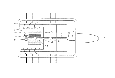
In Figure 1, "A" indicates a metal container, of the "flat pack" type,
which is to contain and to afford mechanical protection to the
assembly, as well as to act as an electromagnetic shield. An integrated
circuit B containing the laser driving circuit is located inside the
2 0 container. This integrated circuit is provided on its surface with a metal
ground area D on which a laser diode E is mounted. This is secured to
the ground area by means of an electrically conducting adhesive, for
example silver-charged epoxy resin, so that the driving current can flow
in the cathode. The ground area extends over the integrated circuit
2 5 surface by means of metallization strips C, which act as thermal
dissipation means for the laser.
The laser anode is connected by a bonding wire to a second metal
area N, connected to the driving circuit within the integrated circuit.
The light-emitting surface of the laser is faced by an optical fibre I
3 0 with pig tail functions. Fiber I can easily be positioned in
correspondence of the light-emitting surface thanks also to the help of a
central metallization strip M, deposited on the surface of the integrated
circuit and acting as a visual guide for the alignment.
The fibre is secured to the integrated circuit at a point F, to the
3 S metal container at a point L and to a fibre guiding device G at a point
H by epoxy resin gluing.
Since the laser is mounted directly on the surface of the integrated
circuit containing the driving circuit, as previously described, the
4 215904i
problems due to the length of the bonding wires and to the ~passage
through different connection sections realized with different techniques
are minimi~ed. A single, very short bonding wire is required between the
upper metallized surface of the laser and the metal area connected to
5 the output of the driving circuit.
Such mounting requires in any case good power dissipation,
lacking which the laser would undergo overheating, which would
compromise its correct operation. This thermal dissipation is
guaranteed by the aforesaid metallization strips.
Another important factor, from the point of view of thermal
balance, is constituted by the CMOS technology in which the driving
circuit is realized: as known, this technology is characterized by reduced
power consumption.
Figure 2 highlights how the fibre is horizontally aligned to the
15 emitting device thanks to a projecting portion P of the metal container,
whose thickness is equal to that of the integrated circuit. Point L for
securing the fibre, mentioned previously, is realized on this projecting
portion .
The existence of a fibre securing point directly on the integrated
2 0 circuit, near the laser diode, improves the efficiency and stability of the
optical coupling in the presence of temperature variations and of
mechanical stresses.
It is evident that what has been described is provided solely by way
of non-limiting example. Variations and modifications are possible
2 5 without departing from the scope of the invention.