Note: Descriptions are shown in the official language in which they were submitted.
2159129
1
OPTICAL CONTROL DEVICE AND METHOD FOR MAKING THE SAME
This invention relates to an optical control
device for switching light paths, modulating a light wave
and filtering a light wavelength, and more particularly to,
an optical control device of a waveguide-type in which the
control is carried out by using optical waveguides which are
formed on an electro-optic-effect crystalline substrate made
of lithium-containing material such as LiNb03, LiTa03 or
similar material, and to a method for making the same.
Along with the utilization of an optical
communication system, a large capacity and multi-function
system is desired. Also, enhanced functions such as high
speed generation of optical signals, high-speed switching of
an optical transmission line, and high-speed exchanging are
required.
As a means for switching optical transmission
lines and exchanges in a network, an optical switch is used.
The optical switch now available is operated by switching
light paths according to the mechanical movement of a prism,
mirror, fiber or the like. However, it has problems that
the operating speed is low and that it is too large to
construct a matrix switch. To overcome the problems, a
waveguide-type optical switch which employs optical
waveguides has been developed. It has advantages in that
high-speed operation, integration of numerous elements, and
high reliability can be realized. In particular, the
21591 29
2
optical switch which employs a ferroelectric material such
as lithium niobate(LiNb03) or the like has low light
absorption and high efficiency caused by the large electro-
optic effect. Various types of optical control devices are
reported, for example, a directional-coupler-type, mach-
zender-type, balance-bridge-type, total-reflection-type
optical switch.
Recently, the high-density integration of the
waveguide-type optical switch using a directional coupler
which is formed in an electro-optic-effect LiNb03 crystalline
substrate has been developed. H. Nishimoto (the inventor of
this application) et al., "Polarization Independent 8x8
LiNb03 Optical Matrix Switch", Electronic Information
Communication Society, OQE88-147, pp. 67-74 reports the 8x8
matrix optical switch in which 64 directional-coupler-type
optical switches is integrated in the LiNb03 crystalline
substrate. Also, a device such as an external optical
modulator which comprises a single optical switch has been
developed.
The characteristics concerning such waveguide-type
devices are stability in operation, switching voltage
(power), crosstalk, extinction ratio, loss, switching speed
and so on. The most important characteristic of these is
stability in operation.
However, the conventional optical control device
has a problem of DC drift which significantly affects
stability in operation and reliability of the device. The
2159129
3
DC drift is a phenomenon in which an optical-output to
applied-voltage characteristic shifts while a DC voltage is
continuously applied.
Accordingly, it is an object~of the invention to
provide an optical control device in which the DC drift can
be effectively suppressed to afford high reliability.
It is a further object of the invention to provide
a method for making an optical control device in which the
DC drift can be effectively suppressed to afford high
reliability.
In one form, the invention is an optical control
device that includes: a LiNb03 or LiTa03 crystalline sub-
strate having an electro-optic effect; a channel-type
optical waveguide which is formed in said crystalline
substrate by doping metal; an optically-transparent film
layer formed on said crystalline substrate; and electrodes
formed on said optically-trans-parent film layer. A portion
of a surface layer of the crystalline substrate is doped
with a metal, that portion extending on both sides of the
channel-type optical waveguide. Alternatively, an entire
surface layer of the crystalline substrate is doped with the
metal, including a part of the surface layer forming a
portion of the channel-type optical waveguide.
The channel-type optical waveguide may be formed
in said crystalline substrate by proton exchange rather than
by doping metal.
2159129
4
In the case where a portion of the surface layer
of the crystalline substrate is doped with a metal, the
metal for doping said channel-type optical waveguide or said
portion of the surface layer of the crystalline substrate is
selected from a group consisting of titanium, copper, vana-
dium, iron, molybdenum, chromium. In the case where an
entire surface layer of the crystalline substrate is doped
with a metal, the metal for doping said channel-type optical
waveguide or said entire surface layer of the crystalline
substrate is selected from a group consisting of titanium,
copper, vanadium, iron, molybdenum, chromium.
In the case where the channel-type optical wave-
guide is formed in the crystalline substrate by doping
metal, the crystalline substrate may be made of LiNb03, and
the channel-type optical waveguide may be formed by doping
titanium. In that case, where either the portion of the
surface layer of the crystalline substrate or the entire
surface of the crystalline substrate is doped with a metal,
that metal may be titanium.
In another form, the invention is a method for
making an optical control device, comprising the steps of:
preparing a LiNb03 crystalline substrate having an electro-
optic effect; thermally diffusing a metal into the crystal-
line substrate to form in the crystalline substrate a
channel-type waveguide; and, thermally diffusing the metal
into either a portion of the surface layer or the entire
21591 29
the surface layer in the thermal diffusion extends on both
sides of the channel-type optical waveguide being formed.
Thermal diffusion of the metal into the entire surface layer
of the crystalline substrate includes a part of the surface
5 layer that forms a portion of the channel-type optical wave-
guide being formed.
The thermal diffusion of a metal into the crystal-
line substrate to form a channel-type waveguide and the
thermal diffusion into a portion or the entire surface layer
l0 of the crystalline substrate are steps that may be performed
simultaneously, or they may be formed consecutively. In
either case, the channel-type optical waveguide and the
surface layer may be formed by doping titanium.
The invention will next be explained in more
detail in conjunction with the appended drawings, wherein:
Figure 1 is a cross-sectional view of a conven-
tional optical control device;
Figure 2 is a cross-sectional view of an optical
control device in a first preferred embodiment according to
the invention;
Figure 3 is a graph illustrating variation of the
amount of lithium mixed into a buffer layer depending on the
existence of a lithium blocking layer;
Figure 4 is a cross-sectional view of an optical
control device in a second preferred embodiment according to
the invention;
21591 29
6
Figure 5 is a cross-sectional view of an optical
control device in a third preferred embodiment according to
the invention;
Figures 6A and 6B are cross-sectional views of an
optical control device in a process for making an optical
control device according to the invention;
Figures 7A and 7B are cross-sectional views of an
optical control device in another process for making an
optical control device according to the invention;
Figure 8 is a cross-sectional view of an optical
control device in a fourth preferred embodiment according to
the invention;
Figure 9 is a cross-sectional view of an optical
control device in a fifth preferred embodiment according to
the invention;
Figure 10 is a cross-sectional view of an optical
control device in a sixth preferred embodiment according to
the invention;
Figures 11A to 11C are cross-sectional views of an
optical control device in a process for making the optical
control device in the fifth embodiment according to the
invention; and,
Figure 12 is a graph illustrating variation of the
amount of lithium mixed into a buffer layer depending on the
existence of a lithium blocking layer.
2159128 ~:
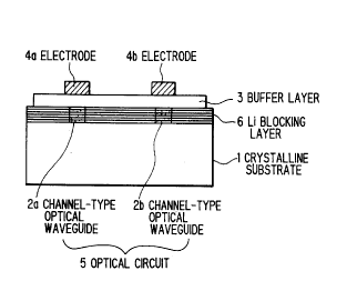
Before explaining an optical control device in the
preferred embodiment, the aforementioned conventional opti-
cal control device in Figure 1 will be explained.
As shown in Figure 1, the conventional optical
control device comprises an electro-optic crystalline sub-
strate 1 which is made of LiNb03, LiTa03 or like material,
and in which channel-type optical waveguides 2a and 2b form
a directional coupler 5. A buffer layer 3 is formed on the
electro-optic crystalline substrate 1, and metal electrodes
4a and 4b to which external control signals are applied
extend on buffer layer 3.
The buffer layer 3 of optically-transparent film
is used as an optical buffer layer to prevent the absorption
of the waveguided-light caused by the metal electrodes 4a
and 4b. It is generally made of Si02 since Si02 does not
absorb light and has a refractive index significantly less
than that of a LiNb03 or LiTa03 substrate. The electrodes 4a
and 4b generally employ a metal with low volume resistivity
so as to provide a high-speed operation, and are disposed
near the channel-type optical waveguides 2a and 2b.
The optical control devices of an optical wave-
guide-type having the above structure, such as an optical
switch or optical modulator, have been suggested. However,
they can not yet be put into practice since there is an open
question of DC drift which affects reliability of the
device. The DC drift is a phenomenon wherein an optical-
output to applied-voltage characteristic shifts while a DC
2159129
8
voltage is continuously applied. The DC drift is caused by
the impurity ions which are included in the buffer layer 3
which is deposited on the electro-optic crystalline sub-
strate 1 by the CVD or sputtering method. Namely, the
impurity ions may move according to the polarity thereof
under the electric field in the buffer layer 3 which is
generated by the voltage applied to the electrodes 4a and
4b. Due to the movement of ions, the anti-electric-field
which negates the electric field in the buffer layer 3 is
formed. This phenomenon is a cause of the DC drift. The
impurity ions contributory to the DC drift include sodium or
potassium which is naturally mixed, as well as lithium mixed
in the buffer layer 3 from the LiNb03 or LiTa03 substrate.
The mixing of lithium from the LiNb03 or LiTa03 substrate is
promoted by plasma or heat generated in the deposition by
the CVD or sputtering method.
Next, an optical control device in the first
preferred embodiment will be explained in Figure 2, wherein
like parts are indicated by like reference numerals as used
in Figure 1.
The optical control device in the first embodiment
is provided with an optical circuit 5 which has two channel-
type optical waveguides 2a and 2b, and electrodes 4a and 4b
which are formed on a buffer layer 3 of optically-trans-
parent film and are disposed over the channel-type optical
waveguides 2a and 2b. Herein, the optical circuit 5 may
employ a directional-coupler-type, mach-zender-type,
2159129
9
balance-bridge-type or a similar type. The buffer layer 3
is preferably made of Si02, but it also may be made of A1203,
MgF2, SiON, Si3N4 or similar material. The depositing of the
buffer layer 3 may be performed by the CVD method, sput-
tering method, vapor deposition method or similar method.
The electrodes 4a and 4b may be made of various conductive
materials, such as Au, A1, Mo, Cu, WSi, ITO, Zn0 or conduc-
tive polymer.
Further, in Figure 2, a metal-doped layer 6
(hereinafter referred to as "lithium blocking layer") is on
the entire surface of the LiNb03 crystalline substrate 1, as
well as on the surface of the channel-type optical wave-
guides 2a and 2b; the waveguides are made by doping metal
into parts of the surface of the LiNb03 crystalline substrate
1. The doping metal for forming the channel-type optical
waveguides 2a and 2b and lithium blocking layer 6 may in-
clude Ti, Cu, V, Fe, Mo, Cr or similar material. The doping
of metal may be performed by the thermal diffusion method,
ion implantation method or the like. Herein, the doping of
metal should be performed such that the refractive index of
the channel-type optical waveguides 2a and 2b is greater
than that of the lithium blocking layer 6.
Both the channel-type optical waveguides 2a and 2b
and lithium blocking layer 6 in the first embodiment are
formed by doping titanium by the thermal diffusion method.
Herein, the doping of titanium is performed such that the
21591 29
refractive index of the channel-type optical waveguides 2a
and 2b is greater than that of the lithium blocking layer 6.
In this embodiment, based on the refractive index increasing
with thickening of the titanium-deposited layer, the tita-
5 nium-deposited layer for the channel-type optical waveguides
2a and 2b is formed to be thicker than that for the lithium
blocking layer 6 to obtain a desired difference in refrac-
tive index. Namely, the titanium-deposited layer for the
channel-type optical waveguides 2a and 2b has a thickness of
10 0.05 to 0.15 nm, while the titanium-deposited layer for the
lithium blocking layer 6 has a thickness of between 1/100
and 4/5 the thickness of the titanium-deposited layer for
the channel-type optical waveguides 2a and 2b. Then, both
the titanium-deposited layers are processed by the thermal
diffusion at 850 to 1100°C for 0.5 to 20 hours to form the
channel-type optical waveguides 2a and 2b and lithium
blocking layer 6.
The inventor has found that lithium, which is a
component of the crystalline substrate 1, is mixed from the
LiNb03 or LiTa03 crystalline substrate 1 into the buffer
layer 3 of Si02 or the like due to plasma or heat when the
buffer layer 3 is deposited by CVD method, sputtering
method, vapor deposition method or the like. Furthermore,
he has found that the mixing of lithium is significantly
reduced at the region where the lithium blocking layer 6 is
formed as compared with at the region where the lithium
blocking layer 6 is not formed.
21591 29
11
Figure 3 shows variation of the amount of lithium
mixing into the Si02 buffer layer 3, depending on the exist-
ence of the lithium blocking layer 6; i.e., on the right end
point of the horizontal axis, the lithium blocking layer is
formed on the surface of the LiNb03 crystalline substrate 1;
on the left end point of the horizontal axis, the lithium
blocking layer is not formed on the surface of the LiNb03
crystalline substrate 1. The Si02 buffer layer 3 is formed by
the sputtering method. Due to the lithium blocking layer 6,
the amount of lithium mixing into the Si02 buffer layer is
reduced to about 1/50 the amount otherwise mixing.
Thus, according to the optical control device in
the first embodiment, the lithium mixing from the LiNb03
crystalline substrate 1 into the Si02 buffer layer 3 due to
plasma or heat when the Si02 buffer layer 3 is deposited by
CVD method, sputtering method, vapor deposition method or
similar method can be effectively reduced. Thereby, the DC
drift of the device can be suppressed to provide an optical
control device with high reliability.
Meanwhile, it will be easily appreciated that the
above optical control device can be obtained if only the
amount and depth of metal doped is set such that the chan-
nel-type optical waveguides 2a and 2b serve as a waveguide,
i.e., the amount, depth and type of metal doped are not
limited by the other condition.
With reference to Figure 4, an optical control
device in the second preferred embodiment will be explained.
21591 29
12
In this embodiment, an optical circuit 5 is a directional
coupler, and a lithium blocking layer 6 is formed on the
surface of a crystalline substrate 1 except in the region
where the waveguided-light propagates between channel-type
optical waveguides 2a and 2b. The lithium blocking layer 6
is not formed in the region between the channel-type optical
waveguides 2a and 2b of the directional coupler, since the
waveguided-light propagates therebetween. The second
embodiment can provide a similar advantage to that of the
first embodiment. In addition, the optical control device
in the second embodiment does not affect the propagation
characteristic of the waveguided-light through the channel-
type optical waveguides 2a and 2b. Therefore, reduction of
steps in processing and designing of the device, and a
higher yield, can be realized.
With reference to Figure 5, an optical control
device in the third preferred embodiment will be explained.
In this embodiment, channel-type optical waveguides 2a and
2b are formed on the surface of a LiTa03 crystalline sub-
strate 1 by proton exchanging, and a lithium blocking layer
6 is formed by doping metal on the entire surface of the
LiTa03 crystalline substrate 1. The proton exchanging that
forms the channel-type optical waveguides 2a and 2b may
employ benzoic acid, pyrophosphoric acid or the like. When
the crystalline substrate 1 is made of LiTa03, the lithium
blocking layer 6 is doped by ion implantation. When the
crystalline substrate 1 is made of LiNb03, the lithium
2159129
13
blocking layer 6 is doped by thermal diffusion or ion
implantation. The doping metal for forming the lithium
blocking layer 6 may include Ti, Cu, V, Fe, Mo, Cr or a
similar metal. The third embodiment can also provide a
similar advantage to that of the first embodiment.
Meanwhile, it will be easily appreciated that the
above optical control device can be obtained if only the
proton exchanging and the metal doping into the lithium
blocking layer 6 are performed such that the channel-type
optical waveguides 2a and 2b serve as a waveguide, i.e., the
amount and depth of the proton exchanging, and the amount,
depth and type of metal doped are not limited by the other
condition.
Figures 6A and 6B show the process for making an
optical control device in the first preferred embodiment
according to the invention.
First, on a LiNb03 crystalline substrate 1, a
patterned metal layer 7a for forming channel-type optical
waveguides 2a and 2b and a metal layer 7b for forming a
lithium blocking layer 6 are formed (Figure 6A). The
depositing of the metal layers 7a and 7b may be performed by
CVD, sputtering, vapor deposition method or the like. The
patterning of the metal layer 7a is by the standard litho-
graphy technique. Herein, the metal layer 7b for the
lithium blocking layer 6 may be patterned such that a region
is left for propagating waveguided-light without the lithium
blocking layer.
2159129
14
Next, by doping the metal in the metal layers 7a
and 7b into the LiNb03 crystalline substrate 1 by the thermal
diffusion, the channel-type optical waveguides 2a and 2b and
lithium blocking layer 6 are simultaneously formed (Figure
6B) .
Though the patterned metal layer 7a for forming
the channel-type optical waveguides 2a and 2b is mounted on
the metal layer 7b for forming the lithium blocking layer 6
in Figure 6A, it will be easily appreciated that the rela-
tionship in the mounting can be changed upside down, i.e.,
the metal layer 7b may be mounted on the metal layer 7a.
The doping metal may include Ti, Cu, V, Fe, Mo,
Cr, or similar metal. In this embodiment, both the channel
type optical waveguides 2a and 2b and lithium blocking layer
6 are formed by using titanium as the doping metal.
Figures 7A and 7B show the process for making an
optical control device in the second preferred embodiment
according to the invention. First, after depositing a metal
layer 7a for forming channel-type optical waveguides 2a and
2b as shown in Figure 6A on a LiNb03 crystalline substrate 1,
the metal layer 7a is processed by thermal diffusion to form
the channel-type optical waveguides 2a and 2b (Figure 7A).
Next, after depositing a metal layer 7b for forming a
lithium blocking layer 6 as shown in Figure 6A on the LiNb03
crystalline substrate 1, the metal layer 7b is processed by
thermal diffusion to form the lithium blocking layer 6
(Figure 7B) . Herein, the metal layer 7b for the lithium
2159129
blocking layer 6 may be patterned such that a region is left
for propagating waveguided-light without the lithium
blocking layer.
Similarly to the process in the first embodiment,
5 the depositing of the metal layers 7a and 7b may be per
formed by CVD, sputtering, vapor deposition method or
similar method. The patterning of the metal layer 7a is by
the standard lithography technique.
Though, in this embodiment, the lithium blocking
10 layer 6 is formed after the formation of the channel-type
optical waveguides 2a and 2b, the lithium blocking layer 6
can be formed before the formation of the channel-type
optical waveguides 2a and 2b.
Meanwhile, it will be easily appreciated that the
15 above optical control device can be obtained if only the
channel-type optical waveguides 2a and 2b serve as a wave
guide, i.e., the relationship in depth between the channel
type optical waveguides 2a and 2b and the lithium blocking
layer 6 is not limited by the other condition.
The doping metal may include Ti, Cu, V, Fe, Mo, Cr
or other similar metal. In this embodiment, both the
channel-type optical waveguides 2a and 2b and lithium
blocking layer 6 are formed by using titanium as the doping
metal.
With reference to Figure 8, an optical control
device in the fourth preferred embodiment will be explained.
21591 29
16
The optical control device in the fourth embodi-
ment is provided with an optical circuit 5 which has two
channel-type optical waveguides 2a and 2b which are formed
on a LiNb03 crystalline substrate 1 by the thermal diffusion
method, and electrodes 4a and 4b which are formed on a buf-
fer layer 3 of optically-transparent film and are disposed
over the channel-type optical waveguides 2a and 2b. Herein,
the optical circuit 5 may employ a directional-coupler-type,
mach-zender-type, balance-bridge-type or similar type. The
buffer layer 3 is preferably made of Si02, and it also may
be made of A1203, MgF2, SiON, Si3N4 or like material. The
depositing of the buffer layer 3 may be performed by the CVD
method, sputtering method, vapor deposition method or simi-
lar method. The electrodes 4a and 4b may be made of various
conductive materials, such as Au, A1, Mo, Cu, WSi, ITO, Zn0
or conductive polymer.
Between the LiNb03 crystalline substrate 1 and the
buffer layer 3, a film layer 6 (hereinafter referred to as
"lithium blocking layer") which is separated from the buffer
layer 3 is provided. Herein, the lithium blocking layer 6
is not formed in the region for propagating waveguided-
light. Thus, when the optical circuit 5 employs a direc-
tional coupler or X-type, the lithium blocking layer 6, as
shown in Figure 8, is not formed on the channel-type optical
waveguides 2a and 2b nor between the channel-type optical
waveguides 2a and 2b.
21591 29
17
The lithium blocking layer 6 may be made of a
metal or semiconductor material of a single element in-
cluding Si, Ti, Cu, V, Fe, Mo, Cr or similar material, or a
dielectric, metal, semiconductor, organic material or
similar material in which is difficult to generate ionic
polarization by applying an electric field, such as crystal
doped by phosphorus, MgF2, Si3N4, WSi, GaAs, Inp, polyimide.
The substrate 1 is limited to the LiNb03 crystal-
line substrate, and any lithium-containing crystalline sub-
strate such as a LiTa03 crystalline substrate may be used.
The depositing of the lithium blocking layer 6 may
be performed by CVD, sputtering, vapor deposition method or
similar method. The standard lithography technique is
employed to preclude the formation of the lithium blocking
layer at the region for propagating waveguided-light.
A titanium-deposited layer with a thickness of
0.02 to 0.15 nm is processed by the thermal diffusion at 850
to 1100°C for 0.5 to 20 hours to form the channel-type
optical waveguides 2a and 2b.
With reference to Figure 9, an optical control
device in the fifth preferred embodiment will be explained.
In this embodiment, on the intermediate step in
the process for making the optical control device, a lithium
blocking layer 6 and buffer layer 3 between two channel-type
optical waveguides 2a and 2b is partially removed. This
structure is suitable for the case that the lithium blocking
layer 6 between the channel-type optical waveguides 2a and
21591 29
18
2b is not proper, i.e., when the optical circuit 5 is a
directional coupler, X-type or the like. Because the
covering area of the lithium blocking layer 6 is greater
than that of the lithium blocking layer 6 in the fourth
embodiment, the lithium mixing into the buffer layer 3 when
the buffer layer 3 is deposited can be further reduced to
further suppress the DC drift and provide an optical control
device with higher reliability.
With reference to Figure 10, an optical control
device in the sixth preferred embodiment will be explained.
This embodiment is suitable for the case in which
waveguided-light in optical circuit 5 does not propagate
between two channel-type optical waveguides 2a and 2b, such
as when a mach-zender-type, balance-bridge-type is employed.
Namely, a lithium blocking layer 6 is also formed between
the channel-type optical waveguides 2a and 2b. Because the
covering area of the lithium blocking layer 6 is greater
than that of the lithium blocking layer 6 in the fourth
embodiment, the lithium mixing into the buffer layer 3 when
the buffer layer 3 is deposited can be further reduced to
further suppress the DC drift and provide an optical control
device with higher reliability.
Figures 11A to 11C show the process for making the
optical device in the fifth embodiment.
First, as shown in Figure ilA, after forming the
directional coupler 5 of the channel-type optical waveguides
2a and 2b on the LiNb03 crystalline substrate 1 by the ther-
21591 29
19
mal diffusion of titanium, the lithium blocking layer 6 is
deposited on the LiNb03 crystalline substrate 1, except on
the channel-type optical waveguides 2a and 2b. In this
embodiment, the lithium blocking layer 6 is deposited with
chromium by electron-beam vapor deposition, thermal deposi-
tion, sputtering method or similar method. Thereafter, the
lithium blocking layer 6 corresponding to the region where
the electrodes 4a and 4b will be provided is removed by
using the standard photolithography technique and etching.
Next, as shown in Figure 11B, Si02 is deposited
thereon to form a buffer layer 3, by CVD, a sputtering
method or a similar method. Optionally, the buffer layer 3
may be annealed. Thereafter, the lithium blocking layer 6
and buffer layer 3 between the channel-type optical wave-
guides 2a and 2b are removed by using the standard photo-
lithography technique and etching.
Finally, as shown in Figure 11C, the layer for
forming the electrodes 4a and 4b is deposited by electron-
beam vapor deposition, thermal vapor deposition, sputtering
method or similar method, thereafter forming the electrodes
4a and 4b by using the standard photolithography technique
and etching. The electrodes are mainly made of gold.
Alternatively, the removing of the lithium
blocking layer 6 and buffer layer 3 between the channel-type
optical waveguides 2a and 2b as in Figure 11B may be simul-
taneously carried out after the forming of the electrodes 4a
and 4b.
~t,.a.
i
21591 29
From the above-mentioned process, the process for
making the optical control devices in the fourth and sixth
embodiments will be easily understood. Namely, after
forming the directional coupler 5 of two waveguides 2a and
5 2b on the LiNb03 crystalline substrate 1 by the thermal
diffusion, the layer for forming the lithium blocking layer
6 is deposited. Thereafter, the lithium blocking layer 6
corresponding to the region where the electrodes 4a and 4b
will be formed, or the lithium blocking layer 6 corres-
10 ponding to the above-mentioned region and the region between
the electrodes 4a and 4b, is removed. Thereafter, the buf-
fer layer 3 is deposited thereon. Finally, similarly to the
fifth embodiment, the electrodes 4a and 4b are formed on the
buffer layer 3.
15 Figure 12 shows an amount of lithium mixing into
the Si02 buffer layer 3, depending on the existence of the
lithium blocking layer 6, i.e., on the right end point of
the horizontal axis, the lithium blocking layer is formed on
the surface of the LiNb03 crystalline substrate 1 (in the
20 fourth to sixth embodiments); on the left end point of the
horizontal axis, the lithium blocking layer is not formed on
the surface of the LiNb03 crystalline substrate 1. The Si02
buffer layer 3 is formed by the sputtering method. Due to
the lithium blocking layer 6, the amount of lithium mixture
2 5 into the S i02 buf f er layer 3 i s reduced to about 1 / 5 0 the
amount otherwise.
2159129
21
Thus, according to the optical control device, the
lithium mixing from the LiNb03 crystalline substrate 1 into
the Si02 buffer layer 3 due to plasma or heat when the Si02
buffer layer 3 is deposited by CVD method, sputtering
method, vapor deposition method or similar method can be
effectively reduced.
Although the invention has been described with
respect to specific embodiment for complete and clear
disclosure, the appended claims are not to be thus limited
but are to be construed as embodying all modifications and
alternative constructions that may occur to one skilled in
the art and which fairly fall within the basic teaching
herein set forth.