Note: Descriptions are shown in the official language in which they were submitted.
CA 02159242 1999-OS-20
1
PROCESS FOR MANUFACTURING SEMICONDUCTOR DEVICE
AND SEMICONDUCTOR WAFER
The present invention relates to a process for
manufacturing a semiconductor device and, more particular-
ly, to a process suited for mass production of a highly-
integrated semiconductor device.
Semiconductor devices of various forms have been
developed to meet recent demands in the electronics field
towards reduced size and weight, increased speed, and
improved functional operation. The semiconductor device
comprises a package and a semiconductor chip (hereinafter,
also referred to as a chip) contained in the package. The
higher the level of chip integration, the greater the
number of terminals required thereon. In addition, there
are demands for further reductions in the size of semicon-
ductor chips. The terminal-to-terminal pitch must be
reduced to meet the demands for smaller semiconductor
devices. A semiconductor device having a high terminal
count can be obtained by inner lead bonding or by area
array bonding. Inner lead bonding and area array bonding
are expected to become standard techniques in the field of
semiconductors.
Inner lead bonding (ILB) is used to make elec-
trical contact between the chip and the leads within the
package. Various bonding technologies are available to
achieve this inner lead bonding. Wire bonding is the most
CA 02159242 1999-OS-20
2
extensively used electrical interconnection process. In
this process, fine wires are used to make electrical
contact between the bonding pads on the chip and the
corresponding leads on the package. the wire diameter is
typically from 20 to 30 micrometers. Wire bonding tech-
niques include thermocompression bonding, ultrasonic
bonding, and thermosonic bonding.
The use of the fine wires limits the number of
interconnections available in one package. Recent demands
for semiconductor devices with a high terminal count thus
cause a problem of poor connections between the wire and
the bonding pads. Considering this fact, wire bonding has
been replaced with wireless bonding. Wireless bonding is
also called gang bonding, with which bumps formed on the
electrode pads are bonded simultaneously to the leads.
Wireless bonding techniques include tape automated bonding
(TAB) and flip-chip bonding. TAB is also referred to as
tape carrier bonding.
In the TAB technique, a laminated tape of gold-
plated copper foil etched in the form of a lead is bonded
to the bumps on the electrode pads. The elimination of
wire bonding is advantageous from viewpoints of size
reduction and highly integrated packaging of the device.
On the other hand, the flip-chip bonding requires a raised
metallic bump of solder on the chip. The chip is then
inverted and bonded face down to the substrate intercon-
nection pattern. This process lends itself to production
CA 02159242 1999-OS-20
3
of semiconductor devices with a high terminal count and a
smaller pitch. In addition, this technique is also advan-
tageous to provide a fast, low-noise semiconductor device
owing to the short length of the interconnections.
The TAB and flip-chip bonding techniques use the
bumps provided between the chip and the package to make
electrical interconnection between them. These techniques
are disclosed in, for example, Japanese patent Laid-open
Nos. 5-129366 and 6-77293.
A film carrier semiconductor device disclosed in
these laid-open patent publications uses the bumps for the
electrical interconnection between the chip and the car-
rier film. There is another film carrier semiconductor
device in which the electrical interconnection between the
chip and the carrier film is achieved without using the
bumps. The semiconductor chip and the carrier film are
electrically connected during the assembly process. The
bumps are used only for the purpose of connecting the film
carrier semiconductor device with, for example, a circuit
board or a mounting board. The film carrier semiconductor
device of the type described comprises a semiconductor
chip and a carrier film. Contact pads are provided along
the periphery of one side of the semi-conductor chip.
Interconnecting layers are provided on the carrier film.
The carrier film is also provided with through-holes and
openings formed therein. The openings are formed at the
CA 02159242 1999-OS-20
4
position corresponding to the contact pads (chip elec-
trodes).
A conventional process for manufacturing a
semiconductor device is described first for the purpose of
facilitating the understanding of the present invention.
In particular, a process for manufacturing a film carrier
semiconductor device is described. A wafer, which com-
prises a number of chip sections each having chip elec-
trodes formed thereon, is covered with a passivating film
using a well-known technique. After the formation of the
passivating film, the chip electrodes are exposed to the
atmosphere. The chip sections are then separated from
each other into individual chips along scribe lines by
means of a known dicing technique using a dicing saw. The
semiconductor chip so obtained is prepared along with a
carrier film and an adhesion film. The adhesion film is
positioned relative to the semiconductor chip and placed
thereon. The carrier film and the semiconductor chip are
subjected to heat and pressure to adhere them through the
adhesion film. The carrier film is then cut along the
edges of the chip by means of a standard method. Next,
bump electrodes (solder bumps) are formed on corresponding
outer chip electrodes arranged on the carrier film.
Semiconductor devices so obtained may find
various applications in the electronics, electrical, and
other fields. For example, semiconductor devices may be
used for memories and drivers for a liquid crystal dis-
CA 02159242 1999-OS-20
play. Such applications are suited for mass-production of
the semiconductor device. However, the above mentioned
manufacturing process limits the number of chips obtained
per unit time because the operation is made for each chip.
5 Recent demands for smaller-sized memories or drivers have
reduced the size of the semiconductor device itself.
Accordingly, operations such as the inner lead bonding and
the formation of the bumps must be conducted for each
small chip. This operation is intricate and somewhat
troublesome because the semiconductor chip is relatively
small. It is thus difficult to position the carrier film
positively or with a high accuracy. The intricacy is also
associated with reduced reliability of the electrical
interconnection between the semiconductor chip and the
carrier film. In other words, there may be trouble in the
interconnection between the semiconductor chip and the
carrier film as well as in the adhesion of the individual
components. With this respect, a batch process may be
more effective than the conventional process for mass-
production of semiconductor devices, in which most opera-
tions are conducted on chip sections of a wafer. In this
process, the bump electrodes are formed on the chip
sections of the wafer prior to separation into individual
chips.
Such a method is disclosed in, for example, U.S.
Patent No. 5,137,845, issued to Lochon et al. This method
was developed by IBM Corporation and is applicable to the
CA 02159242 1999-OS-20
6
manufacture of bump electrodes for semiconductor chips
that are suitable for Controlled Collapse Chip Connection
(C4) or flip-chip technique. In this method, a barrier
metal is deposited on aluminum chip electrodes, on which
bump electrodes are deposited for a terminal contact. The
method is, however, directed to the whole wafer as such.
In other words, this patent is not for a wafer to be
divided into semiconductor chips. Neither the separation
of the wafer nor the position of the interconnection, chip
electrodes, and bump electrodes to avoid breakage of them
upon dicing are disclosed. In addition, the bump elec-
trodes in the above mentioned conventional semiconductor
devices are formed on the chip electrodes. The formation
of the bumps on the electrodes is, however, difficult or
impossible if the demands for reduced size, a higher ter-
urinal count, and a smaller pitch are to be met.
This problem may be solved by using a multi-
layered electrode structure for the semiconductor device
which allows for the distribution of solder pads over the
entire surface of the semiconductor chip. Such a struc-
ture is, however, complex and difficult to manufacture.
In addition, the multi-layered electrode significantly
affects the configuration of the chip surface. A larger
number of layers may sometimes make the surface irregular.
An object of the present invention is to provide
a process for manufacturing a semiconductor device having
CA 02159242 1999-OS-20
7
bump electrodes formed at different positions from chip
electrodes, which is suited for mass-production.
Another object of the present invention is to
provide a process for manufacturing a semiconductor device
having good thermal stress resistance.
Yet another object of the present invention is
to provide a process for manufacturing a semiconductor
device having good moisture resistance.
In order to achieve the above mentioned object,
there is provided a process for manufacturing a semi-
conductor device comprising the steps of defining a number
of semiconductor chip sections on a wafer, each semi-
conductor chip section having a number of chip electrodes
formed on one surface along a periphery thereof, the one
surface being covered with a passivating film except for
the positions where the chip electrodes are formed;
forming a number of interconnection layers on the wafer
for each semiconductor chip section such that each inter-
connection layer is connected to the chip electrode at one
end thereof and is extended inward the chip section at the
other end; covering the entire surface of the wafer with a
cover coating film; forming a number of apertures in the
cover coating film, the apertures being formed into a
matrix; forming a number of bumps on the apertures; and
separating the semiconductor chip sections along scribe
lines on the wafer into individual semi-conductor chips.
CA 02159242 1999-OS-20
8
In the above mentioned process, the interconnec-
tion layer extended inward the semiconductor chip section
is preferably exposed to the atmosphere through apertures
in the cover coating film. In addition, the solder bumps
are preferably formed away from the scribe line. Further-
more, the bump electrodes are preferably formed at a
position not directly over the chip electrodes.
According to another aspect of the present
invention, there is provided a semiconductor wafer having
a number of semiconductor chips comprising bump electrodes
formed into a matrix on an entire surface of the wafer ex-
cept for on scribe lines between the semiconductor chips.
The invention will now be described, by way of
example, with reference to the accompanying drawings in
which like reference numerals refer to like parts and
components and in which:
Figure lA is a schematic plan view of a wafer
having a number of chip sections subjected to a conven-
tional process for manufacturing a semiconductor device;
Figure 1B is an enlarged view of a chip section
in Figure lA;
Figure iC is a cross-sectional view of the chip
section taken on line I-I in Figure 1B;
Figures 2A through 2G are cross-sectional flow
diagrams showing a process for manufacturing a conven-
tional semiconductor device;
CA 02159242 1999-OS-20
9
Figures 3A through 3G are cross-sectional flow
diagrams showing a process for manufacturing a semicon-
ductor device according to an embodiment of the present
invention;
Figure 4A is a schematic plan view of a wafer
having a number of chip sections according to a process
for manufacturing a semiconductor device of the present
invention;
Figure 4B is an enlarged view of a chip section
in Figure 4A; and
Figure 4C is a cross-sectional view of the chip
section taken on line II-II in Figure 4B.
A conventional process for manufacturing a semi-
conductor device is described first for the purpose of
facilitating the understanding of the present invention.
In particular, a process for manufacturing a film carrier
semiconductor device is described. Referring to Figures
lA through 1C, a semiconductor chip is prepared by using,
for example, a well-known wafer manufacturing technique.
A wafer 10' comprises a number of chip sections 10a' each
having chip electrodes (contact pads) 11 formed thereon.
Though the illustrated chip electrodes 11 are formed along
the periphery of each chip section l0a', the chip elec-
trodes may be formed within an active area. The chip
electrodes 11 are typically made of an aluminum-based
alloy. The wafer 10' is then provided with a passivating
film 12. More particularly, the entire surface of the
CA 02159242 1999-OS-20
wafer 10' is covered with the passivating film 12. The
passivating film 12 may be made of, for example, polyi-
mide, silicon nitride, or silicon oxide by using a well-
known technique such as spin coating. The passivating
5 film 12 may be made of, for example, polyimide, silicon
nitride, or silicon oxide by using a well-known technique
such as spin coating. The passivating film has a thick-
ness of 20 micrometers or less. After formation of the
passivating film, the chip electrodes 11 are exposed to
10 the atmosphere by means of exposing the wafer 10' to light
and etching it. As a result, the passivating film 12
covers the entire surface of the wafer 10' except for the
locations where the chip electrodes 11 are formed. The
chip sections 10a' are then separated from each other into
individual chips along scribe lines 13. The separation is
made by means of a known dicing technique using a dicing
saw.
Referring to Figure 2, a process for manufac-
turfing a conventional semiconductor device is described.
A semiconductor chip 20 obtained in the manner described
above is prepared along with an adhesion film 25 and a
carrier film 30 (Figure 2A). Ball bumps 14 of gold are
formed on the chip electrodes 11. The adhesion film 25 is
interposed between the semiconductor chip 20 and the car-
rier film 30. The adhesion film 25 is smaller than the
semiconductor chip 20 and has a thickness of about several
tens of micrometers.
CA 02159242 1999-OS-20
11
The carrier film 30 comprises an organic insula-
tion film 31. The organic insulation film 31 may be, for
example, a polyimide-based insulation film. The organic
insulation film 31 has a first surface 31a and a second
surface 31b. Interconnection layers 32 are pro-vided on
the organic insulation film 31 on the side of the first
surface 31a. Through-holes 33 are formed in the insula-
tion film 31. One end of each through-hole 33 faces the
interconnection layer 32. Each through-hole 33 passes
through the insulation film 31 to the second surface 31b
thereof. The insulation film 31 is also provided with
openings 34 penetrating through the film. The openings 34
are formed at the position corresponding to the chip elec-
trodes 21. Each through-hole 33 is filled with a conduc-
tive electrode 35. Likewise, each opening 34 is filled
with a filler material 36.
Referring to Figure 2B, the adhesion film 25 is
positioned relative to the semiconductor chip 20 and
placed thereon. When made of a thermoplastic resin, the
adhesion film 25 can be temporarily fixed on the semi-
conductor chip 20 by means of heating it from the side of
the chip up to a temperature at which the adhesion film 25
begins to melt. In this event, the adhesion film 25 is
adhered to the semiconductor chip 20 in such a manner that
no voids are trapped between the film 25 and the chip 20.
Referring to Figure 2C, the carrier film 30 is
positioned relative to the semiconductor chip 20 with the
CA 02159242 1999-OS-20
12
adhesion film 25 thereon, and the interconnection layers
32 are connected to the chip electrodes 11 via the ball
bumps 14 by means of the inner lead bonding technique.
More specifically, the conductive electrode 35 contacts
with one end of the interconnection layer 32. The other
end of the inter-connection layer 32 reaches between the
contact pad 11 and the opening 34. In this event, the
aluminum forming the chip electrode 11 is reacted with
copper forming the interconnection layer 32 and with the
gold forming the ball bumps 14 into an aluminum-copper-
gold alloy to ensure the interconnection between them.
Referring to Figure 2D, the combination of the
semiconductor chip 20 and the carrier film 30 is subjected
to heat and pressure to adhere them via the adhesion film
25. The combination, which is referred hereinafter to as
a chip assembly, is heated and pressurized for several
seconds from the side of either the semiconductor chip 20
or the carrier film 30.
The above mentioned steps illustrated in Figures
2B through 2D are not a limitation on the method available
for connecting the carrier film 30 and the semiconductor
chip 20. The adhesion film 25 may be positioned and plated
relative to the carrier film 30 rather than the semicon-
ductor chip 20. Alternatively, the inner lead bonding may
be performed with high accuracy after the carrier film 30
is adhered to the semiconductor chip 20 with the adhesion
film 25 interposed between them. Further, an adhesion
CA 02159242 1999-OS-20
13
layer may be formed previously on the surface of the chip
section of the wafer.
In Figure 2E, the chip assembly is subjected to
an electrical sorting operation and tests for long-term
reliability under low electric field bias temperature (BT)
are performed using a sorting pad 50 in the same manner as
in typical tape carrier packages (TCP). The outer
configuration and dimensions of the carrier film 30 are
designed to meet the specifications determined by Elec-
tronic Industries Association of Japan (EIAJ). Such a
design allows common use of sorting tools such as sockets
and balls for various semiconductor devices.
In Figure 2F, product names are labelled on the
back surface of the chip using a laser beam. The carrier
film 30 is then cut along the edges of the chip assembly
using a mold. Typically, the cutting length and width are
larger by approximately 100 micrometers on each side than
those of the chip assembly when a mold is not used for
cutting. More precise cutting may be achieved using a
dicing saw or a laser beam.
Referring to Figure 2G, bump electrodes (solder
bumps) 37 are formed on corresponding outer chip elec-
trodes 11 arranged as an array on the carrier film 30 at
the second surface 31b thereof. The bump electrodes 37
may be formed using a method disclosed in, for example,
Japanese Patent Laid-open No. 49-52973. The bump elec-
trodes 37 are formed by soldering a wire using the wire
CA 02159242 1999-OS-20
14
bonding process on the surfaces of the chip assembly
corresponding to the chip electrodes 11 on the semicon-
ductor chip. The balls are then bonded to the pads,
following which the wires are cut.
As mentioned above, this conventional manu-
facturing process is practical only for a limited number
of chips obtained per unit time because it is necessary to
conduct operations such as inner lead bonding and form-
ation of the bumps for each small chip independently.
Accordingly, there may be a problem in the interconnection
between the semiconductor chip and the carrier film as
well as in the adhesion of the individual components. In
addition, the bump electrodes in the above mentioned con-
ventional semiconductor devices are formed on the corres-
ponding chip electrodes, which makes it difficult to meet
the demands of reduced size, a higher terminal count, and
a smaller pitch.
Next, an embodiment of the present invention is
described with reference to Figures 3A through 3G and 4A
through 4C. As shown in Figure 3A, a number of semi-
conductor chip sections l0a are defined on a wafer 10
according to a well-known wafer manufacturing process.
The chip section in this embodiment is square but may be
rectangular for other applications. Each semiconductor
chip section l0a has a number of chip electrodes (contact
pads) 11 formed on one surface along the periphery
thereof. Referring to Figure 3B, the wafer 10 is covered
CA 02159242 1999-OS-20
with a passivating film 12 having a thickness of 20
micrometers or less. The passivating film 12 may be
formed by means of any one of standard methods such as
spin coating. In this event, the passivating film 12
5 covers the entire surface of the wafer 10 including the
chip sections defined by scribe lines 13 with the chip
electrodes il thereon. The wafer 10 is then subjected to
well-known exposure and etching procedures to expose the
chip electrodes 11 to the atmosphere. This is clearly
10 shown in Figure 3B. The wafer 10 at this stage is similar
to the wafer 10' illustrated in Figure 1C. As mentioned
above, the conventional manufacturing process then divides
the wafer into the semiconductor chips along the scribe
line 13. In contrast, no dicing is made at this stage in
15 the present invention.
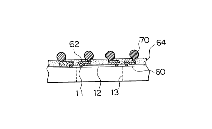
Referring to Figure 3C, aluminum interconnection
layers 60 are formed on the wafer 10. The aluminum
interconnection layer 60 has a thickness of 1 micrometer
or less and is connected to the chip electrode 11 at one
end thereof. The other end of the aluminum interconnec-
tion layer 60 is extended inward on the chip section 10a.
In other words, the aluminum interconnection layer 60 is
extended towards the central portion of the chip section
10a. The aluminum interconnection layer 60 may be formed
by means of a thin-film deposition technique such as
sputtering using a mask. Referring to Figure 3D, a nickel
plating 62 is made on the aluminum inter-connection layer
CA 02159242 1999-OS-20
16
60. The nickel plating has a thickness of at least 5
micrometers in order to absorb any thermal stress gener-
ated due to the difference in coefficient of thermal
expansion between the final semiconductor device and a
circuit board on which the semiconductor device is to be
mounted. The thickness of the nickel plating 62 also
affects on the reliability of the joint between the nickel
surface and a bump electrode formed later. In this
embodiment, the nickel plating has the thickness of 10
micrometers. The plating on the aluminum interconnection
layer 60 is not limited to nickel, and other metals such
as copper may be used, provided that they have the desired
adhesion and diffusion barrier properties, for compatibi-
lity with the material of the bump electrodes (solder in
this embodiment).
Referring to Figure 3E, a cover coating film 64
is applied on the nickel plating 62 and the passivating
film 12. The cover coating film 64 may be made of, for
example, polyimide applied to have a thickness of 20
micrometers or less. This cover coating film 64 is
similar in function to the organic insulation film 31 of
the carrier film 30 described in conjunction with the
conventional process. Next, a number of apertures 66 are
formed in the cover coating film 64. The position of the
apertures 66 corresponds to where the bump electrodes
described below are formed. Accordingly, the position of
the apertures 66 is not limited to a specific embodiment
CA 02159242 1999-OS-20
17
and may be selected depending on the application of the
resultant semiconductor device. The aperture 66 is formed
by means of, for example, etching or laser to the extent
that the surface of the nickel plating 62 is exposed to
the atmosphere. Subsequently, a gold plating 68 is made
on the exposed surface of the nickel plating 62. Though
not necessary, the gold plating 68 is preferable for
higher reliability of the bump electrodes.
Referring to Figure 3F, bump electrodes 70 are
formed in the aperture 68 and on the surface of the cover
coating film 64. The bump electrode 70 may be generally
spherical or hemispherical and about 100 micrometers high,
but different shapes may be used. The bump electrode 70
may be made according to the following steps. A solder
piece is cut from a solder strip using a die and a punch.
This solder piece is adhered in the aperture 66 using an
adhesive material such as rosin (flux). The solder piece
is then heated and melted to form the bump electrode. The
rosin is washed out after the formation of the bump elec-
trodes 70.
The wafer at this stage is illustrated in
Figures 4A through 4C. As apparent from the figures, the
bump electrodes 70 are formed on the entire surface of the
wafer 10 except for where the scribe lines are defined. In
addition, the aluminum interconnection layer 60 is ex-
tended to the position of the aperture 66. Though the
bump electrodes 70 in this embodiment are formed on the
CA 02159242 1999-OS-20
18
entire surface of the wafer except for the portions just
under which the chip electrodes 11 are formed, the bumps
70 may also be formed over the chip electrodes 11.
Turning to Figure 3G, the semiconductor chip
sections defined on the wafer 10 are separated from each
other into individual semiconductor devices 80 by means of
dicing.
The conventional wafer 10' illustrated in Figure
1A has the chip electrodes 11 separated from each other at
a pitch of approximately 0.1 mm. The resultant semicon-
ductor device thus has the bump electrodes away from each
other at the same pitch of 0.1 mm or less. In contrast,
the pitch can be increased up to approximately 0.5 mm
between the bump electrodes 70 on the semiconductor device
80 of the present invention. Accordingly, fusion or
melting of adjacent bumps can be reduced significantly
which otherwise may occur during the formation of the bump
electrodes. In addition, the semiconductor device
according to the present invention can be mounted on, for
example, a circuit board, with a higher yield. Further
more, the present process provides easier standardization
of semiconductor devices. This process also provides a
higher reliability of the joint between the bump elec-
trodes and the nickel or gold plating.
As mentioned above, the present invention makes
it possible to mass-produce semiconductor devices without
making a large investment in manufacturing facilities
CA 02159242 1999-OS-20
19
because the present process is compatible with a well-
known chip manufacturing process. The semiconductor
device obtained according to the present invention has a
superior thermal stress resistance and reliable joints
between the adjacent layers. This improves the moisture
resistance of the semiconductor device.
While the present invention has thus been des-
cribed in conjunction with a specific embodiment thereof,
it is understood that the present invention is not limited
to the illustrated embodiment. Instead, any changes,
modifications, and variations may be made by those skilled
in the art without departing from the scope and spirit of
the appended claims. For example, gold may be used for
the bumps rather than the solder. In such a case, the
nickel plating and the gold plating can be eliminated.