Note: Descriptions are shown in the official language in which they were submitted.
CA 02159243 1998-11-30
METHOD OF MANUFACTURING CHIP-SIZE
PACKAGE-TYPE SEMICONDUCTOR DEVICE
The present invention relates to a method of
manufacturing a semiconductor device, and more
specifically, to a method of manufacturing a
semiconductor device, called a chip-size package, which
is suitable for high-density packaging.
Various types of semiconductor devices have been
developed for satisfying demands for electronic devices,
such as, reduction in size and weight, speed-up and multi-
functionalization thereof. Demands for increasing the
number of pins due to the high integration of the
semiconductor chips and for reduction in size and
thickness of the semiconductor devices have been getting
stronger so that the fine-pitch arrangement of the pins
is essential for satisfying both demands. Thus, it is
considered that the inner-lead connection which can
narrow pitches of the pins and the area-array connection
which can enlarge pitches of the pins are the essential
techniques.
CA 02159243 1998-11-30
2
A chip-size package-type semiconductor device
is in the form of a semiconductor chip and a carrier
film which are integrally bonded by means of an adhesive
film. One side of the semiconductor chip, which is
attached to the carrier film, is formed with a plurality
of electrode pads along the edge thereof. The
carrier film includes an organic insulating film and
wiring layers formed on the organic insulating fi: ~.
Each of the wiring layers includes a region for
connection to the corresponding electrode pad of the
semiconductor chip. Further, a plurality of bump
electrodes are formed as electrode pads of the carrier
film for connection to the exterior. The bump electrodes
are arranged in a grid at regular pitches and distributed
widely on a side of the organic insulating film remote
from the wiring layers. The wiring layers are provided
on a surface of the carrier film facing the semiconductor
chip. Each of the wiring layers has one end connected to
the corresponding bump electrode through a via hole which
is formed by using a metal material to fill a through hole
formed at the organic insulating film. Other through
holes are further formed at the carrier film, and the
metal material is used to fill these other through holes
so as to form via holes, each for connection between the
wiring layer and the electrode pad as inner leads. Each
via hole is adjustable in position, when formed, relative
to the electrode pad and the wiring layer. The inner-
lead connection of the electrode pad and the Wiring layer
CA 02159243 1998-11-30
3
is achieved through this via hole.
The chip-size package-type semiconductor device
is, in general, manufactured in the following manner:
After temporarily attaching the adhesive film to
either one of the semiconductor chip and the carrier
film, the electrode pads and the wiring layers are
electrically connected to each other. Subsequently, the
adhesive film is bonded to the other of the semiconductor
chip and the carrier film by applying heat and pressure.
Thus, the size of the adhesive film is limited to the size
corresponding to an area defined within the electrode
pads, that is, not corresponding to all the area of the
joint surface of the semiconductor chip, so as to avoid
overlapping the electrode pads.
However, in such a manufacturing method, setting or
positioning of the adhesive film relative to the
semiconductor chip is difficult. Further, since the
adhesive film is not interposed between the semiconductor
chip and the carrier film at regions along the edge of
the semiconductor chip, sealing therebetween tends to be
insufficient. When the sealing is insufficient, protection
from moisture is reduced; thus leading to insulation
failure and further to reduction in service life of the
semiconductor device.
Further, in this kind of the chip-size package-
type semiconductor device, it is important that the
diameter of each of the through holes formed at the
organic insulating film be set as small as possible for
CA 02159243 1998-11-30
4
rendering a pitch of the bump electrodes 24 as small as
possible. In general, the through hole is formed by the
chemical etching or the laser processing using the
excimer (KrF) laser. The excimer laser is used because
it is difficult to achieve the fine processing using the
well-known YAG laser. However, it is also difficult to
achieve the fine processing even using the chemical
etching, and further, although the excimer laser can
achieve the fine processing, its oscillating tube is
expensive and its maintenance cost is high.
Under these circumstances, in the conventional
processing method, the minimum diameter of the through
hole is SO a m. Further, the shape of the through hole
is tapered. Thus, narrowing of the pitches of the
through holes is limited.
It is an object of the present invention to
provide a method of manufacturing a semiconductor device
which can reliably achieve sealing at a joint portion
between a semiconductor chip and a carrier film.
It is another object of the present invention to
provide a method of manufacturing a semiconductor device
which can ensure electrical connection between an
electrode pad of a semiconductor chip and a wiring layer
of a carrier film so as to improve durability of the
device.
CA 02159243 1998-11-30
It is another object of the present invention to
provide a method of manufacturing a semiconductor device
which can easily realize, at a low cost, a bump electrode
necessary for a carrier film for connection to the
exterior.
It is another object of the present invention to
provide a method of manufacturing a semiconductor device
which can achieve narrowing of pitches of a number of
through holes formed at a carrier film.
According to one aspect of the present invention,
a method of manufacturing a semiconductor device
comprising a semiconductor chip and a carrier film which
includes an insulating film and wiring patterns formed on
one of main surfaces of the insulating film, comprises
the steps of: forming an adhesive layer on a surface of a
semiconductor wafer having a number of integrated
circuits, the integrated circuits each having electrode
pads for external connection on the surface of the
semiconductor wafer; forming a first group of openings at
regions of the adhesive layer corresponding to the
electrode pads; cutting the integrated circuit from the
semiconductor wafer so as to obtain the semiconductor
chip; connecting between the electrode pads of the
semiconductor chip and the wiring patterns of the carrier
film through the first group of openings, respectively;
and bonding the semiconductor chip and the carrier film
together via the adhesive layer.
CA 02159243 1998-11-30
6
According to another aspect of the present
invention, a method of manufacturing a semiconductor
device comprising a semiconductor chip with electrode
pads on a surface thereof and a carrier film which
includes an insulating film and wiring patterns formed on
one of main surfaces of the insulating film, comprises
the steps of: forming an adhesive layer over all the area
of the surface of the semiconductor chip or on a region
of the carrier film corresponding to the all the area of
the surface of the semiconductor chip; forming a first
group of openings at regions of the adhesive layer
corresponding to the electrode pads; connecting between
the electrode pads of the semiconductor chip and the
wiring patterns of the carrier film through the first
group of openings, respectively; and bonding the
semiconductor chip and the carrier film together via the
adhesive layer, said insulating film being provided with
through holes for forming conductive passages each for
connection between said wiring patterns and said electrode
pads of wirings of an external board.
The present invention will be understood more fully
from the detailed description given hereinbelow, taken in
conjunction with the accompanying drawings wherein:
Fig. 1 is a plan view, seen from a carrier film
side, of a conventional semiconductor device;
Fig. 2 is a sectional view taken along line A-A' in
Fig. l;
Figs. 3(a) to 3(g) are diagrams showing
manufacturing processes of the semiconductor device shown
CA 02159243 1998-11-30
in Figs. 1 and 2;
Fig. 4 is a plan view, showing the surface facing a
semiconductor chip, of the carrier film shown in Figs. 1
and 2;
Fig. 5 is a plan view, showing the surface opposite
to Fig. 4, of the carrier film shown in Figs. 1 and 2;
Fig. 6 is a sectional view for explaining a
method of forming an electrode at a carrier film for
connection to the exterior in a conventional
semiconductor device;
Fig. 7 is a sectional view for explaining a
through hole formed at an organic insulating film and a
structure of electrical connection achieved via the
through hole in a conventional semiconductor device;
Figs. 8(a) to 8(e) are diagrams showing the first
half of manufacturing processes of a semiconductor device
according to a first preferred embodiment of the present
invention;
Figs. 9(a) to 9(e) are diagrams showing the
latter half of the manufacturing processes of the
semiconductor device according to the first preferred
embodiment;
Figs. 10(a) and 10(b) are diagrams showing
examples of openings formed at an adhesive layer
according to the first preferred embodiment;
Figs. 11(a) to 11(e) are diagrams, corresponding
to Figs. 9(a) to 9(e), showing the latter half of
manufacturing processes of a semiconductor device according
CA 02159243 1998-11-30
8
to a modification of the first preferred embodiment;
Figs. 12(a) to 12(c) are diagrams showing
formation processes of a ball bump electrode according to
the modification of the first preferred embodiment;
Figs. 13(a) and 13(b) are diagrams for explaining
another modification of the first preferred embodiment;
Fig. 14 is a diagram showing a relationship
between a diameter of a material (Au added with Pd) when
pressed to another member and a shear strength thereof,
wherein the material is used for forming an electrode in
the first preferred embodiment;
Figs. 15(a) to 15(h) are diagrams showing
manufacturing processes of a semiconductor device according
to a second preferred embodiment of the present
invention;
Figs. 16(a) to 16(g) are diagrams for explaining
a modification of the second preferred embodiment;
Figs. 17(a) and 17(b) are diagrams for explaining
another modification of the second preferred embodiment;
and
Fig. 18 is a diagram showing an example of a mark
provided on a carrier film for directional matching of
the semiconductor device of the preferred embodiments of
the present invention.
In order to facilitate understanding of the
present invention, a conventional method of manufacturing
a chip-size package-type semiconductor device will be
CA 02159243 1998-11-30
9
first explained hereinbelow with reference to Figs. 1
and 2.
In Figs. 1 and 2, the semiconductor device
includes a carrier film 20 having an organic insulating
film 21 and wiring layers 22 formed on the organic
insulating film 21. A material of the organic insulating
film 21 may be polyimide resin or the like. The wiring
layers 22 are formed by processing, such as etching, a
metal foil of copper or the like into desired shapes.
Each wiring layer 22 is formed with a region for
connection to a corresponding electrode pad 31 of a
semiconductor chip 30.
The semiconductor chip 30, although its internal
structure is not shown, has a surface bonded to the
carrier film 20. On this surface, a plurality of the
electrode pads 31 are formed along the edge thereof, and
further, a passivation film 32 is formed except at the
regions of the electrode pads 31. The semiconductor chip
30 and the carrier film 20 are bonded together by means
of an adhesive film 23. Further, a plurality of bump
electrodes 24 are formed as electrode pads of the carrier
film 20 for connection to the exterior. A material used for
the bump electrode 24 may be solder or the like. As
shown in Fig. 1, the bump electrodes 24 are arranged in
a grid at regular pitches and distributed widely on a
surface of the organic insulating film 21 remote from the
wiring layers 22. The wiring layers 22 are provided on a
surface of the carrier film ~O facing the semiconductor
CA 02159243 1998-11-30
chip 30. Each of the wiring layers 22 has one end
connected to the corresponding bump electrode 24 through
a via hole which is formed by using a metal material 27
to fill a through hole 25.
Through holes 26 are further formed at the
carrier film 20, and the metal material 27 is used to fill
the through holes 26 so as to form via holes, each for
connection between the wiring layer 22 and the electrode
pad 31 as inner leads. Each via hole is adjustable in
position, when formed, relative to the electrode pad 31
and the wiring layer 22. The inner-lead connection of
the electrode pad 31 and the wiring layer 22 is achieved
through this via hole.
The manufacturing method of the semiconductor
device will be explained hereinbelow with reference to
Figs. 3(a) to 3(g).
As shown in Fig. 3(a), the carrier film 20, the
adhesive film 23 and the semiconductor chip 30 are
necessary for constituting the semiconductor device.
Although it is not illustrated in Fig. 2, ball bumps 33
of gold are formed on the electrode pads 31.
The carrier film 20 is shown in Figs. 4 and 5.
Fig. 4 shows the surface of the carrier film 20 with wiring
layers 22, that is, the surface facing the semiconductor
chip 30. Fig. 5 shows the opposite surface of the carrier
film 20. The carrier film 20 is produced, for example,
according to the following method:
CA 02159243 1998-11-30
11
First, a two-layer base member in the form of the
polyimide organic insulating film 21 and the metal foil
of copper or the like is prepared. The organic
insulating film 21 has sprocket holes 21-1 formed
beforehand in any appropriate manner such as punching.
Using the photoresist method, the wiring layers 22 of
desired shapes are formed on the two-layer base member so
as to be properly positioned for connection to the
electrode pads 31 of the semiconductor chip 30 through
the ball bumps 33. As described before, each of the
wiring layers 22 is connected to the metal material 27 at
its one end. The other end thereof is connected to an
electric-selection-pad 22-1. Subsequently, the through
holes 25~ and 26 are formed at the organic insulating film
21 by etching, laser processing or the like.
Thereafter, the metal material 27 is used to fill
the through holes 25 and 26 by electrolytic plating
or the like for connection to the wiring layers 22.
Finally, the organic insulating film 21 is etched so as
to form positioning holes 21-2.
Referring to Fig. 3(b), the adhesive film 23 is
set on the semiconductor chip 30. Subsequently, in Fig.
3(c), the single-point bonder, which is used for the TAB
connection, is used so as to achieve the foregoing inner-
lead connection after proper positioning between the
carrier film 20 and the semiconductor chip 30 temporarily
fixed with the adhesive film 23.
CA 02159243 1998-11-30
12
Subsequently, in Fig. 3(d), for bonding together
the carrier film 20 and the semiconductor chip 30 with
the adhesive film 23 sandwiched therebetween, heat and
pressure are applied for several seconds from the side of
the carrier film 20 or the semiconductor chip 30. At
this time, bump electrodes 24 are formed on a surface of the
carrier film 20 facing an external board, in a grid at
the same pitch.
Subsequently, in Fig. 3(e), the electric
selection (BT) is performed in the same manner as in the
normal tape carrier package (TCP), using the electric-
selection pads 22-1.
Subsequently, in Fig. 3(f), after indicating an
article name using a laser beam on the surface of the
semiconductor chip 30 remote from the carrier film 20,
the die or laser is used to cut unnecessary portions of
the semiconductor device. As a result, the chip-size
package-type semiconductor device can be obtained as
shown in Fig. 3(g).
As appreciated from the foregoing description,
the chip-size package-type semiconductor device has been,
in general, manufactured in the following manner:
After temporarily attaching the adhesive film 23
to either one of the semiconductor chip 30 and the
carrier film 20, the electrode pads 31 and the wiring
layers 22 are electrically connected to each other.
Subsequently, the adhesive film 23 is bonded to the other
of_the semiconductor chip 30 and the carrier film 20 by
CA 02159243 1998-11-30
13
applying heat and pressure. Accordingly, as shown in
Figs. 3(a) to (g), the size of the adhesive film 23 is
limited to an area defined within the electrode pads 31,
that is, not corresponding to all the area of the joint
surface of the semiconductor chip 30, so as to avoid
overlapping the electrode pads 31.
However, in such a manufacturing method, setting or
positioning of the adhesive film 23 relative to the
semiconductor chip 30 is difficult. Further, since the
adhesive film 23 is not interposed between the
semiconductor chip 30 and the carrier film 20 at regions
along the edge of the semiconductor chip 30, sealing
therebetween tends to be insufficient. When the sealing
is insufficient, protection from moisture is reduced, thus
leading to insulation failure and further to reduction in
the service life of the semiconductor device.
In order to solve such a problem, the thickness of
the adhesive film 23 may be increased so as to expand the
adhesive film 23 to the edge of the semiconductor chip 30
upon application of heat and pressure. However, this
requires not only additional adhesive material, but also an
increased pressing force. This may cause cracks in the
semiconductor chip 30.
Further, since the adhesive film 23 expands in a circular
shape due to the applied pressure, it is difficult
for the adhesive film 23 to reach corners of the
semiconductor chip 30 which is rectangular. This causes
the adhesive film 23 to be uneven in thickness after the
CA 02159243 1998-11-30
14
pressurization thereof. In this case, the semiconductor
chip 30 is bonded to the carrier film 20 in an inclined
position so that the semiconductor device is inclined when
mounted onto the external board.
A gap exists between each electrode pad 31
and the corresponding wiring layer 22 due to a thickness
of the adhesive film 23. Thus, the connection between
the electrode pads 31 and the wiring layers 22 is achieved
by applying pressing forces to portions of the carrier
film 20 corresponding to the electrode pads 31 using the
bonding tool so as to deform such corresponding portions
of the carrier film 20. However, due to a restoring
force of the organic insulating film 21, it may be possible
that, over a long period of time, the connection between
the wiring layer 22 and the electrode pad 31 is spoiled
or the wiring layer 22 is separated from the organic
insulating film 2l.
In Figs. 3(a) to 3(g), the carrier film 20
has the wiring layers 22 on its surface confronting
the semiconductor chip 30. However, it is possible
that the wiring layers are formed on an opposite
surface of the carrier film 20. In this case, as shown
in Fig. 6, wiring layers 22' are covered with a cover
coating 29. Fox connecting each wiring layer 22' covered
with the cover coating 29 to the wiring on the external
board, an opening 29-1 is provided in the cover coating
29_for applying Au plating onto the exposed wiring layer
CA 02159243 1998-11-30
22' and providing bump electrodes by soldering. If the
diameter of each opening 29-1 can be set large in light
of designing or manufacturing, flux having high viscosity
may be applied to each opening 29-1 in advance and a
blanked soldering piece can be arranged at each opening
29-1.
However, in the chip-size package-type
semiconductor device, a diameter of the opening 29-1 is
very small so that a blanking diameter of the soldering
piece should also be set very small. However, if the
blanking diameter of the soldering piece is set too small,
a sufficient supply amount of solder can not be obtained.
Thus, in practice, as shown in Fig. 6, a soldering piece
35 having a diameter greater than that of the opening
29-1 is used so as to form a ball shape in the
opening 29-1. In this case, it may be possible that the
ball-shaped solder is out of contact with the wiring
layer causing contact failure and thus can not be used
as an external terminal.
Further, in this kind of the chip-size package-
type semiconductor device, it is important that the
diameter of each of the through holes formed at the
organic insulating film 21 be set as small as possible
for rendering a pitch of the bump electrodes 24 shown in
Figs. 1 and 2 as small as possible. This will be
explained with reference to Fig. 7. In general, the
through hole 25 is formed by the chemical etching or the
laser processing using the excimer (KrF) laser. The
CA 02159243 1998-11-30
16
excimer laser is used because it is difficult to achieve
the fine processing using the well-known YAG laser.
However, it is also difficult to achieve the fine
processing even using the chemical etching, and further,
although the excimer laser can achieve the fine
processing, its oscillating tube is expensive and its
maintenance cost is high,
Under these circumstances, in the conventional
processing method, a minimum diameter of the through hole
is 50 ~, m. Further, the shape of the through hole is
tapered as shown in Fig. 7. Thus, narrowing of the
pitches of the through holes is limited.
A chip-size package-type semiconductor device
according to a first preferred embodiment of the present
invention will be described hereinbelow with reference to
Figs. 8(a) to 8(e), Figs. 9(a) to 9(e), and Figs. 10(a)
and 10 (b) .
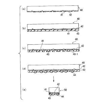
In Figure 8(a), a semiconductor wafer. 40 is
provided. The semiconductor wafer 40 is formed with a
number of IC's (integrated circuits) and includes a
plurality of electrode pads 41 on one surface of each of
the IC's for connection to the exterior. The IC's are in
the end form before being diced out from the semiconductor
wafer 40 as semiconductor chips. A region on the foregoing
one surface of each IC other than at the electrode pads 41
is covered with a passivation film 4,2 as in the prior art.
CA 02159243 1998-11-30
17
In Fig. 8(b), an adhesive layer 43 is formed over all the
area of one surface of the semiconductor wafer 40 where the
electrode pads 41 are formed. As a material of the
adhesive layer 43, photosensitive resin, such as
polyimide or epoxy, is used. The adhesive layer 43 is
about several micrometers to ten and several micrometers
in thickness and formed by the spin coating method. The
adhering a film of adhesive on the foregoing surface of the
sticking a film of adhesive on the foregoing side of the
semiconductor wafer 40.
In Fig. 8(c), for exposing each electrode pad 41
to the outside, an opening 43-1 is formed through the
adhesive layer 43 at a position corresponding to the
electrode pad 41. The openings 43-1 are formed by
chemical etching, but may also be formed by laser
processing. As shown in Fig. 10(a), the opening 43-1 is
provided for each electrode pad 41. Alternatively, as
shown in Fig. 10(b), each opening 43-1 may be formed into
an elongate shape for accommodating a plurality of
electrode pads 41. In the former case (Fig. 10(a)), the
openings 43-1 are arranged at regular pitches of about
50~ m, each having a width of about several tens of
micrometers to 100u m. In the latter case (Fig. 10(b)),
each opening 43-1 has a width of about 150u m.
In Fig. 8(d), electrodes 44 are formed at the
openings 43-1, respectively. Each electrode 44 is in the
form of a metal projection or a metal ball bump. In case
of the metal projection, the electrode 44 is formed by
CA 02159243 1998-11-30
18
plating. In this case, it is known to form an electrode
by coating a projection of copper (Cu) with gold (Au).
On the other hand, in case of the ball bump, while the
same materials may be used, it is preferable to use a
material which is a mixture of gold (Au) with palladium
(Pd) added thereto. The mixture of gold and palladium is
suitable for reducing the diameter of the ball bump, and
further achieves an effect of enhancing a joint strength
relative to later-described wiring layers on a carrier
film as compared with the foregoing materials forming the
metal projection.
As described later, the process of Fig. 8(d),
that is, the process of providing the electrodes 44, may
be omitted depending on the structure of the carrier film.
In Fig. 8(e), the IC's are diced out one by one
from the semiconductor wafer 40 as a semiconductor chip
50. When the electrodes 44 are formed by the ball bumps,
the processes in Figs. 8(d) and 8(e) may be reversed in
order.
In Fig. 9(a), a carrier film 60 is provided. The
carrier film 60 includes an organic insulating film 61
and wiring layers 62 formed on one of the main surfaces
of the organic insulating film 61 confronting the
semiconductor chip 50. A carrier film having wiring
layers on a surface remote from the semiconductor chip 50
will be described later. The organic insulating film 61
is formed with through holes 63 at portions corresponding
to the electrode pads 41, that is, the electrodes 44, and
CA 02159243 1998-11-30
19
further formed with through holes 64 at portions for
connection to an external board (not shown). These
through holes 63 and 64 are formed by the Ar laser
processing and the washing processing. The ultrasonic
processing may be the most suitable for the washing
processing. A metal material 65 is used to fill each
through hole 63 by plating, and a metal material 66 is
used to fill each through hole 64 by plating. The metal
material 65 used to fill the through hole 63 is used as a
medium for receiving a bonding tool 70 upon connection
between the electrode 44 and the wiring layer 62. The
metal material 65 may be omitted. The metal material 66
used to fill the through hole 64 works as an electrode for
connection to the external board, and thus is formed so as
to project slightly from the through hole 64. The material
forming the electrode 44 is used for the metal materials 65
and 66.
In the process in Fig. 9(a), the connection
between the wiring layers 62 of the carrier film 60 and
the electrodes 44 of the semiconductor chip 50 is
made. As is known, this connection is achieved by
applying the bonding tool 70 to the metal material 65 so
as to firmly attach the wiring layer 62 to the
corresponding electrode 44 under pressure.
In the process in Fig. 9(b), the carrier film 60
is pressed upon the semiconductor chip 50 while heating
the adhesive layer 43 so that the semiconductor chip 50
and the carrier film 60 are bonded together via the
CA 02159243 1998-11-30
adhesive layer 43.
In the process in Fig. 9(c), the carrier film 60
is cut approximately along the edge of the semiconductor
chip 50 so as to provide the semiconductor device the size
of a chip. Thereafter, as shown in Fig. 9(d), a ball
bump electrode 67 is formed at the tip of each metal
material 66 to work as an electrode for connection to the
external board. As a material of the ball bump electrode
67, solder is mainly used. In addition, Au or Au added
with Pd may also be used therefor.
Subsequently, in the process in Fig. 9(e), the
outer surfaces of the chip-size semiconductor device are
coated with a coating film 46 formed of a fluororesin
coating material using the spin coating method. The
coating film 46 is provided for preventing the insulation
failure due to an influx of water into the
semiconductor device via the joint portion between the
semiconductor chip 50 and the carrier film 60 and for
preventing an influx of water into the semiconductor
device through the organic insulating film 61. As
shown in Fig. 9(e), the spin coating is performed
onto the semiconductor device with the ball bump
electrodes 67 being located at the top. Accordingly, the
coating film 46 is formed substantially all over the
outer surfaces of the semiconductor device except at the
upper surface of the semiconductor chip 50. On the other
hand, since the region around the joint portion between
the semiconductor chip 50 and the carrier film 60 most
CA 02159243 1998-11-30
21
requires the reliable sealing, it may be possible to form
the coating film only at the region around the point
portion at a lateral side of the semiconductor device.
In the spin coating method, the coating film also
covers the ball bump electrodes 67. Thus, connection
failure is expected when connecting the ball bump
electrodes 67 to the external board. However, in
practice, since the fluororesin is poor in wettability
relative to metal, the thickness of the coating film formed
on each ball bump electrode 67 is small. Further, since
heat and pressure are applied to each ball bump electrode
67 upon connection to the external board, the coating
film on the ball bump electrode 67 tends to be broken and
thus raises no problem from a practical point of view.
In addition, each ball bump electrode 67 has a spherical
shape so that it is difficult for the fluororesin to
adhere to the ball bump electrode 67. This becomes more
significant by increasing the height of the ball bump
electrode 67. The coating film 46 may be formed by dipping
the semiconductor device into the fluororesin coating
material, instead of using the foregoing spin coating
method.
According to the foregoing first preferred
embodiment, the following effects can be achieved:
By forming the adhesive layer 43 on the
semiconductor wafer 40 before cutting the semiconductor
chips therefrom, the accurate positioning of the adhesive
film relative to the semiconductor chip is not required
CA 02159243 1998-11-30
22
as opposed to the prior art. Further, the adhesive layer
43 can be provided in a uniform thickness all over the
joint surface between the semiconductor chip 50 and the
carrier film 60. As a result, inclination of the
semiconductor chip 50 on the carrier film 60 can be
prevented, and the sealing at the joint portion between
the semiconductor chip 50 and the carrier film 60 can be
reliably achieved. Further, the region around the joint
portion between the semiconductor chip 50 and the carrier
film 60 at the lateral side of the semiconductor device
is coated with the coating film 46 so that the sealing is
further reliably ensured.
Further, in the process in Fig. 8(d), each
electrode 44 is formed so as to slightly project from the
corresponding opening 43-1 of the adhesive layer 43. As
a result, a gap is not formed relative to the
corresponding wiring layer 62, which would be otherwise
formed due to a step corresponding to the thickness of the
adhesive layer 43 as in the prior art. This means that
the connection between the electrode 44 and the wiring
layer 62 is achieved without deformation of the organic
insulating film 61. Thus, the connection between the
electrode 44 and the wiring layer 62 is not spoiled, and
the wiring layer 62 is not separated from the organic
insulating film 61, which would otherwise be caused due
to deformation of the organic insulating film 61.
Further, in the process in Fig. 9(a), since the
connection between the electrodes 44 and the wiring
CA 02159243 1998-11-30
23
layers 62 is performed before applying heat and pressure
to the adhesive layer 43, the openings 43-1 are prevented
from being closed due to the application of heat and
pressure to the adhesive layer 43 so that the connection
between the electrodes 44 and the wiring layers 62 is
reliably achieved.
Moreover, the through holes 63 and 64 of the
carrier film 60 are formed by the Ar laser processing and
the washing processing. The Ar laser processing is lower
in running cost as compared with the excimer laser
processing and is capable of rendering a non-tapered
through hole, that is, rendering a circumferential
wall of each through hole vertical. Further, the
diameter of the through hole can be rendered
less than 50u m. Thus, further narrowing of the pitches
of the through holes 63 and 64 can be realized. As
appreciated, in the inner-lead connection, narrowing of
the pitches of the through holes 63 is important. The
openings 43-1 of the adhesive layer 43 may also be formed
by the Ar laser processing.
Figs. 11(a) to 11(e) show a modification of the
first preferred embodiment. In the modification, the
carrier film differs from that of the first preferred
embodiment. Specifically, as shown in Fig. 11(a),
although the semiconductor chip 50 is the same as that in
the first preferred embodiment, a carrier film 60'
includes wiring layers 62' formed on the main surface of the
organic insulating film 61 opposite to the main surface
CA 02159243 1998-11-30
24
thereof confronting the semiconductor chip 50. In this
case, the organic insulating film 61 is formed with the
through holes, that is, the through holes 63, only at
portions corresponding to the electrodes 44. The through
holes 63 are formed by the Ar laser processing and the
washing processing as in the first preferred embodiment.
A metal material 65', which is the same as the metal
material 65, is used to fill the through holes 63 by
plating as in Fig. 9(a). The metal material 65' is used to
fill each through hole 63 so as to slightly project from
the main surface of the organic insulating film 61. The
wiring layers 62' are coated with a cover coating 68
formed of an insulating material. The cover coating 68
is formed with openings 68-1 at portions corresponding to
the metal material 65' and at portions for connection to
the external board.
In the process in Fig. 11(b), the connection
between the metal material 65' of the carrier film 60'
and each of the electrodes 44 of the semiconductor chip
50 is performed. This connection is achieved by applying
the bonding tool 70 to the wiring layer 62' via the
opening 68-1 corresponding to the metal material 65' so
as to firmly attach the metal material 65' to the
corresponding electrode 44 under pressure.
In the process in Fig. 11(c), the carrier film
60' is pressed upon the semiconductor chip 50 while
heating the adhesive layer 43 so that the semiconductor
chip 50 and the carrier film 60' are bonded together via
CA 02159243 1998-11-30
the adhesive layer 43.
In the process in Fig. 11(d), the carrier film
60' is cut approximately along the edge of the
semiconductor chip 50 so as to provide the semiconductor
device the size of a chip. Thereafter, as shown in Fig.
11(e), the ball bump electrode 67 is formed at the
opening 68-1 to work as an electrode for connection to
the external board. As a material of the ball bump
electrode 67, solder is mainly used. On the other hand,
Au or Au added with Pd may also be used therefor.
Subsequently, as described with reference to Fig.
9(e), the outer surfaces of the chip-size semiconductor
device are coated with the coating film formed of a
fluororesin coating material using the spin coating
method.
Now, a method of forming the bump electrode 67 as
described with reference to Fig. 11(e) will be described
with reference to Figs. 12(a) to 12(c). In Fig. 12(a),
an electrode pad 69 is formed by Au plating on the wiring
layer 62' exposed at the opening 68-1 for connection to
the external board. On this electrode pad 69 is formed
the bump electrode 67. For forming the bump electrode
67, a commercial solder ribbon 71 in the form of a plate
and a commercial special punching jig 72 are used. The
special punching jig 72 has the same function as a normal
punch, but differs from the normal punch in that a small
projection 72-1 is formed at its tip. A portion of the
solder ribbon 71 is punched out using the special
CA 02159243 1998-11-30
26
punching jig 72 so that a solder piece 71-1 punched out
from the solder ribbon 71 projects downward at its center
so as to have an essentially T-shape in section. As
shown in Fig. 12(b), a pressing force is applied to the
T-shaped solder piece 71-1 so as to temporarily join the
center of the solder piece 71-1 to the electrode pad 69.
Thereafter, the solder piece 71-1 is applied with flux
and heated so that, as shown in Fig. 12(c), the solder
piece 71-1 is formed into a ball shape so as to be the
bump electrode 67.
According to the foregoing method, the following
effects can be achieved in addition to the effects
achieved in the first preferred embodiment:
Specifically, since a sufficient amount of solder
is ensured for forming the bump electrode 67 and a
portion of the solder piece 71-1 is temporarily joined
to the electrode pad 69, even when a diameter of the
opening 68-1 is small, the connection between the bump
electrode 67 and the electrode pad 69 can be reliably
achieved. As appreciated, the processes shown in Figs.
11(a) to 11(e) and 12(a) to 12(C) are executed following
the process in Fig. 8(e).
Figs. 13(a) and 13(b) show another modification
of the first preferred embodiment. As in the
modification of Figs. 11(a) to 11(e), the carrier film
60' is formed with the wiring layers 62' on the surface
of the organic insulating film 61 opposite to the surface
thereof confronting the semiconductor chip 50. This
CA 02159243 1998-11-30
27
modification is applied to the case wherein the
electrodes 44 are not formed at the openings 43-1 of the
adhesive layer 43 in the process in Fig. 8(d) in the
first preferred embodiment. As in Figs. 11(a) to 11(e),
the metal material 65' is used to fill each of the
through holes 63 of the carrier film 60'. In this
modification, as shown in Fig. 13(a), a bump electrode
65-1' is further formed at the tip of the metal material
65'. As appreciated, a height of the bump electrode
65-1' is set no less than the thickness of the adhesive
layer 43.
In Fig. 13(b), after the connection between the
electrode pad 41 and the bump electrode 65-1' is
made using the bonding tool 70 in the same manner as
in Fig. 11(b), the bonding process is performed in the
same manner as in Fig. 11(c). The processes in Figs.
13(a) and 13(b) are performed between the process in Fig.
8(e) and the process in Fig. 11(c). Accordingly, this
modification achieves effects which are substantially the
same as those achieved in the modification of Figs. ll(a)
to 11(e) and 12(a) to 12(c).
Fig. 14 shows a relationship between the diameter
of a material (Au added with Pd) when pressed to another
member and the shear strength thereof, wherein the material
is used for, for example, the bump electrode or the ball
bump electrode. As appreciated from Fig. 14, the
strength becomes greater as the amount of Pd added
increases and as the heating temperature increases.
CA 02159243 1998-11-30
28
Now, a second preferred embodiment of the present
invention will be described with reference to Figs. 15(a)
to 15(h). In the second preferred embodiment, the
adhesive layer 43 described in the first preferred
embodiment is formed on the carrier film, and the diced-
out semiconductor chip is used: Further, in the second
preferred embodiment, the carrier film includes the
wiring layers on the surface of the organic insulating
film confronting the semiconductor chip, as described
with reference to Fig. 9(a).
In Fig. 15(a), a two-layer base member in the
form of the organic insulating film 61 (for example,
25u m in thickness) and a copper foil 62a (for example,
18u m in thickness) stacked on one of the main surfaces
of the organic insulating film 61 is provided. In
Fig. 15(b), the pattern etching is performed on the
copper foil 62a so as to form the wiring layers 62. In
Fig. 15(c), the adhesive layer 43 is formed on a surface of
the organic insulating film 61 where the wiring layers 62
are formed. The adhesive layer 43 is formed by the spin
coating method or by sticking the adhesive film as in the
foregoing first preferred embodiment.
In Fig. 15(d), the organic insulating film 61 is
formed with the through holes 63 and 64, and the adhesive
layer 43 is formed with the openings 43-1. As described
in the first preferred embodiment, it is preferable that
the through holes 63 and 64 are formed by the Ar laser
processing and the washing processing. On the other
CA 02159243 1998-11-30
29
hand, the chemical etching may be used for forming the
through holes 63 and 64. The openings 43-1 may also be
formed by the Ar laser processing or the chemical
etching.
In Fig. 15(e), the metal material 65 is used to
fill the through holes 63 by plating, and the metal
material 66 is used to fill the through holes 64 by
plating. A metal material 75 is also used to fill the
openings 43-1 by plating. As described with reference to
Fig. 9(a), the use of the metal material 65 to fill the
through holes 63 may be omitted. Further, the use of the
metal material by plating may be performed only for
the through holes of the organic insulating film 61. In
this case, the openings 43-1 of the adhesive layer 43 are
provided with ball-shaped bump electrodes each formed of
Au or Au added with Pd. As appreciated, these bump
electrodes may be provided at the semiconductor chip 50
rather than at the openings 43-1.
In Fig. 15(f), the diced-out semiconductor chip
50 is provided: In the process in Fig. 15(g), the metal
material 75 is connected to each of the electrode pads
41. As described with reference to Fig. 9(a), this
connection is achieved by applying the bonding tool 70 to
the metal material 65 so as to firmly attach the metal
material 75 to the corresponding electrode pad 41 unde r
pressure. Thereafter, as described with reference to
Fig. 9(b), by applying heat and pressure, the
semiconductor chip 50 and the carrier film 60 are bonded
CA 02159243 1998-11-30
together via the adhesive layer 43 interposed
therebetween.
Subsequently, in Fig. 15(h), as described with
reference to Fig. 9(d), the bump electrode 67 is provided
at the tip of the metal material 66, and the carrier film
60 is cut into a chip size so that the semiconductor
device is obtained. Thereafter, as described with
reference to Fig. 9(e), the outer surfaces of the
semiconductor device, particularly the lateral side
thereof, are coated with the coating film formed of the
fluororesin coating material.
Figs. 16(a) to 16(g) show a modification of the
second preferred embodiment. In this modification, the
organic insulating film 61 is used so as to locate the
wiring layers formed thereon at the surface remote from the
semiconductor chip. Accordingly, in Fig. 16(a), the
adhesive layer 43 is formed on the main surface opposite
to the main surface where the wiring layers 62' are
formed. The adhesive layer 43 is formed in the same
manner as in the first preferred embodiment. When adhesion
between the adhesive layer 43 and the organic insulating
film 61 is insufficient, the plasma ashing or the UV
(ultraviolet) irradiation may be applied to the surface
of the organic insulating film 61 where the adhesive layer
43 is to be formed, so as to improve the adhesion
therebetween.
In Fig. 16(b), for connection between each wiring
layer 62' and the corresponding electrode pad of the
CA 02159243 1998-11-30
31
semiconductor chip, the opening 43-1 and the through hole
63 are formed by the Ar laser processing so as to
penetrate the adhesive layer 43 and the organic
insulating film 61, respectively. In Fig. 16(c), the
through hole 63 and the opening 43-1 are filled with a
metal material 76 by plating. The tip of the metal
material 76 is arranged to project sufficiently from the
adhesive layer 43. On the other hand, in Fig. 16(d), the
main surface of the organic insulating film 61 at a side
of the wiring layers 62' is coated with the cover coating
68. The openings 68-1 are formed by the Ar laser
processing at portions corresponding to the metal
material 76 and at portions for connection to the
external board.
Thereafter, in Fig. 16(e), the semiconductor chip
50 is provided. In Fig. 16(f), the connection between
the metal material 76 and each of the electrode pads 41
of the semiconductor chip 50 is achieved in the same
manner as in Fig. 13(b). Subsequently, the semiconductor
chip 50 and the carrier film 60' are bonded together via
the adhesive layer 43 interposed therebetween. Further,
the carrier film 60' is cut into a chip size, and as
shown in Fig. 16(g), the ball bump electrodes 67 are
provided at the openings 68-1 of the cover coating 68 for
connection to the external board. As appreciated,
thereafter, the outer surfaces of the semiconductor
device, particularly the lateral side thereof, are coated
with the coating film formed of the fluororesin coating
CA 02159243 1998-11-30
32
material. The processes in Figs. 16(a) to 16(g) are
executed following the process in Fig. 15(b).
In the second preferred embodiment, the adhesive
layer 43 is formed on the carrier film and bonded to the
cut-out semiconductor chip 50. Alternatively, the
adhesive layer may be formed on a surface of the diced-
out semiconductor chip 50 where the electrode pads 41 are
formed, so as to cover all the area thereof.
Specifically, after forming the adhesive layer on the
diced-out semiconductor chip 50, the openings are formed
by the laser processing or the chemical etching at
portions of the adhesive layer corresponding to the
electrode pads 41. Thereafter, by using the metal
material to fill these openings by plating or by providing
the ball bump electrodes at the openings, the
semiconductor chip 50 having the adhesive layer 43 as
shown in Fig. 8(e) can be produced.
Either of the second preferred embodiment and the
modification thereof can achieve effects similar to those
achieved in the first preferred embodiment.
Figs. 17(a) and 17(b) show another modification
of the second preferred embodiment. In this modifica-
tion, as in the second preferred embodiment, the carrier
film 60 is formed with the wiring layers 62 at the surface
confronting the semiconductor chip 50. On the other
hand, as shown in Fig. 17(a), the filling of the openings
43-1 of the adhesive layer 43 by plating with the metal
material is not performed as opposed to the process in
CA 02159243 1998-11-30
33
Fig. 15(e). Thus, the semiconductor chip 50 is provided
with the bump electrodes 47 on the electrode pads 41.
In Fig. 17(b), after the connection between the
wiring layers 62 and the bump electrodes 47 is achieved
using the bonding tool 70 in the same manner as in Fig.
15(g), the semiconductor chip 50 and the carrier film 60
are bonded together via the adhesive layer 43 interposed
therebetween. The processes in Figs. 17(a) and 17(b) are
executed instead of the processes in Figs. 15(e) to
15(g). Accordingly, this modification achieves effects
similar to those achieved in the second preferred
embodiment.
Fig. 18 is a diagram for explaining an example,
wherein the directional matching is easily achieved upon
mounting the semiconductor device onto the external
board. In this example, a mark for achieving the
directional matching is formed by using a portion of the
wiring layers 62 of the carrier film. In general, the
wiring layers of the carrier film are formed by etching
the copper foil of the two-layer base member (see Fig.
15(a)) so that the etching regions are as small
as possible. This is appreciated from Fig. 18, wherein
the etching regions are represented by solid lines which
are very small. As a result, the wiring layers tend to
remain largely at the center of the carrier film. In
Fig. 18, an opening 62-2 is formed in the copper foil which
remains as a wiring layer 62-1 at the center of the
carrier film during the etching process. A user
CA 02159243 1998-11-30
34
memorizes the opening 62-2 and configuration of the
wiring layers around the opening 62-2 in advance. As a
result, when mounting the semiconductor device onto the
external board, the user can easily fudge which surface of
the rectangular semiconductor device should be the upper
surface. For example, in Fig. 18, the directional matching
is achieved by setting an edge 62-3 of the wiring layer
62-1 formed with the opening 62-2 to be an upper side.
If a shape of the opening 62-2 is not circular,
but is capable of identifying a particular direction,
such as an isosceles triangle, the directional matching
can be achieved more easily. Further, if no wiring
layers remain at the center of the carrier film, the
opening may be formed at the organic insulating film 61.
In any case, the foregoing directional matching mark in
the form of the opening may apply to any of the foregoing
preferred embodiments, w
While the present invention has been described in
terms of the preferred embodiments, the present invention
can be embodied in various other ways. For example, the
processing of the through holes 63 and 64 is not limited
to the Ar laser processing, but may be the excimer laser
processing or the carbon dioxide laser processing. On
the other hand, the openings 43-1 of the adhesive layer
43 may be formed by the Ar laser processing. Further, in
any of the foregoing preferred embodiments, the formation
of the fluororesin coating film on the outer surfaces of
the semiconductor device may be omitted.
CA 02159243 1998-11-30
As described above, the following effects can be
achieved according to the foregoing preferred
embodiments:
A. The semiconductor chip and the carrier film
are bonded together via the adhesive layer extending all
over the joint surface therebetween. Accordingly, the
adhesive layer can be interposed uniformly between the
semiconductor chip and the carrier film, and thus the
sealing around the joint portion therebetween can be
reliably achieved. Since the openings required at the
adhesive layer for the electrical connection can be
formed by the fine processing, such as the laser
processing or the chemical etching, these openings can be
formed with high positional accuracy.
B. At least the lateral side of the
semiconductor device, that is, the region around the
joint portion between the semiconductor chip and the
carrier film, is coated with the coating film.
Accordingly, deterioration of the joint portion due to
the heating process and the washing process required for
mounting onto the external board can be prevented so that
protection from moisture is further improved.
C. The steps or gaps caused by forming the
openings at the adhesive layer are eliminated by using
the metal material to fill the openings or by providing the
ball bump electrodes at the openings. By using Au added
with Pd as a material of the ball bump electrode, the
joint strength can be enhanced so that a diameter of the
CA 02159243 1998-11-30
36
ball bump electrode can be reduced to achieve narrowing
of the pitches of the ball bump electrodes.
D. In the case where carrier film has the wiring
layers on the surface thereof opposite to its surface
confronting the semiconductor chip, each of the ball bump
electrodes is provided by soldering at the corresponding
opening of the cover coating provided for coating the
wiring layers. Accordingly, a controlled amount of the
solder can be used. Particularly, by using the special
punching jig for forming the ball bump electrode, the
ball bump electrode can be formed from the solder piece.
E. In the case where the through holes at the
organic insulating film or the openings at the adhesive
layer by the Ar laser processing, the finer processing
can be achieved. Thus, the diameter of the through hole
can be reduced, and further, the circumferential wall of
the through hole can be vertical. As a result, narrowing
of the pitches of the through holes can be achieved.