Note: Descriptions are shown in the official language in which they were submitted.
CA 02159253 2005-02-10
LINEAR ELECTRON BEAM TUBE
This invention relates to electron beam tubes and more particularly to input
resonator
cavities of such tubes at which high frequency energy is applied.
The present invention is particularly applicable to inductive output tetrode
devices
(hereinafter referred to as "IOT's") such as those referred to by the trade
name Klystrode
(Registered Trade Mark, Varian Associates Inc.)
An IOT device includes an electron gun arranged to produce a linear electron
beam
and an input resonant cavity at which an r.~ signal to be amplified is applied
to produce
modulation of the beam at a grid of the electron gun. The resultant
interaction between the
r.f. energy and the electron beam causes amplification of the high frequency
signal which is
then extracted from an output resonant cavity.
During operation of the tube, electrodes of the electron gun must be operated
at
relatively high voltages, of the order of tens of kilovolts, and this may
cause problems,
especially as the input cavity may form an external part of the IOT and
therefore be handled
during normal usage of the device. The present invention arose from an attempt
to provide
an improved IOT input cavity arrangement but is also applicable to other types
of linear
electron beam devices having input resonant cavities.
2 P/60454/V POW
According to the invention, there is provided a linear electron beam tube
comprising:
an input cavity which is substantially cylindrical about a longitudinal axis
and
arranged to receive, in use, a high frequency signal to be amplified;
an electron gun arranged to produce an electron beam in a substantially
longitudinal
direction; and
an output cavity from which the amplified high frequency signal is extracted;
wherein
the input cavity substantially surrounds the electron gun and comprises an
inner body
portion electrically connected to part of the electron gun and an outer body
portion
electrically insulated from the inner body portion, the inner body portion
being maintained at
a relatively high voltage compared to that of the outer body portion, and
wherein the inner and outer body portions each include an axially extensive
metallic
portion substantially coextensive in an axial direction with ceramic material
being located
between the metallic portions.
By "high voltage" it is meant of the order of tens of kilovolts.
The use of the invention enables parts of a linear electron beam tube which
operate at
relatively high voltages to be located such that they are not readily
accessible during normal
operation of the tube. In addition, the arrangement of the metallic portions
of the inner and
outer body portions and the ceramic material located between them acts as an
rf choke. This
enables the two body portions to be separated to achieve the desired
electrical isolation
between them whilst permitting the input cavity to be such that there is low
rf leakage from
it, thereby affording efficient operation.
3 P/60454/V POW
The use of ceramic material as part of the r.f. choke in accordance with the
invention
offers a number of important advantages. The ceramic material maintains its
shape even at
very high temperatures, of the order of 100(~C or more, and remains rigid at
these high
temperatures. The ceramic material may be readily machined or otherwise
fabricated into the
desired shape, which in one particularly advantageous embodiment is
substantially
cylindrical being located coaxially with the longitudinal axis of the tube.
The ceramic
provides good voltage hold-off over the range of temperatures encountered
during operation.
The ceramic material also provides a surface onto which the metallic portions
can be fixed.
These portions may advantageously comprise metallised regions of the ceramic
surface but
in some embodiments they may be formed as separate components fixed to the
ceramic
surface. The ability to metallise the ceramic surface allows high accuracies
to be achieved in
positioning the metallic portions relative to one another. Also, if for any
reason it is
necessary to remove or replace the ceramic tube during servicing,
metallisation of its
surfaces enables this to be relatively easily carried out.
The structural integrity offered by the use of the ceramic material allows the
tube to
undergo thermal cycling without significant distortion of the choke, offering
good lifetimes
for the tube as a whole.
As the ceramic material maintains its configuration during operation of the
tube, even
at higher temperatures, it does not require the metallic portions to offer
support to hold it in
shape. Again, this allows a metallisation layer to be used rather than a
separate metal
component to define the choke, with the consequent advantages in accuracy of
the choke
dimensions and fabrication as mentioned previously. In a particularly
advantageous
4 P/60454/V POW
embodiment of the invention, the ceramic material is extensive in the axial
direction beyond
the choke. This may be used for example as a shield against arcing in the tube
between parts
which are at different electrical potentials.
In one advantageous embodiment of the invention, electrically insulating
material of
a different type covers at least some of the ceramic material. This may be,
for example,
silicone rubber. This may also be included over at least some of the metallic
portions to
provide additional shielding. It is supported in position by the ceramic
material.
The metallic portions of the r.f. choke extend in substantially the same
direction and
hence are substantially parallel to each other. This is particularly
advantageous as it reduces
electrical stresses and therefore the tendency of voltage breakdown to occur
between the
inner and outer body portions, even at high voltages.
It is preferred that the metallic portions are substantially cylindrical, as
this is a
symmetrical configuration which is usually desirable in linear electron beam
tubes as it gives
good electrical characteristics and results in a mechanically robust
arrangement.
Preferably, each of the inner and outer body portions includes two metallic
portions
extensive in an axial direction outwardly from the input cavity, there thus
being two pairs of
co-extensive metallic portions. Such an arrangement minimizes r.~ losses in
the region
between the inner and outer body portions. Although the input cavity could
alternatively
comprise only one such pair, this would tend to result in an r.~ leakage path
being present
between other parts of the cavity.
P/60454/VPOW
It is preferred that the inner body portion comprises two sections which are
electrically separate from one another. Again, this facilitates manufacture
and assembly and
advantageously also permits different voltages to be applied to different
parts of the electron
gun via the inner body portion. In one preferred embodiment of the invention,
the inner
body portion is electrically connected to a cathode and a grid of the electron
gun. Where two
sections are included, one of them may be physically and electrically
connected to the
cathode and the other to the grid.
Where two pairs of rf chokes are included in the arrangement, the ceramic
material
may be present as two separate rings, for example, one ring being interposed
between one
pair of metallic portions and the other between the other pair. Alternatively,
and preferably,
the electrically insulating material is a unitary member which is extensive
between both pairs
of metallic portions Advantageously, the inner and outer body portions are
physically joined
together by the ceramic material.
Preferably, the outer body portion is at ground potential.
Some ways in which the invention may be performed are now described by way of
example with the reference to the accompanying drawings in which:
Figure 1 is a schematic sectional view of an IOT in accordance with the
present
invention, some parts of which have been omitted for sake of clarity; and
Figure 2 schematically illustrates part of another IOT in accordance with the
1 2159253
6 P/60454/V POW
invention.
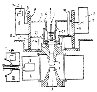
With reference to Figure l, an IOT comprises an electron gun 1 which includes
a
cathode 2 and grid 3 arranged to produce an electron beam along the
longitudinal axis X-X
of the arrangement. The IOT includes drift tubes 4 and 5 via which the
electron beam passes
before being collected by a collector (not shown). A cylindrical input
resonant cavity 6 is
arranged coaxially about the electron gun 1 and includes an input coupling 7
at which an r.f.
signal to be amplified is applied. An output cavity 8 surrounds the drift
tubes 4 and 5 and
includes a coupling loop 9 via which an amplified r.~ signal is extracted and
coupled into a
secondary output cavity 10 and an output coupling 11.
During operation of this device, the cathode 2 and grid 3 are maintained at
potentials
of the order of 30kV, the grid 3 being maintained at a do bias voltage at
about 100 volts less
than the cathode potential. The input high frequency signal applied at 7
results in an r.f.
voltage of a few hundred volts being produced between the cathode 2 and the
grid 3.
The input cavity 6 is defined by an inner body portion 12 and an outer body
portion
13 with ceramic material in the form of a cylinder 14 between them, the inner
body portion
12 being electrically insulated from the outer body portion 13 by the
intervening ceramic
material 14. The outer body portion 13 is maintained at substantially ground
potential, thus
facilitating safe handling of device, whilst the inner body portion 12 is
maintained at much
higher voltages.
The outer body portion includes two annular plates 15 and 16 arranged parallel
to one
7 P/604541VPOW
another and transverse to the longitudinal axis X-X with a cylindrical outer
section 17. The
inner body portion 12 comprises two sections. The first section 20 is
mechanically and
electrically connected to the cathode 2 and the second section 21 is
mechanically and
electrically connected to the grid 3. In the embodiment shown, a ceramic
cylinder 22 is
located between the sections 20 and 21 to give additional mechanical support
to the
assembly.
The ceramic cylinder 14 provides electrical insulation between the inner body
portion
12 and the outer body portion 13 and also forms part of rf choke means to
substantially
prevent leakage of high frequency energy from the cavity 6. The plate 15 of
the outer body
portion 13 is arranged adjacent a metallised layer 18 on the outer surface of
the ceramic
cylinder 14 extending around it in the circumferential direction. The section
20 of the inner
body portion 12 is arranged adjacent the inner surface of the cylinder 14 and
also is in
contact with metallisation 19 extending circumferentially within the cylinder
14. The
metallisation layers 18 and 19 and the intervening part of the ceramic
cylinder 14 together
define an rf choke. Similarly, the annular plate 16 of the outer body portion
13 is in contact
with metallisation 23 and the section 21 with meta.llisation 24 to define a
second rf choke.
The metallisation layer on the outer surface of the ceramic may be longer or
shorter in the
longitudinal axial direction than the corresponding metallisation layer on the
inner surface of
the cylinder 14.
In other embodiments of the invention, one or more of the metallisation layers
may be
replaced by a separately formed metal cylinder which is located adjacent the
ceramic
cylinder 14.
~~.~~?~3~
8 P160454/VPOW
A power lead 26 is routed via an aperture in the section 20 to supply the grid
3 with
the appropriate bias voltage, the connection being made via the lead 26 to the
section 21.
Part of another IOT similar to that of Figure 1 is shown in Figure 2. In this
embodiment, a single ceramic cylinder 27 similar to that of the Figure 1
embodiment is used
and again, metallisation is laid down on the surfaces to define two rf chokes.
At one end of
the ceramic cylinder 27, a layer of silicone rubber 28 is arranged to cover
the end of the
cylinder and its inner and outer surfaces and part of the metallisation
layers. The inner
surface of the silicone rubber 28 includes a plurality of circumferential
grooves 29 to
improve voltage hold-off ability.