Note: Descriptions are shown in the official language in which they were submitted.
. 2159273
PROTECTION OF ACTIVE TELEPHONE LINE INTERFACE CIRCUITS
This invention relates to telephone line interface circuits, and is particularlyconcerned with a telephone line int~rf~ce circuit which includes an active line drive circuit,
and with the protection of the line drive circuit from transient voltages which can occur in
S normal use of the line inttorf~ce circuit.
Background of the Invention
Active telephone line interface circuits, in which the tip and ring wires of a
telephone subscriber line are driven via an active line drive circuit, are known. This
invention is particularly applicable to, but is not in any way limited to, a form of active
10 telephone line interface circuit certain features of which are described in Rosch et al.
United States Patent No. 5,274,702 issued December 28, 1993 and entitled "Wideband
Telephone Line Interface Circuit" and Rosenbaum et al. United States Patent No.
5,3237461 issued June 21, 1994 and entitled "Telephone Line Tnterf~e Circuit With
Voltage Switching".
As described in these patents, in a telephone subscriber line interface circuit a line
drive circuit includes two unity-gain d.c. amplifiers whose outputs are coupled to the tip
and ring wires, respectively, of the telephone subscriber line via a ~,wi~ching circuit and a
sensing circuit. The line intPrf~ce circuit also includes a controlled voltage generator and a
control circuit. The sensing circuit serves to monitor a.c. and d.c. conditions on the line
20 and includes a sensing transformer and series resistors which are generally referred to as
feed resistors. The switching circuit serves, in association with software control via the
control circuit, to interconnect the line, line drive circuit, controlled voltage generator, and
a battery in various configurations to provide for dirr~ t operating states of the line
interface circuit. These states include configurations in which relay contacts connect the
25 outputs of the line drive circuit or the output of the controlled voltage generator selectively
to the tip and ring wires of the line, and in which relay contacts and an electronic switch
selectively connect the output of the controlled voltage generator or the battery as a supply
voltage for the line drive circuit.
It is desirable for the software control of the controlled voltage generator and the
30 switching circuit to be such that switching operations to close relay contacts only take
place at times when there are in~ignificant voltage dirrt;lc;llces across the relay contacts, so
that high current flow on switching, and consequent damage to the relay contacts, is
avoided. In practice, however, the desire for relatively rapid ~,wi~ching operations, and
especially the inductive and generally unknown nature of the telephone subscriber line to
35 which the line interface circuit is connected, result in conditions in which substantial
voltage differences can exist across the closing relay contacts. In consequence, there can
be a temporary high current flow which damages the relay contacts.
2159273
It is also well known to protect the line drive circuit in an active subscriber line
interface circuit from high transient voltages due to lightning, a.c. surges, and inductive
coupling. To this end, it is known to couple a diode bridge to points between the outputs
of the line drive circuit and the feed resistors, for clamping positive transient voltages to
5 ground and for clamping negative transient voltages to a breakdown voltage of a transient
voltage suppressor which is connected between a negative supply voltage and ground. In
order to provide sufficient power ~ sip;~tinn for negative transient voltages, it has been
necessary to use several transient voltage suppression diodes (frequently referred to by the
trade name TRANZORB or TRANSIL) in combination. This has the disadvantages of
10 incurring a relatively high cost and requiring a relatively large physical space.
It would be desirable to be able to replace the several transient voltage suppression
diodes by a single crowbar-type protection device, frequently referred to by the trade
name TRISIL or SIDAC. However, such a device has the disadvantage that, if used in an
active line interface circuit, the current supplied by the line drive circuit can be sufficient to
15 maintain the protection device operative at and after the end of a negative transient voltage,
resulting in a locked up state of the line interface circuit.
For the avoidance of any doubt, it is observed here that the TRANZORB and
TRANSIL type of transient voltage suppression diodes are avalanche diodes which are
specially designed to clamp excessive voltages (i.e. they provide a voltage clamping
20 function) and to dissipate high transient power. In this specification they are referred to as
transient voltage suppressors, and they are illustrated in the drawings in the same manner
as zener diodes. In contrast, the TRISIL or SIDAC crowbar-type protection device has an
electrical characteristic similar to that of a triac but with an internal triggering mech~ni~m;
it provides a very high impedance or open circuit for voltages up to a breakover voltage,
25 and then provides a low impedance or short circuit as long as a holding current is
m~int:~ined. In this specification this device is referred to as a crowbar-type protection
device, and is illustrated in the drawings in the same manner as a triac but with a
breakover bar instead of a trigger input.
An object of this invention is to provide an improved telephone line interface
30 circuit in which the above disadvantages of the prior art are reduced or avoided.
Summary of the Invention
According to one aspect of this invention there is provided a telephone line
interface circuit comprising: two amplifiers having outputs coupled via tip and ring paths
to tip and ring terminals, respectively, for connection to a two-wire telephone line; a diode
35 bridge having two a.c. terminals coupled to the tip and ring paths, respectively, a positive
d.c. termin~l coupled to ground, and a negative d.c. termin~l; a crowbar-type protection
device coupled between the negative d.c. termin~l of the diode bridge and ground,
responsive to a negat*e transient voltage at the negative d.c. termin~l of the diode bridge
215927~
exceeding a threshold level to short the transient voltage to ground; a negative supply
voltage line for the amplifiers; a capacitor coupled between the negative supply voltage
line and ground; a diode coupled between the negative supply voltage line and the negative
d.c. terminal of the diode bridge with a polarity such that the diode is reverse biased when
the protection device shorts said negative transient voltage to ground; and circuitry
responsive to the short of the negative transient voltage to ground for reducing current
supplied by the amplifiers to below a holding current for m~int~ining the short by the
protection device.
In one embodiment of the invention, the two amplifiers comprise d.c. amplifiers
and the circuitry for reducing current supplied by the amplifiers comprises two diodes,
each connected between the negative d.c. terminal of the diode bridge and a non-inverting
input of a respective one of the amplifiers with a polarity to conduct when the protection
device shorts the negative transient voltage to ground.
In another embodiment of the invention, the cil.;uiLly for reducing current supplied
by the amplifiers comprises a circuit for reducing current supplied to the negative voltage
supply line so that the capacitor discharges. The telephone line interface circuit can further
include a switching circuit including relay contacts for switching a supply voltage to the
negative supply voltage line for charging the capacitor; and a current limiting circuit in
series with the relay contacts for limiting charging current to the capacitor when the relay
contacts close; in this case preferably the circuit for reducing current supplied by the
~mplifiers comprises a circuit for controlling the current limiting circuit.
In a pr~;r~lled form, the current limiting circuit comprises: a current sensor and a
controlled path of a transistor connected in series with the relay contacts for supplying
charging current to the capacitor; and a control circuit responsive to voltage dropped
across the current sensor for controlling the transistor to limit current through the
controlled path of the transistor; and the circuit for controlling the current limiting circuit is
responsive to reverse biasing of the diode to control the control circuit to substantially
elimin~te current through the controlled path of the transistor.
The current sensor preferably comprises a resistance and an inductance in series.
On closing of the relay contacts, the presence of the inductance not only reduces an initial
current for charging the capacitor, but also increases the voltage dropped by the current
sensor so that a turn-on delay of the current limiting circuit is reduced. Deterioration of
the relay contacts, which can otherwise occur due to the high charging current
imme~ tt-,ly on closing of the contacts, is thereby avoided.
Thus according to another aspect this invention provides an electronic circuit
comprising a capacitor for smoothing a supply voltage, relay contacts via which the
capacitor is charged to the supply voltage, and a current limiting circuit connected in series
with the relay contacts for limiting charging current to the capacitor on closing of the relay
215g273
contacts, the current limiting circuit comprising a current sensor and a controlled path of a
transistor connected in series with the relay contacts for supplying charging current to the
capacitor; and a control circuit responsive to voltage dropped across the current sensor for
controlling the transistor to limit current through the controlled path of the transistor,
wherein the current sensor comprises a resistance and an inductance in series.
Thus the invention provides the advantages that a c owbal--type protection device
can be used without resulting in a locked up state of the line interface circuit, and that this
can be achieved using a simple diode arrangement or using the current limiting circuit
which also prevents damage to the relay contacts. The inductor in the current limiting
circuit provides the advantages of improved current limiting and more rapid switching of
the current limiting circuit.
Brief Description of the Drawings
The invention will be further understood from the following description with
reference to the accompanying drawings, in which:
Fig. 1 is a schematic diagram illustrating relevant parts of a known form of
telephone line int~rf~ce circuit;
Fig. 2 is a similar schematic diagram illustrating the telephone line int-orf~re circuit
including a current limiting circuit in accordance with one embodiment of this invention;
and
Figs. 3 and 4 are similar schematic diagrams illustrating modified forms of the
telephone line interface circuit in accordance with other embodiments of this invention.
Detailed Description
Referring to Fig. 1, there is illustrated a schematic diagram showing parts of an
active telephone line interface circuit, which is assumed in the following description to
form part of and be located at a telephone central office (not shown), or CO, but which
may :~ltrrn:~tively form part of a remote trrrnin~l which is coupled to a CO via a
multiplexed commllnications path. Only those parts of the line interface circuit which are
relevant to a full understanding of this invention are shown in Fig. 1.
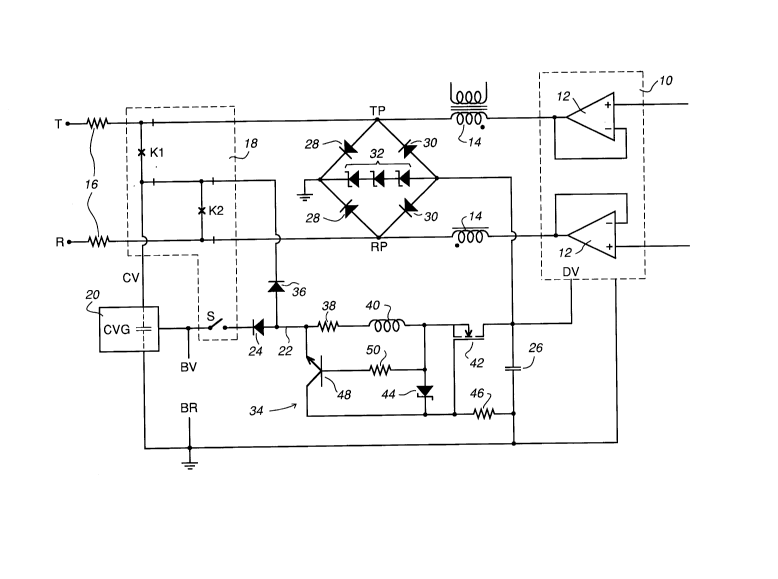
The line interface circuit comprises a line drive circuit 10 which comprises two unity-gain d.c. amplifiers 12 shown within a broken line box. The outputs of theamplifiers 12 constitute outputs of the line drive circuit 10 and are coupled to termin~ T
and R, for connection respectively to the tip and ring wires of a two-wire telephone
subscriber line (not shown), via transformer windings 14 and feed resistors 16 of a
sensing circuit which is not otherwise shown, and via a ~.wi~chillg circuit 18 which
includes an electronic switch S and relay contacts Kl and K2 of two latching relays. The
line interface circuit also includes a controlled voltage generator (CVG) 20 which is
supplied from a CO battery voltage BV (for example -48 volts) and battery return line BR,
at zero volts or ground potential, to produce a controlled voltage CV under the control of a
- 215927~
digital control circuit which is not shown. The control circuit also controls the operation
of the switching circuit 18 and d.c. voltages supplied to inputs of the line drive circuit 10,
coupled to non-inverting (+) inputs of the amplifiers 12, for det~",li~ g d.c. output
voltages of the amplifiers 12.
Further details of the line drive circuit 10, the sensing circuit, the switching circuit
18, the control circuit, and the operation of these are contained in United States Patents
Nos. 5,274,702 and 5,323,461 already referred to. The CVG 20 can be as further
described in Rosenbaum et al. United States Patent No. 5,103,387 issued April 7, 1992
and entided "High Voltage Converter". This generator includes an output capacitor which
is illustrated in Fig. 1 widhin the box representing the CVG 20, with connections shown
by broken lines between the output for the controlled voltage CV and ground.
The relay contacts Kl and K2 are shown in a reset state of the relays having oneopen contact (represented by an X) and two closed contacts (each represented by a vertical
bar), one of which is in the path from the output of a respective amplifier 12 to the
respective termin:~l T or R, and the other of which is in a series padh from dhe output of the
CVG 20 to a line 22 for supplying the line drive circuit 10 with a supply voltage DV. In
this state the switch S, which is connected in series with a diode 24 between the battery
voltage BV and the supply line 22, is open, and the CVG 20 is controlled to generate the
controlled voltage CV to constitute the line drive circuit supply voltage DV. The diode 24
serves to prevent contention between the voltages CV and BV.
In another operating state, the CVG 20 is controlled to be inactive, so that itsoutput presents a high impedance, and the switch S is closed so that dhe battery voltage
BV is connected to the line 22 to constitute the line drive circuit supply voltage DV. Other
operating states of the ,wi~hillg circuit 18 and the CVG 20 serve for example to supply
ringing or other high sign~lling voltages generated by the CVG 20 to the t~rmin~l T or R,
one of the relays being set accordingly to change the states of the contacts Kl or K2.
As also illustrated in Fig. 1, the supply voltage DV for the line drive circuit 10 is
smoodhed by a capacitor 26, having a capacitance for example of l ,uF and being
connected between the line 22 and ground. Ful~he~ ore, the line interface circuit includes
a diode bridge formed by two diodes 28 and two diodes 30, and dlree transient voltage
suppressors which are connected in series with one another and are collectively referenced
32. The diode bridge has a.c. terminals connected to points TP and RP, between the
switching circuit 18 and dle transformer windings 14 in the transmit and receive paths
from the outputs of dhe amplifiers 12 to the terminals T and R respectively. A positive
d.c. t.ormin~l of the diode bridge is connected to ground, and a negative d.c. t~rmin~l of
the diode bridge is connected to the line 22. The transient voltage suppressors 32 are
connected between the d.c. termin~l~ of the diode bridge.
215 9273
In normal operation, the line drive circuit 10 is controlled by the control circuit so
that the output of the amplifier 12 which is coupled to the tip wire t.ormin~l T has a slightly
negative voltage with respect to ground, for example -5 volts, and so that the output of the
amplifier 12 which is coupled to the ring wire terrnin~l R has a slightly positive voltage
S with respect to the supply voltage DV, for example -45 volts when the supply voltage DV
is -50 volts. In the event of a lightning strike on the telephone line or a fault condition
producing a positive transient voltage at one or both of the points TP and RP, current
(limited by the feed resistors 16) is conducted to ground via one or both of the diodes 28.
In the event of a lightning strike on the telephone line or a fault condition producing an
10 excessive negative transient voltage at one or both of the points TP and RP, current
(lirnited by the feed resistors 16) is conducted to the negative voltage supply line 22 via
one or both of the diodes 30. The maximum negative voltage of this line 22 is limited to
the breakdown voltage of the transient voltage suppressors 32; for example this can be
about -64 volts.
In the line interface circuit as described above, in order to provide the supplyvoltage DV for the line drive circuit 10 from the controlled voltage CV, which for example
may be up to -56 volts, the capacitor 26 is charged upon closing of the relay contacts Kl
and K2 in the path from CV to DV. In the absence of a current limiter in this path, the
initial charging current can be very high, for example about 20 Amps. This high current
being switched by the relay contacts Kl and K2 can cause deterioration of the relay
contacts and consequent unreliability due to sticking contacts. This problem can be
exacerbated by the inductive nature of the telephone subscriber line to which the output of
the CVG 20 may just previously have been connected via the relay contacts Kl and K2,
which in conjunction with the output capacitor of the CVG 20 may cause the controlled
voltage CV to be at a relatively uncontrolled level.
A potential solution to this problem is to provide a current limiter in the line 22.
However, the deterioration of the relay contacts is caused by the current surge which
flows within a few microseconds from initial closing of the relay contacts, and typical
current limiters do not respond sufficiently quickly to limit this surge current.
Fig. 2 illustrates the same line interface circuit as Fig. 1, with an additional current
limiting circuit 34 provided in the line 22 to the capacitor 26, this current limiting circuit
34 being designed specifically for limiting the initial current surge which can cause
deterioration of relay contacts as described above. The line interface circuit of Fig. 2 also
includes a diode 36 in the switched path between the controlled voltage CV and the current
limiting circuit 34. The diodes 24 and 36 prevent reverse biasing of the current limiting
circuit 34 when a negative transient voltage causes the supply voltage DV to become more
negative than the voltages BV and CV, respectively.
2159273
The current limiting circuit 34 includes a resistor 38, an inductor 40, and the
source-drain path of a MOSFET 42 connected in series in the line 22. A zener diode 44 is
connecte~l in parallel with the gate-source path of the MOSFET 42, with a polarity to limit
the gate-source voltage to less than a maximum p~rmittecl level for the MOSFET, and a
S resistor 46 is connected between the gate and ground. An NPN bipolar transistor 48 has
its emitter connected to the incoming (most negative part of the) line 22 and its base
connected via a current-limiting resistor 50 to the source of the MOSFET 42, so that the
series-connected resistor 38 and inductor 40 are in parallel with the resistor 50 and base-
emitter junction of the transistor 48. The collector of the transistor 48 is connected to the
junction between the gate of the MOSFET 42, the zener diode 44, and the resistor 46.
The current limiting circuit 34 is of known form except for the inclusion of theinductor 40. Assuming for the moment that the inductor 40 is not present, the current
limiting circuit operates in the following manner. A negative voltage supplied to the
incoming line 22, and hence to the junction between the resistor 38 and the emitter of the
transistor 48, acts via the resistors 38 and 46 to provide a gate-source voltage for the
MOSFET 42, limited by the zener diode 44, to cause the MOSFET to conduct current via
its source-drain path. This current flows via the resistor 38, thereby forward biasing its
base-emitter junction and causing collector-emitter current to flow via the resistor 46.
This current flow increases the voltage drop across the resistor 46, thereby decreasing the
gate-source voltage of the MOSFET 42 and limiting its source-drain current.
As described above, the current limiting circuit does not respond sufficiently
quickly, due to the turn-on delay of the transistor 48, to limit the current surge which
flows on initial closing of the relay contacts K1 and K2 to supply the negative voltage to
the line 22 for charging the capacitor 26. Consequently, it is insufficient to prevent
deterioration of the relay contacts. The inclusion of the inductor 40 in series with the
resistor 38 overcomes this disadvantage.
More specifically, a first effect of the inductor 40 is that its inductance limits the
initial current surge on closing of the relay contacts, thereby directly reducing the charging
current which flows on closing of the relay contacts. A second effect of the inductor 40 is
that the current which flows through it induces a voltage across the inductor which
increases the forward bias applied to the base-emitter junction of the transistor 48, thereby
considerably reducing the turn-on delay of this transistor, so that the current limiting effect
of the circuit 34 is brought into action much more quickly. These two effects of the
inductor 40 substantially elimin~te the problem of deterioration of the relay contacts.
The line interface circuits of Figs. 1 and 2 have the disadvantage of requiring three
transient voltage suppressors 32 in order to provide the necessary power and voltage
characteristics for suppression of negative transient voltages at the points TP and RP. For
example, these three transient voltage suppressors may comprise two devices of type
2159273
l.5KE27A and one device of type P6KElOA, all available from SGS-Thomson
Microelectronics, having nominal breakdown voltages of 27 volts and 10 volts
respectively so that the three devices in series provide a breakdown voltage of -64 volts.
As explained in the background of the invention, the need for three devices has the
disadvantages of resulting in increased cost and space requirements, both of which are
significant factors for subscriber line interface circuits.
As also explained in the background of the invention, it would be desirable to be
able to replace the three transient voltage suppressors 32 by a crowbar-type protection
device, for which a single device can potentially be used because the short-circuit function
provided by such a device when triggered means that power dissipation requirements are
reduced. However, this is offset by the fact that triggering such a device would suddenly
discharge the capacitor 26, and hence the device would also have to handle the discharge
current of this capacitor. Additionally, the use of a crowbar-type protection device
involves a problem in that the device continues to conduct at and after the end of a
negative transient voltage if its holding current is " ,~ ined. If the supply voltage DV for
the line drive circuit is m~int:~ined upon triggering of the device, then the current supplied
by the line drive circuit 10 can exceed this holding current, resulting in a locked up state of
the line interface circuit.
Fig. 3 illustrates the line interface circuit of Fig. 2 but modified in accordance with
an embodiment of this invention to replace the three transient voltage suppressors 32 by a
single crowbar-type protection device 52 thereby avoiding the increased costs and space
requirements of the three devices 32 as discussed above. The problems involved in this
replacement as described above are avoided in the line interf~ce circuit of Fig. 3 by the
provision of three diodes 54, 56, and 58 as described below.
Referring to Fig. 3, the diode 54 is connected in the path between the negative d.c.
termin:~l of the diode bridge and the supply voltage DV for the line drive circuit 10, with a
polarity such that it is reverse biased when the negative d.c. terminal of the diode bridge is
more positive than the supply voltage DV. In the event of a suff1cient negative transient
voltage at the points TP and/or RP, the diode 54 and one or both of the diodes 30 are
forward biased so that the output voltages of the amplifiers 12 do not become more
negative than the supply voltage DV to the line drive circuit 10 by more than two diode
voltage drops; this prevents damage to the line drive circuit 10. On conduction of the
~;rowbal-type protection device 52 in response to a negative transient voltage, the negative
d.c. t~rmin~l of the diode bridge has a voltage of about -2 volts. The diode 54 is then
reverse biased, so that the capacitor 26 is not discharged through the device 52.
Consequently, the device 52 does not need to handle any discharge current from
the capacitor 26. However, this means that the line drive circuit 10 remains powered.
Unless otherwise prevented, a result of this is that at and after the end of the transient
21~9273
voltage the protection device 52 would remain conducting because its holding current,
typically of the order of 150 mA, continues to be supplied by one or both of the amplifiers
12 of the line drive circuit 10, these amplifiers being driven towards their desired output
voltages (e.g. -5 and -45 volts) for normal operation as described above.
This is avoided in the line interface circuit of Fig. 3 by connecting the diodes 56
and 58 each between the negative d.c. termin~l of the diode bridge and the non-inverting
input of a respective one of the amplifiers 12, with a polarity to be conductive when the
crowbar-type protection device 52 has been triggered so that the negative d.c. termin~l of
the diode bridge has a voltage of about -2 volts. Because the amplifiers 12 are d.c.
amplifiers with unity voltage gain (their outputs being connected to their inverting inputs),
their non-inverting inputs are normally at voltages more negative than -2 volts.Consequently, conduction of the crowbar-type protection device 52 in response to a
negative transient voltage causes the non-inverting inputs of the amplifiers 12 to be
coupled via the diodes 56 and 58 to a voltage of about -2 volts, and the outputs of the
amplifiers 12 are similarly driven to this voltage. Voltage differences between the outputs
of the amplifiers 12 and the negative d.c. termin:~l of the diode bridge are therefore
substantially elimin~t~d, and there is consequently little current flow from the line drive
circuit 10 to the crowbar-type protection device 52. As a result, the holding current of the
device 52 is not maintained beyond the end of the transient voltage, the device 52 ceases
to conduct, and a locked up state of the line interface circuit is avoided.
By way of example, it is observed that the crowbar-type protection device 52 canconveniently be a device type TPA62B available from SGS-Thomson Microelectronics.
This has a nominal breakover voltage of 62 volts. In this respect it is noted that the
presence of the diode 54 enables the breakover voltage of the crowbar-type protection
device 52 to be less than the m~gnitl1de of the supply voltage DV, provided that it is still
greater than the maximum m~gnitllde of voltage which can be produced at the outputs of
the amplifiers 12. Thus the m~gnit~lde of the supply voltage DV can be increased if
desired.
In the line interface circuit of Fig. 3, the diodes 56 and 58 are required to have low
cost, low forward voltage drop, rapid response, and low parasitic capacitance in order for
them not to detract from wideband (e.g. ISDN) signals which can be supplied to the
non-inverting inputs of the amplifiers 12. In consequence, selection of appr~liate
devices for use as the diodes 56 and 58 may be difficult. This difficulty can be avoided
by using an altorn:~tive embodiment of the invention which is described below with
reference to Fig. 4. This alternative form of the line interface circuit makes use of the
current limiting circuit 34 described above. Although the current limiting circuit 34 is also
shown in Fig. 3, it should be appreciated that its presence is optional in that line interface
circuit.
2159273
The line interf~ce circuit illustrated in Fig. 4 is the same as that of Fig. 2, with the
addition of the diode 54 as described above with reference to Fig. 3, and the addition of
two resistors 60 and 62 and a PNP bipolar transistor 64 instead of the diodes 56 and SB of
Fig. 3. The transistor 64 has its emitter connected to the negative d.c. t~rmin~l of the
diode bridge and its base connected via the resistor 60, which serves to limit base current,
to the supply voltage line to the line drive circuit 10. Thus the resistor 60 and base-emitter
junction of the transistor 64 are connected in parallel with the diode 56 with a polarity to
forward bias the base-emitter junction of the transistor when the diode 56 is reverse
biased. The collector of the transistor 64 is connected via the resistor 62, which serves
for limiting collector current, to the base of the transistor 48 of the current limiting circuit.
In operation of the line interf~ce circuit of Fig. 4, a negative transient voltage at
one of the points TP and RP results in triggering of the crowbar-type protection device 52
as described above with reference to Fig. 3, the voltage at the negative d.c. termin~l of the
diode bridge becomes about -2 volts, and the diode 56 is reverse biased so that the
capacitor 26 does not discharge through the protection device 52. The base-emitter
junction of the transistor 64 is then forward biased so that this transistor conducts, its
collector current flowing via the base-emitter junction of the transistor 48. The transistor
48 is consequently fully turned on, its collector current flowing through the resistor 46
reducing the gate-source voltage of the MOSFET 42 to turn off this MOSFET, so that
current is no longer supplied via the line 22 to the capacitor 26. The capacitor 26 then
discharges into its load constituted by the line drive circuit 10. The gradual removal of the
power supply for the line drive circuit 10 means that, very soon after the end of the
transient voltage, the amplifiers 12 of this circuit are no longer able to supply the holding
current required by the protection device 52 for it to remain conductive, and consequently
it turns off. As a result, the diode 54 is no longer reverse biased, the transistor 64 ceases
to conduct, and the current limiting circuit 34 again supplies current to the capacitor 26 so
that the line drive circuit 10 again becomes fully powered.
Thus the line interface circuits of Figs. 3 and 4 both enable the crowbar-type
protection device 52 to be used and avoid the locked up situation described above. The
line interface circuit of Fig. 4 is particularly advantageous in that it makes use of the
current limiting circuit 34 which is already provided for other reasons, and avoids any
additional connections to the inputs of the amplifiers 12 as in the diode arrangement of
Fig. 3, so that wideband signals which can be supplied to these amplifiers are unaffected.
Although particular embodiments of the invention have been described in detail, it
should be appreciated that numerous modifications, variations, and adaptations may be
made without departing from the scope of the invention as defined in the claims.