Note: Descriptions are shown in the official language in which they were submitted.
~ 2~59~38
This invention relat~s to power saving circuitS for use
w i t h f 1 u o r e s c e n t 1 i 9 h t s , i n d u c t i v e 1 o ad s s u c h a s e 1 e c t r i c mo t o r s ,
and resistive loads such as incandescent lights and electric
heaters .
As energy costs increase and the use of electric
lighting, heating and motors expands, more and m,ore attention is
being given to the design o~ efficient electrical systems. SCR
(Silicon Controlled Rectifi~r) and Triac-based AC (a~ternating
current) voltage control lers have long been in use for
control 1 i ng resi sti ve 1 oads ~i . e . 1 oads i n whi ch there i s no
phase difference between th~ voltage and current). There are
also systems which have beell proposed for controlling the AC
po~er supply to fluorescent lights. For example, United States
Patent No. 4,287,455 (Drieu) issued on 1 September, 1981.
discloses a control circuit which supplies current to one or more
gaseous discharge lamps during an ad justable final portion of
each half-cycle of the AC power supply. Ho~lever, since this
circuitry allows current to pass through the load only during the
final portion of each half-cycle of the AC power supply, an
. ,_
~. 21~9S38
inductive effect is produced, i.e. a time lag is created between
the peak line voltage and the peak line current.
This inductive effect af~ects the power factor, i.e. the
ratio of the power actually used by the load to the power
supplied by the line, where the power is the integral of V l dt.
In the case of a simple sinusoidal line voltage signal, the power
factor may be expressed as:
V~ I cos ~,
Vl
where V and I are the voltage and current supplied by the line,
and ~ is the phase angle bei:ween the line voltage and the load
current. When the line vol~.age and the load current are in
phase, as is the case with ,~ resistive load, cos ~ = 1, resulting
in a unity power factor. Bl~t in the case of an inductive load,
or a circuit which produces an inductive effect, such as a
fluorescent lamp circuit, tlle line voltage and load current are
out of phase, so cos ~ C 1, resulting in a power factor having a
value less than unity. Since utility companies gener=ally charge
commercial users a higher rate if the power factor falls below a
particular value (e.g. .90), the reduction in po~er consumption
occasioned by the use of prior art power saving circuits may in
some cases be offset by the higher rate charged by the utility
c om p a ny .
--2 -
2159538
.
The present inventiorl provides an improved power saving
circuit for reducing the electrical consumption of fluorescent
and incandescent lights, electrical furnances, induction motorS,
and other resistive and inductive loads, while at the same time
accomplishing a power factor correction. The power saving
circuitry of the present invention is particularly advantageous
for commercial users having a number of inductive loads, such as
pumps, air conditioners, grinders, fans, induction furnaces, and
lû welders, on the same supply, because it allows for the selection
of a capacitive power factor (i.e. wherein the current leads the
voltage) which tends to cancel out part of the inductive effect
caused by the inductive loa~ls on the same supply, thereby raising
the overall power factor closer to unity.
The present invention provides power saving circuitry for
reducing the current suppli~d to a load, comprising a power
circuit connectable to an alternating current po~ler supply
and to the load, the power circuit including bilateral switch
means for selectively conducting current of posltive and
negative polarity, and a colltrol circuit including timing
means for timing the operation of the bilateral s,/itch
means so that the switch means conducts current for a
predetermined time during e~ach half-cycle of the power
- 3--
2159538
supply, the predetermined time terminating at a predet~rmined
interval before the end of the half-cycle. This power saving
circuit causes the current to f low through the bilateral switch
means preferably only during a~ initial part of each half-cycle of
the AC power supply. This produces a capacitive effect, which is
not, however, disadvantageous if, for example, the power saving
circuit is utilized in conjunct.ion with inductive loads or with a
circuit which produces an inductiYe effect, such as the circuit
described in the above-mentioned United States Patent No.
4,287,455, so as to achieve an overall power factor very close to
uni ty .
The timing means of the power saving circuitry of the
present invention may be operable to cause the switch means to
conduct current from the power supply to the 1 oad for a
pre-determined time during eacll half-cycle which commences either
at the beginning of each half-cycle, or at a predetermined
interval after the beginning of the half cycle. Thus, in the
latter case, current may be caused to flow through the bilateral
switch means only during a middle portion of each half-cycle of
the AC power supply, thereby achieving a unity power factor
independent of the type of load.
In a preferred embodiment of the invention adapted for
use with fluorescent lights which create an inductive effect and
~` 21~9538
other i nducti ve 1 oads i n whi ch energy i s stored i n the 1 oads, the
power saving circuit also comprises suppressor means actuated
following the end of the predetermined time during which the
switch means is conducting, for suppressing any reverse voltage
pulses caused by the cessation of current flow through the load.
This suppressor means prevents the bilateral switching means from
being damaged, by dissipating the reverse voltage pulse in the
load. The suppressor means may comprise bilateral switch means
actuated a predetermined time after a drop in load voltage.
The present invention is described herein, by w2y of
example only, with reference to the accompanying drawings, in
which like reference numerals refer to like components
throughout, wherei n .
Figure 1 is a circuit diagram for a preferred embodiment
of the bilateral switch means of the power sav~ng circuit of the
present i nventi on .
Figure Z is a circuit diagram for an alternative
embodiment of the bilateral switch means of the present
inventio~.
` 2159538
Figure 3 is a circuit diagram for a further alternative
embodiment of the bilateral switch means of the present
i nventi on .
Figure 4 is a block diagram for the preferred embodiment
of the power saving circuitry of the present invention.
Figure 5 shows the ~/oltage wave forms generated by the
circuitry shown in Figure 4.
Figure 6 is a block diagram for an alternative embodlment
of the power saving curcuitry of the present invention, wherein
current is conducted to the load only during a medial portion of
each half-cycle of the AC power supply wave form.
Figure 7 shows the voltage wave forms of the circuitr~
shown in Figure 6.
Figures 8a and 8b are schematic diagrams for the
preferred embodiment of the power saving circuitry of the present
i nventi on .
Figure 9 demonstrates the wave forms of the circuits
shown in Figures 8a and 8b.
-- 6-
~` 21595~8
The power saving cil^cuitry of the present invention
comprises bilateral switch means for switching on and off the
current from an AC power supply to the load during both the
positive and negative half-cycles of the AC cycle. This switch
means is referred to as being "bilateral" because it is capable
of conducting and switching current of either polarity, unlike a
"unilateral" switch, which can conduct current of only one
prespec~fied polarity. Figures 1-3 show three different ways of
lû configuring a bilateral switch from unilateral current conducting
components .
As shown i n Fi gure l, bi l ateral swi tch 5a m~y compri se a
FET (Field Effect Transistor) device lO connected to the DC
(Direct Current) terminals ll and 12 of a rectifier bridge
circuit comprising diodes 13, 14, 15 and 16. Line terminal l is
connected to the AC (Alternating Current) terminal 18 of the
rectifier bridge, and load ~4 is connected to the AC terminal 17
of the bridge. When a drive signal is applied to gate 21 of FET
device lû, the res1stance between the drain 22 and collector 23
of FET device lO drops to almost zero, shorting the bridge and
allowing current to flow through FET device lO from DC terminal
12 to DC terminal ll. The gate 21 of the FET device lO iS
controlled by main drive 52, the operation of which is described
--7 -
~` 21~9538
in more detail with reference to Figure 4.
In operation, during the positive half-cycle of the AC
power supply, when FET device 10 is conducting, current flows
from line terminal 1, through diode 14, FET 10 and a diode lS,
through load 4, to the neutral terminal 3. Similarly, during the
negative half-cycle of the AC power supply, current flows from
the neutral terminal 3, through the load 4, diode 16, FET device
lû, and diode 13, back to line terminal 1, when a drive signal is
present at gate 21 of FET 10. When this gate voltage is removed
during either half-cycle of the power supply, the resistance of
FET device lO returns to a high value, preventing further flo~,l of
current through FET lû, causing bilateral switch means 5a to stop
conducti ng current.
FET device 10 may be a single MOSFET (Metal Oxide
Semiconductor Field Effect Transistor) device, or two or more of
such devices connected in parallel, depending upon the current
handling requirements. FET ~levices are particularly well adapted
for use with the present inv~!ntion, because: (1) a FET will stop
conducting when the gate sigrlal is remoYed, unlike some
semiconductive switch de~lices; (2) a FET has high current
handling capability; (3) a FE:T has a negative temperature
coefficient (that is, it dra~ls less curren-t when it heats up, so
non-identical FETs can be used in parallel); and (4) a FET do~s
~` 21~9S38
not require a high po~ler dl~ive circuit. However, it will be
appreciated that transistor devices other than FErs could be used
to configure the bilateral $witch means of the present invention,
provided that the devices are operable to cause the instantaneous
current flo~ling therethrough to cease upon receiving a timing
signal. SCR (Silicon Controlled Rectifier) devices cannot be
used, because they cannot be switched off while current is still
flowing. Eipolar transistors can be switched off while the
current is still flowing, but typically bipolar transistors
cannot handle high power loads, without a prohibitiYely high
power drive. MoreoYer, bipolar transistors typically have a
positive temperature coef~icient, which leads to thermal
instability when they are connected in parallel, unless they have
identical characteristics GTO (Gate Turn-Off SCR~ devices can
be turned off if a pulse is applied to the gate to overwhelm the
current, but GTO devices Irequire high power control circuitry,
which increases the energy consumption of the power saving
circuit. The field effect transistOr is accordingly the
commercially preferred embodiment of the class of suitable such
20 devices. The preferred class of switching means incorporating
active devices of this kind may be generically referred to as
insulated gate semiconductor bilateral high-speed switches.
An alternative embocliment of the bilateral switch means
of the present invention, utilizing two unilateral FET deviceS,
is shown in Figure 2. sil~Lteral switch sb comprises FET devices
2s, 26, protected by external diodes 27, 28, connected in an
opposite parallel configuration. During the positive half-cycle
of the AC supply, the current flows from the line 1, through diode
27 and FET 25, to load 4, ~hen the gate of the FET device 25 is
_ g _
,~ ` 2159~3 ~
driven. Likewise, the gate of FET 26 is driven during the
negative half-cycle, causing a current flow from the neutral 3,
through the load 4, diode 23, and FET 26.
Referring now to Figure 3, there is disclosed therein a
further alternative embodiment of the bilateral switch means of
the present invention, namely bilateral switch Sc, which
comprises two FET devices 29, 3û, connected in series. FET
devices 29, 3û are each capable of conducting a current frQm
source to drain without actuation of their gates, when they are
reverse-biased; in other words, FET devices 29, 30 have internal
diodes 31, 32, respectively. In operation, current flo~s from
line 1 through the internal diode 31 of FET device 29 and then
through FET 30 from drain to source when the gate of FET 30 is
activated by DRIVE A circult 34 during each positive half-cycle
of the AC signal. During each negative half-cycle, current flows
from neutral 3 through loacd 4 through internal diode 32 of FET
device 30 and through FET clevice 29, when DRIVE B circuit 33
acti vates the gate gate of FET devi ce 29.
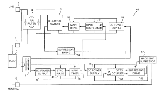
Referring now to Figure 4, there is illustrated therein
in block diagram form power saving circuitry 40 for reducing the
current supplied to a load 4, which may be a fluorescent lamp
assembly comprising a numb~r of separate fluorescent lamp
fixtures, with each lamp fixture including a conventional ballast
-- 1 0--
2159~38
circuit. Power saving circuitry 40 comprises a power circuit
having Bilateral Switch S, which preferably takes the form of
bilateral switch means Sa described with reference l:o Figure 1
above, connected in series between the line terminal 1 of an AC
power supply and the load terminal 2, load 4 being connected in
the usual way to the neutral terminal 3 of the AC power supply.
Bi 1 ateral Swi tch 5 has one termi nal connected to the 1 i ne
terminal 1 and its other terminal connected to the load terminal
2. A filter 6 to suppress radio frequency interference may be
inserted in series with each of the line and. load termlnals 1, 2.
Bilateral Switch means 5 is controlled by a control circuit
described below, having the voltage wave forms sho~.~n in Figure S.
The control circuit is powered by a multi-secondary
transformer 7 which is dri~en from line terminal 1 and neutral
terminal 2. Each secondar~ voltage of transformer 7 is rectified
and regulated by regulators 48, 53 and 55, to provlde floating DC
supplies for the control circuitry.
A zero-crossing detector Sync Pulse circult 49 produces a
synchronizing pulse SYNC B in phase with the AC mains A each
half-cycle as shown in Fig~ire 5. This pulse triggers the Main
Timer 50 which produces a square-wave pulse C of adjustable
pre-determined duration, wllich ls conducted by Opto-coupler Sl to
the Maln Drive 52. Maln Drive 52 drlves the gate of the FET
~ 2159538
device of Bilateral Switch S with a square-wave pulse E identical
to main pulse C as shown in Figure 5, causing the Bilateral
Switch 5 to conduct current to the load during a predetermined
initial portion of each half-cycle of the AC mains. The
resulting load voltage G is shown in Figure 5. Although this
causes a capacitive power f~ctor, this effect may be used to
compensate for the inductive power factor found in most
commerci al i nstal 1 ati ons ~
When the drive signal E from the Main Drive circuit 52
lû terminates, Bilateral Switc~l 5 ceases conducting, and the voltage
across load 4 drops rapidly. If allowed to continue unabated in
the case of an inductive lo~d, the voltage would drop to a
negative potential sufficiellt to damage the active devices in the
circuitry. This effect is known as the Back-EMF (Electromotive
Force) produced when current is suddenly interrupted in an
inductive load. To prevent this Back-EMF, or high momentary
reverse voltage, from appearing across load 4 at the point in
each half-cycle when the Bilateral Switch S ceases conducting as
a result of the termination of the drive signal from Main Drive
52, the power saving circuitry 40 includes a Back-EMF Suppressor
57 which dissipates the switch-off energy into the load, where it
adds to the efficiency of the entire circuit. Back-EMF
Suppressor 57 acts ~ike an "active" fly back diode which
suppresses transient voltages which occur as a result of
-12-
~ 21~g53~
switching off of current through an inductive load.
Back-EMF Suppressor 57 preferably comprises a bilateral
switch like that shown in FiglIre l. Suppressor Timing circuit 58
detects the onset of switch-o~ f and triggers Suppressor Drive 56,
5 which in turn applies a drivillg pulse D to the gate of the FET
device of Back-EMF Suppressor 57. This causes the FET device of
Back-EMF Suppressor 57 to conduct until the initiation of the
next main timing pulse C, thereby dissipating the energy caused
by switching off Bilateral Switch 5, through the load 4. In
10 other words, the Circuit 57 fun ctions as a load energy return
circuit that returns the load energy to the load immediately
following the opening of bilateral Switch 5. A8 a result, the
overall efficiency of the circuit is increased, by utilizing the
energy stored in the load to p~oduce useful work.
11 Main pulse C from Main Timer 50 is also connecte~ to the
l ight-emitting part of Opto-coupler 54, which produces 2nother
pulse F identical to pulse C ~hich disables Suppressor Drivr 56,
so that when Bilateral S~litch 5 is conducting, Back-EMF
15 Suppressor 57 is disabled. This prevents spurious noise signals
from act1vating Back-EMF Suppressor 57. During the interval wh~n
main pulse C is not active, Opto-coupler 54 is not active and
Suppressor Drive 56 is enabled to accept a trigger pulse.
It will be appreciated that the power saving circuitry of
20 the present invention need not. include Back-EMF Suppressor 57 and
its related circuitry if the power saving circuit is used m~rely
13
~ 21~9~38
to control the power output to resi sti ve 1 oads such as
incandescent lights connected to an AC source, because there is
no energy stored therein, unlike inductive loads.
The power output of power saving circuitry 40 is
proportional to the duratiorl of pulse C from Main Timer 50, which
is adjustable over a wide range. Dependlng upon the load used,
the power output can be ad jl~stable from almost 0' to almost lOO~o
of full power. In one embo~iment, the duration of main pulse C
is controlled by a potentiometer, which may be external to the
circuit, to allow for manual ad justment of the power level
delivered to the load. Alt~rnatively, the use of a
photosensitive resistor or thermally sensitive resistor in place
of the external potentiometer would allow the power delivered to
the load to be determined by light level or temperature. This
would enable automatic or feedback control of the output of the
load. For example, the photosensitive resistor could be made
operable to react to the aml~ient or outside light levels, thereby
increasing the power output level if the ambient light fell belo~
a certain level. Similarly, it would be possible to provide for
light level feedback to achieve a constant illumination level,
with the addition of a suitable light detector and associated
feedback circuitry.
Referring now to Fi~ures 6 and 7, there is disclosed
-- 1 4--
21~9S38
.
therein an alternative po~er saving circuit operable to place the
load current in the middle of each half-cycle of the AC po~er
supply, so as to result in a unity power factor. This
alternative embodiment of the power saving circuitry of the
present invention is operable to cause the bilateral switch means
to not start conducting current until after a predetermined
interval following the beginning of each alternate half-cycle.
Alternative power saving circuitry 60 i5 configured to
include Bilateral Switch 65 in the form of the bilateral switch
means shown in Figure 2 or Figure 3 comprising two unilateral
switches ~ and B, together with their associated drive circuits,
designated 72 and 84 in Figure 6. These drive circuits
correspond respectively to drive circuits 34, 33 of Figure 2 or
3. Because Bilateral Switch 65 includes two discrete switches,
circuitry 60 ~nust include two drive circuits, one to drive each
of the two switches. However, it should be appreciated that the
Bilateral Switch 5a (Figure 1) using only one FET device, could
as well be used as the Bilateral switch 65, in which case only
one drive circuit ~designated 52 in Figure 1) would be necessary.
The control circuit of po,ler saving circuitry 60 includes
a multi-secondary transformer 67, ~lith primary connected across
AC termi nal s 1 and 3, and a number of secondari es connected to
rectifiers and DC regulators to form DC power supplies 68, 73. 75
and 85. ~ero-crossing Detector 69 produces a sync pulse B in
phase with the AC mains A each half-cycle as shown in Figure 7.
Thi s pul se tri ggers Del ay Timer 79 to produce a square-wave pul se
_ 1 1
.
~ 2159~3~
C of ad justable duration, whi ch~ in turn triggers Main Timer 70.
Both Main Timer 70 and Delay Timer 79 are adjustable by means of
a single potentiometer in their timing networks. The
potentiometer is connected in such a way that the square-waYe
pul se D 1 asts for an equal amount of time both before and after
the maximum voltage point of each half-cycle of the AC power
supply. By altering the pot~ntiometer of Main Timer 70, the
length of the square wave pulse D as a proportion of the
half-cycle time can be varie~, with the midpoint of pulse D
always being at the midpoint of the length of the half-cycle.
The square-wave main pulse D of Main Timer 70 is
conducted by Opto-coupler 74 to disable the operation of Back-EMF
Suppressor 77 during the durdtion thereof, and as well, is
conducted to Inhibit circuit 80, which inhibits either Drive A
circuit 72 or Drive B circuit B4, depending upon the polarity of
the AC mains A. During the l1alf-cycle when the instantaneous
value of the AC mains voltage is posit1ve with respect to the
source of Switch A (which may be either FET device 25 shown in
Figure 2 or FET device 30 shown in Figure 3), the main pulse D is
conducted to Signal A circuit 81, which in turn relays the main
pulse D to Drive A circuit 72, via Opto-coupler 71. Meanwhile,
Signal B circuit 82 is disabled, by Inhibit circuit 80. Drive A
circuit 72 produces a square-wave pulse E identical to main pulse
D, whi ch i t feeds vi a a resi stor to the gate of Swi tch A, causi ng
- 1 6--
- -
~ 21~9~38
Switch A to conduct current t~o the load during the predetermined
interval when the main pulse is present.
Therefore, in operation, during the half-cycle of the AC
power supply when Switch A is being driven by Drive A circuit 72,
Switch A conducts for the predetermined time during which the
driving signal exists. This driving signal starts a
predetermined interval after the beginning of the half-cycle and
ends an equal predetermined interval before the end of the
half-cycle, so the conducting time is symmetrical with respect to
lO the middle of the half cycle.
The operation of Signal B circuit 82 is similar to that
of Signal A circuit 81, except that Signal B circuit 82 operates -~
during each alternate half-cycle of the AC mains. When actuated,
Signal B circuit 82 sends a signal the same duration as
square-wave slgnal D from Timer 70 to the light emitt1ng diode of
Opto-coupler 83. The light-sensitive element of Opto-coupler 83
in turn conducts the square-wave signal to Drive B circuit 84,
which produces a square-wave signal F at its output terminal
which is applied to the gzte of Switch B (which is either FET
20 device 26 if the circuit of Figure 2 is being used, or FET device
29 if the circuit of Flgure 3 is being used). Therefore, Switch
B conducts for the predetermined time during each half-cycle
during which the gate of Switch 8 is supplied with drive signal
-l 7-
2159538
F. Current therefore passes through Switch B and load 4 for such
predetermined time during each alternate half-cycle.
The resulting load v~lltage J is shown in Figure 7. Since
the AC power supply current passes through the load for an
ad justable middle portion of each half-cycle, by operation of
power saving circuitry 60, the voltage and current are in phase,
so there is no resulting reduction of power factor.
Back-EMF Suppressor 77 functions like previously
described Back-EMF Suppressor 57, to prevent a high momentary
reverse voltage from appearing across load 4 at the point in each
half-cycle when either Switch A or Switch B ceases conducting, in
the case of inductive loads.
Zero crossing Detector 69 preferably includes a brief
delay at start-up, e.g. 1 or 2 seconds, before producing sync
pulses B, thereby allowing ~oltage in other parts of the circuit
to stabilize before application of a drive signal to Bilateral
Switch 65. This delay is achieved by a timing capacitor, which
is discharged quickly when the AC power is interrupted, so that
the delay is obtained even after brief power failure or a quick
20 manual turn-off and turn-on peri od.
Main Timer 70 may also include a sensing means to detect
-18-
-
21S9538
the voltage level of the AC mains and to alter its output in such
a fashion as to compensate for fluctuations in the AC mains
voltage level. This insures a constant power to the load at the
same setting of the Main Timer 70 chosen prior to the fluctuation
of the AC mai ns.
Figures 8a and 8b are schematic diagrams of the circuitry
for the preferred embodiment of the power saving circuitry of the
present invention. This particular embodiment is operable to
conduct current from the power supply to the load for a
predetermjned time terminating at a predetermined interval before
the end of each alternate half-cycle. However, it can be easily
adapted to conduct current during a middle portion of each
half-cycle by inclusion of a delay timer as shown in Figure 6.
Referring first to Figure 8b, there is shown therein
timing control circuitry 9û which generates the timing signal to
operate the power devices used in the high voltage circuits shown
in Figure 8a. Transformer Tl has a primary side connected
between the line and neutral of the AC power source. It has
three secondaries, Tla, Tlb and Tlc, which are all 12v 60 H~ AC
sources, as indicated in Figure 8a. Tlc, together with transient
suppressor V2, bridge rectifier 8Rl, diode D6, capacitor C2, and
voltage regulator IC4, form a 12v DC power supply for the control
circuitry 90. Diode D6 isolates the power supply capacitor C2
1 9--
2159~38
from the rectified AC waveform 8 of Figure 9 which appears across
Rl .
Transistors Q4, Q6, alld Q7, diodes D10 and Dll, resistOrS
Rl, R3, R6, R7 and R14 form a pulse generator which produces a
synchronizing pulse SYNC C, at each zero-crossing of the AC power
line A. The negative going edge of this pulse is derived by a
network formed by C3, R9 and D7, and used to trigger the Main
Timer ICl.
At turn-on of the power, capacitor Cl is discharged, so
it inhibits the operation of the pulse generator through R8, D12
and Q7, with the result that no timing signals are generated for
the first few seconds of the application of power to the
switching devices. This ensur~es that the circuit begins operation
under controlled conditions r-lt the first zero-crossing of the AC
power after the time del ay ol one to two seconds. Capacitor Cl
charges through R2 and becomes inactive after the time delay
unless there is some interrul)tion of the AC power. If the
interruption is less than on~ cycle, the circuit continues to
function normally with no interruption of the control signals,
but if the interruption is l(~nger than one cycle, the regulated
power supply drops to almost zero and capacitor Cl discharges
through diode D8 in less tha~1 one cycle. When the power is
restored, the circuit functions as before with a brief start-up
-20-
21~9538
delay to ensure proper timing. This circuit helps to ensure
stable performance under fluctuating power conditions (i.e. a
lightning storm or electrical failure on an ad jacent service).
Main Timer ICI produces a signal MAIN E, synchronized to
trigger pulse SYNC C, whose duration is determined by timing
components resistor R13, potentiometer Pl and capacitor C4. The
power delivered by the switch devices to the load is proportiona
to the duration of the MAIN signal. Increasing the duration of
the MAIN signal E by increasing the value of potentiometer Pl
10 will proportionally increase the power delivered by the circuit
to the load, up to a maximum of roughly 95~ of full power, full
power being measured with no power saving circuit in place.
Timing network R13, Pl, and C4 is a power regulating
circuit referenced to the AC signal at bridge rectif jer BRl which
compensates for any fluctuations in the AC line level so as to
maintain a constant electrical power delivered to the load. For
example, if the duration of MAIN signal E was set to deliver a
fixed power level to the lo~d, and the line voltage dropped
because of some external falIlt, the voltage output at BRl would
20 proportionally drop, and the time to charge capacitor C4 would
increase. The MAIN signal ~ would then increase in duration,
providing a longer connecti~)n of the load to the line, whose
voltage had been reduced, resulting in a nearly constant power
-21 -
2159~38
.~
delivered to the load. Similarly, lf the line voltage were to
increase, the voltage at BRI would increase, caus~ng C4 to be
charged faster. The MAIN s ignal E would then decrease in
duration, providing a reduced connect10n of the load to the line,
whose voltage had been increased. Thus, a constant load power is
maintained under fluctuating line conditions.
Transi stor Q5 and resi stor R5 produce pul se RESET D,
which is an inverted version of the SYNC C pulse. The network
formed by C6, R10, and D9 derives the negative-going edge of this
pulse and activates the reset line of the Main Timer ICl. This
ensures that the Main Timer Pulse E does not extend beyond the
duration of one half-cycle of the AC line.
Transistor Q10, diodes D14 and D15, resistors R29, R3û
and R31, and capacitor Cl9 form another timing network. This
network has been provided for loads such as fluorescent lamps,
which require a "warm-up" period before efficient operation is
achieved, to allow start-up at nearly 100% of full power level,
and drop-down to the preset, reduced power level after the delay
period. Capacitor Cl9 is initially discharged, but charges
2~ slowly through R30 and R31 ~Intil it reaches the supply voltage of
12V DC after 15 to Z0 seconds. Use is made of the modulation
input of Main Timer ICl. T~lis input (pin 5) allows the timing
duration to be modified by the application of a bias current or
-22-
~-- 21~9~3~
voltage. Initially, Q10 conducts through the action ~f D14, R30
and Cl9. This causes a current to be applied through R29 to pin
5 of Main Timer ICl. This cl~rrent increases the duration of MAIN
signal E almost to the end ol the half-cycle for as long as Q10
conducts, causing the load tl) receive almost full power during
the delay or "warm-up'' period. As Cl9 charges, Q10 is slowly cut
off, so that after the delay period, the timing is set solely by
R13, Pl and C4. Capacitor C5 is used to stabilize the modulation
i nput.
The MAIN signal E is conducted to the drive circuits
through Rll and opto-coupler light-emitting diodes OPTO la and
OPTO 2a. These signals are received by light-sensitive
phototransistors OPTO lb and OPTO 2b shown in Figure 8a. --
Referring now to Figure 8a, the high voltage power and
drive circuitry comprises main switch circuitry 91 and Back-EMF
suppressor circuitry 92. Transformer secondaries Tla and Tlb
together with bridge rectifiers BR2 and BR3, capacitors C12 and
ClS, and integrated circuits ICS and IC6 form isolated 12V DC
regulated power supplies used to power main switch circuitry 91
and Back-EMF Suppressor circuitry 92.
Considering main switch circuitry 91 first, the MAIN
signal E is conducted from LED OPTO la of Control Circuit 90 to
-23-
~ 2159~8
phototransistor OPTO Ib and resistor R24 which send an inverted
versian of signal E to Main Drive IC2. This device provides
Schmitt Trigger action to suppress interference signals as well
as providing up to 200mA to drive to the capacitiYe gate of the
FET switches Ql and Q2. Resistor R25 and capacitors C17 and C18
are for stability. Main Drive IC2 inverts the signal again,
producing a pulse F identical to pulse E which drives the gates
of FET switches Ql and Q2. Resistors R26 and R27 1 imit the gate
current at switching and ~ener diodes Dl and 02 are used as
transient suppressors to protect the sensitive gates of FET
switches Ql and Q2. FETs are chosen for ~he ease of drive
circuitry, ease of paralleling for higher current, and low
on-resistance for low power dissipation. Although two
transistors in parallel are shown, any number of devices may be
used in parallel in this way to increase turrent ratings.
The power FETs Ql and Q2 are protected from high
transient pulses by varistor Vl and snubber network R28 and C8.
The FETs Ql and Q2 are used on the DC side of bridge rectifier
BR4 in the configuration sho~ln in Figure ~, in order that they
may conduct for both positive and negative halves of the AC
cycle. Alternatively, the configuration of Figure 2 or Figure 3
could be utilized instead of the one sho~n in Figure 1 (in which
case a second drive device would have to be included in the
circuit, as shown in Figure 6), although the configuration of
2159~i38
Figure 1 is preferred because it requires only one floating drive
c i r c u i t .
Inductors Lla and Llb and capacitor C9 form a radio
frequency interference (RFl) filter which suppresses the
transient voltage pulses which result from rapidly switching on
and off the power devices Ql and Q2. This network effectively
isolates the power saving circuit from other loads on the same AC
line. Ll conslsts of two bifilar windings a and b on a low
permeability, high-frequency, ferrite toroidal core. C9 is an AC
rated capacitor.
Main switch circuitry 91 described above is sufficient to
control the power output to a resistive-or incandescent load
connected to an AC source. HoweYer, in order to control
inductive or fluorescent loads, the additional suppressor
circuitry 92 shown in Figure 8a is requ~red, because large
transient voltages are generated across the switching devices and
the load, when switching inductive loads. These voltages
generate interference signals which disturb other equipment, and
which are potentially destructive to the switch devices and the
load. In AC circuits, a "flyback" diode cannot be used across =
the load as it would represent a short-circuit during each
alternate half-cycle of the AC line. The solution of this
problem requires a controlled short circuit across the load
-25-
21~53~
immediately following the turn off of the main switch device.
The energy stored in the load then circulates as current,
producing useful work in t~le load, and does not produce a
damaging high voltage pulse. FET device Q3 on the DC side of
bridge rectifier BRS provides this short circuit path across the
LOAD and NEUTRAL terminals. This circuit acts to suppress the
back-EMF at switching. It is desirable to activate suppressor
circuitry 92 at the point when the load voltage crosses zero
volts but before it builds up an appreciable negative potential
as shown by the dashed line on LOAD voltage G in Figure 9.
Several alternative ways ot triggering this circuit are feasible.
The suppressor could be activated whenever the Main Drive slgnal
is not applied. This woul(i create a potential short-circuit of
the LINE to NEUTRAL if eit~ler of the transistors Ql or Q3 was
slow to turn off. A short time delay may be inserted between the
end of the MAI~I signal E and the beginning of the Suppressor
Drive signal H. This delay would allow Ql and QZ to turn fully
off before the application of a drive signal to Q3. If, however,
the delay time is too long, or drifts after it has been set, the
load voltage may be allowed to switch to a dangerously high level
of opposite polarity. This alternative then, does not allow for
load or timing variations. The slope of the load voltage
waveform G may be sensed, as the turn-off portion of the waveform
is steepest. However, the voltage across the load at the
application of the suppressor ts left uncontrolled. For these
-26-
2~ 59538
reasons, voltage level sensing is preferred as a means of
feedback control for the suppressor, allowing the timing to be
varied automatically to suit the load characteristics.
The voltage divider formed by R14 and R15 senses the
rectified voltage level across the load. When the potential at
the junction of R14, RS an~ D14 drops below roughly lOV, Q9 and
Q8 turn on causing a trigger pulse through R18, Cll, Rl9 and D13.
This triggers Suppressor Driver/Timer IC3 which is configurated
in the same way as ICl. Driver/Timer IC3 produces a square-~ave
10 Suppressor Drive Signal H ~hose duration is determined by timing
network R20 and C13, and reset source OPTO 2b and R22. OPTû 2b
is a photo-sensitive dev1ce which detects the MAIN signal E and
produces a disable signal ,~ which disables the operation of IC3.
In this way, the Suppressol^ Drive signal H from IC3 cannot
overlap with the Main Driv~ signal F. The Suppressor Drive
signal H is supplied to the gate of FET switch Q3 through a
current-limiting resistor R21, with the sensitive gate protected
from transient voltages by zener diode D3. While one MOSFET
device Q3 is shown on the [)C side of bridge rectifier BR5,
20 several transistors connected in parallel as shown in the Main
Drive circuit may be used. In order to delay the voltage
transient caused at switch-off of the main devices, to allow a
small delay before the SupF)ressor Driver/Timer IC3 is activated,
a capacitor C10 is added in parallel with the load. This
-27-
2159~38
capacitor stores energy during the initial part of the cycle when
the Main Drive slgnal F is present and the line voltage is
supplied to the load. When the Main Drive signal F is removed,
the line voltage is disconnected and line current K ceases to
flow. The load current L is momentarily provided by the
capacitor C10 which discharges over a brief period until the
voltage drops sufficiently to trigger the Suppressor Driver/Timer
IC3. At this point, switch Q~ is activated and the load is
short-circuited until the beginning of the ne~t MAIN signal. The
load current L is then maintalned smoothly by the suppressor
current M, with no harmful transients at turn-off.
The resulting load current occurs in the initial part of
the half-cycle, thus presenting an apparent low, capacitive,
power factor to the 1 i ne. Thi s tends to bal ance any l o~l
inductive, power factor lcads in the installation to bring the
overall power factor closer to unity. If power factor correction
is not desired, the embodiment of Figures 6 and 7 may be used.
While the present invention has been described with
reference to various preferred and alternative embodiments, it is
to be understood that these embodiments are illustrative only,
and that the present invention is not limited thereto, but
includes all embodiments ~ithin the scope and spirit of the
appended cl aims.
-28-