Language selection

Search

Patent 2159558 Summary

Third-party information liability

Some of the information on this Web page has been provided by external sources. The Government of Canada is not responsible for the accuracy, reliability or currency of the information supplied by external sources. Users wishing to rely upon this information should consult directly with the source of the information. Content provided by external sources is not subject to official languages, privacy and accessibility requirements.

Claims and Abstract availability

Any discrepancies in the text and image of the Claims and Abstract are due to differing posting times. Text of the Claims and Abstract are posted:

  • At the time the application is open to public inspection;
  • At the time of issue of the patent (grant).
(12) Patent Application: (11) CA 2159558
(54) English Title: ELECTRONIC INTERLOCK FOR MULTIPLE PTO ENABLE SWITCHES
(54) French Title: VERROUILLAGE ELECTRONIQUE POUR COMMUTATEUR DE PRISE DE FORCE MULTIPLES
Status: Dead
Bibliographic Data
(51) International Patent Classification (IPC):
  • G05B 24/02 (2006.01)
  • B60K 25/00 (2006.01)
  • F02D 43/00 (2006.01)
(72) Inventors :
  • SWENSON, ERIC T. (United States of America)
  • THOMAS, RILEY A., III (United States of America)
  • BLANCHARD, RONALD L. (United States of America)
  • MARSHALL, BRIAN P. (United States of America)
(73) Owners :
  • NAVISTAR INTERNATIONAL TRANSPORTATION CORP. (United States of America)
(71) Applicants :
(74) Agent: FINLAYSON & SINGLEHURST
(74) Associate agent:
(45) Issued:
(22) Filed Date: 1995-09-29
(41) Open to Public Inspection: 1996-08-22
Examination requested: 2002-05-02
Availability of licence: N/A
(25) Language of filing: English

Patent Cooperation Treaty (PCT): No

(30) Application Priority Data:
Application No. Country/Territory Date
395,370 United States of America 1995-02-21

Abstracts

English Abstract


Multiple control-request switches are operatively
coupled by an electronic interlock circuit with an
electronic engine control that controls an engine that
powers a heavy duty automotive vehicle. The vehicle is
also equipped with one or more devices, such as an air-
compressor or hydraulic pump, that are powered from the
engine via a power take-off. The control-request switches
request control of this equipment from various stations
via control of an operational function of the engine,
such as control of engine speed. The interlock circuit
functions to allow only a first-to-be-actuated of the
control-request switches to acquire control so that
subsequent actuation of any other switch causes the
control to go to a default mode to avoid conflicting
control of the engine and equipment powered through a
power take-off.


Claims

Note: Claims are shown in the official language in which they were submitted.


What is claimed is:

1. In an internal combustion engine comprising an
electronic engine control for controlling various
operational functions of the engine, plural control-
enabling devices that are individually actuable for
enabling one operational function of the engine to occur,
and an interlock circuit for operatively coupling said
control-enabling devices with said electronic engine
control such that when one of said control-enabling
devices has been actuated to enable that one operational
function to occur, subsequent actuation of any of the
remainder of said control-enabling devices terminates the
enablement of that one operational function, the
improvement in said interlock circuit which comprises:
A) memory circuit means having plural inputs and
respective plural outputs and comprising memory for
giving and maintaining an output signal at a respective
output whenever an input signal is received at the
respective input;
B) plural input circuits respectively operatively
coupling respective ones of said control-enabling devices
with respective ones of said inputs of said memory
circuit means for providing respective input signals to
respective ones of said inputs;
C) validation circuit means having plural inputs and
an output means and comprising means for giving a
validation signal at said output means only in response
to any one of plural valid combinations of input signals
to said validation circuit means' inputs;
D) plural coupling circuits respectively operatively
coupling respective outputs of said memory circuit means
with respective inputs of said validation circuit means
for supplying respective output signals of said memory
circuit means to respective inputs of said validation
circuit means;
E) said validation circuit means comprising means
for giving a validation signal at its output means in

13

response to a first-to-be-actuated of said control-
enabling devices and means for terminating the validation
signal in response to a second-to-be-actuated of said
control-enabling devices; and
F) means operatively coupling said output means of
said validation circuit means with said electronic engine
control for enabling that one operational function of the
engine to occur when the validation signal is given and
for terminating the enablement of that one operational
function when the validation signal is terminated.

2. The improvement set forth in claim 1 wherein said
validation circuit means comprises a binary-to-decimal
converter circuit;
said inputs of said validation circuit means
comprise individual input terminals of said binary-to-
decimal converter circuit, each of which input terminals
is operatively connected with a respective output of said
memory circuit means and corresponds to a particular
binary digit of a binary number;
said output means of said validation circuit means
comprises individual output terminals of said binary-to-
decimal converter circuit, each of which output terminals
corresponds to a particular decimal digit; and
said means operatively coupling said output means
of said validation circuit means with said electronic
engine control comprises connections only with those
output terminals of said binary-to-decimal converter
circuit that correspond to valid combinations of input
signals to said input terminals of said binary-to-decimal
converter circuit.

3. The improvement set forth in claim 2 wherein said
means operatively coupling said output means of said
validation circuit means with said electronic engine
control further comprises logic circuit means having
input means and output means;

14

said connections only with those output terminals of
said binary-to-decimal converter circuit that correspond
to valid combinations of input signals to said input
terminals of said binary-to-decimal converter circuit
comprise connections to said input means of said logic
circuit means;
by-pass circuit means by-passing said memory circuit
means and said validation circuit means for operatively
coupling said input circuits directly with said input
means of said logic circuit means;
means operatively coupling said output means of said
logic circuit means with said electronic engine control;
and
said logic circuit means comprises means for passing
the validation signal to said electronic engine control
via said logic circuit means' output means provided that
said by-pass circuit means confirms to said logic circuit
means directly from a respective one of said input
circuits, the actuation of the respective control-
enabling device.

4. The improvement set forth in claim 3 wherein said
input means of said logic circuit means comprises two
input terminals;
said connections only with those output terminals of
said binary-to-decimal converter circuit that correspond
to valid combinations of input signals to said input
terminals of said binary-to-decimal converter circuit
comprise in the connections of those output terminals of
said binary-to-decimal converter circuit to said input
means of said logic circuit means, respective diodes to
one of said two input terminals of said logic circuit
means; and
said by-pass circuit means comprises respective
diodes coupling respective input circuits to the other of
said two input terminals of said logic circuit means.


5. The improvement set forth in claim 4 wherein said
output means of said logic circuit means comprises an
output terminal via which the validation signal is
passed;
said means operatively coupling said output means of
said logic circuit means with said electronic engine
control comprises an electronic switch having a principal
conduction path and a control input for rendering said
principal conduction path selectively operable to a first
conductivity condition and to a second conductivity
condition different from such first conductivity
condition;
means operatively connecting said control input with
said output terminal of said logic circuit means to place
said electronic switch under the control of said logic
circuit means;
said principal conduction path of said electronic
switch comprises two terminals;
means operatively connecting one of said two
terminals of said principal conduction path with said by-
pass circuit means such that said respective diodes of
said by-pass circuit means couple the respective input
circuits with said one of said two terminals of said
principal conduction path;
and means operatively connecting the other of said
two terminals of said principal conduction path with said
electronic engine control.

6. The improvement set forth in claim 1 wherein said
memory circuit means comprises a latch command terminal
for receiving a momentary latch command signal and means
for causing any input signal that is present at the
respective input of said memory circuit means at the time
of such momentary latch command signal to be latched in
the memory of said memory circuit means and said memory
circuit means to give and maintain an output signal at
the respective output of said memory circuit means;

16

each of said control-enabling devices comprises a
respective request switch that is selectively operable to
first and second switch conditions and when in the second
switch condition provides a respective input signal to a
respective input of said memory circuit means;
each of said input circuits further comprises a
respective timing circuit for giving a momentary latch
command signal when the respective request switch is
operated to and maintained in the second switch
condition; and
means operatively connecting said timing circuits
with said latch command terminal of said memory circuit
means for supplying a momentary latch command signal from
any respective one of said input circuits to said latch
command terminal to cause an input signal present at the
respective input of said memory circuit means to be given
and maintained at the respective output of said memory
circuit means.

7. The improvement set forth in claim 1 wherein said
means operatively coupling said output means of said
validation circuit means with said electronic engine
control further comprises logic circuit means having
input means and output means;
further including a by-pass circuit means that by-
passes said memory circuit means and said validation
circuit means for operatively coupling said input
circuits directly with said input means of said logic
circuit means;
means operatively coupling said output means of said
logic circuit means with said electronic engine control;
and
said logic circuit means comprises means for passing
the validation signal to said electronic engine control
via said logic circuit means' output means provided that
said by-pass circuit means confirms to said logic circuit
means directly from one of said input circuits, the

17

actuation of the respective control-enabling device.

8. The improvement set forth in claim 1 wherein said
electronic engine control comprises means for controlling
engine speed as one of said operational functions, and
said interlock circuit provides for enablement of control
of engine speed from a first-to-be-actuated of said
control-enabling devices by enabling control when only
the first-to-be-actuated of said control-enabling devices
is actuated to give a respective input signal to the
respective input of said memory circuit means and by
terminating the enablement of control when a second-to-
be-actuated of said control-enabling devices is actuated
to cause said memory means to give an output signal at
more than one of its outputs.

9. In an internal combustion engine comprising an
electronic engine control for controlling various
operational functions of the engine, plural request
switches that are individually actuable for enabling one
operational function of the engine to occur, and an
interlock circuit for operatively coupling said request
switches with said electronic engine control such that
when one of said request switches has been actuated to
enable that one operational function to-occur, subsequent
actuation of any of the remainder of said request
switches terminates the enablement of that one
operational function, the improvement in said interlock
circuit which comprises:
A) request-switch-actuation-detection circuit means
having inputs and outputs and comprising means for
detecting actuation of each of said request switches and
for providing at a respective output a respective output
signal representing actuation of the respective request
switch;
B) plural coupling circuits respectively operatively
coupling respective ones of said request switches with

18

respective inputs of said request-switch-actuation-
detection circuit means for supplying respective input
signals to respective inputs of said request-switch-
actuation-detection circuit means;
C) validation circuit means comprising a binary-to-
decimal converter circuit means that comprises individual
inputs, each of which inputs is operatively connected
with a respective output of said request-switch-
actuation-detection circuit means and corresponds to a
particular binary digit of a binary number;
D) said binary-to-decimal converter circuit means
further comprising individual outputs each of which
corresponds to a particular decimal number; and
E) means operatively coupling said electronic engine
control only with certain outputs of said binary-to-
decimal converter circuit means for enabling the one
operational function to occur only when a valid input
signal pattern is present at said inputs of said binary-
to-decimal converter circuit;
F) each respective valid input signal pattern
causing a respective validation signal to appear only at
a single respective one of said certain outputs of said
binary-to-decimal converter circuit means.

10. The improvement set forth in claim 9 wherein
said binary-to-decimal converter circuit means comprises
means for terminating the enablement of that one
operational function when a valid input signal pattern
appears at more than one of said certain outputs.

11. An interlock circuit for operatively coupling
plural control-enabling devices that are individually
actuable for causing the interlock circuit to give an
enabling signal when one of said control-enabling devices
has been actuated and to terminate the enabling signal
upon subsequent actuation of any of the remainder of said
control-enabling devices, said interlock circuit

19

comprising in combination with said control-enabling
devices:
A) memory circuit means having plural inputs and
respective plural outputs and comprising memory for
giving and maintaining an output signal at a respective
output whenever an input signal is received at the
respective input;
B) plural input circuits respectively operatively
coupling respective ones of said control devices with
respective ones of said inputs of said memory circuit
means for providing respective input signals to
respective ones of said inputs;
C) validation circuit means having plural inputs and
an output means and comprising means for giving a
validation signal at said output means only in response
to any one of plural valid combinations of input signals
to said validation circuit means' inputs;
D) plural coupling circuits respectively operatively
coupling respective outputs of said memory circuit means
with respective inputs of said validation circuit means
for supplying respective output signals of said memory
circuit means to respective inputs of said validation
circuit means;
E) said validation circuit means comprising means
for giving a validation signal at its output means in
response to a first-to-be-actuated of said control-
enabling devices and means for terminating the validation
signal in response to a second-to-be-actuated of said
control-enabling devices; and
F) means operatively coupled with said output means
of said validation circuit means for giving the enabling
signal when the validation signal is given and for
terminating the enabling signal when the validation
signal is terminated.

12. An interlock circuit as set forth in claim 11
wherein said validation circuit means comprises a binary-


to-decimal converter circuit;
said inputs of said validation circuit means
comprise individual input terminals of said binary-to-
decimal converter circuit, each of which input terminals
is operatively connected with a respective output of said
memory circuit means and corresponds to a particular
binary digit of a binary number;
said output means of said validation circuit means
comprises individual output terminals of said binary-to-
decimal converter circuit, each of which output terminals
corresponds to a particular decimal digit; and
said means operatively coupled with said output
means of said validation circuit means comprises
connections only with those output terminals of said
binary-to-decimal converter circuit that correspond to
valid combinations of input signals to said input
terminals of said binary-to-decimal converter circuit.

13. An interlock circuit as set forth in claim 12
wherein said means operatively coupled with said output
means of said validation circuit means further comprises
logic circuit means having input means and output means;
said connections only with those output terminals of
said binary-to-decimal converter circuit that correspond
to valid combinations of input signals to said input
terminals of said binary-to-decimal converter circuit
comprise connections to said input means of said logic
circuit means;
by-pass circuit means by-passing said memory circuit
means and said validation circuit means for operatively
coupling said input circuits directly with said input
means of said logic circuit means; and
said logic circuit means comprises means for passing
the validation signal to said logic circuit means' output
means to give the enabling signal at said logic circuit
means' output means, provided that said by-pass circuit
means confirms to said logic circuit means directly from

21

a respective one of said input circuits, the actuation of
the respective control-enabling device.

14. An interlock circuit as set forth in claim 13
wherein said input means of said logic circuit means
comprises two input terminals;
said connections only with those output terminals of
said binary-to-decimal converter circuit that correspond
to valid combinations of input signals to said input
terminals of said binary-to-decimal converter circuit
comprise in the connections of those output terminals of
said binary-to-decimal converter circuit to said input
means of said logic circuit means, respective diodes to
one of said two input terminals of said logic circuit
means; and
said by-pass circuit means comprises respective
diodes coupling respective input circuits to the other of
said two input terminals of said logic circuit means.

15. An interlock circuit as set forth in claim 14
wherein said output means of said logic circuit means
comprises an output terminal via which the enabling
signal is given;
further including an electronic switch having a
principal conduction path and a control input for
rendering said principal conduction path selectively
operable to a first conductivity condition and to a
second conductivity condition different from such first
conductivity condition;
means operatively connecting said control input with
said output terminal of said logic circuit means to place
said electronic switch under the control of said logic
circuit means;
said principal conduction path of said electronic
switch comprises two terminals; and
means operatively connecting one of said two
terminals of said principal conduction path with said by-

22

pass circuit means such that said respective diodes of
said by-pass circuit means couple the respective input
circuits with said one of said two terminals of said
principal conduction path.
16. An interlock circuit as set forth in claim 11
wherein said memory circuit means comprises a latch
command terminal for receiving a momentary latch command
signal and means for causing any input signal that is
present at the respective input of said memory circuit
means at the time of such momentary latch command signal
to be latched in the memory of said memory circuit means
and said memory circuit means to give and maintain an
output signal at the respective output of said memory
circuit means;
each of said control-enabling devices comprises a
respective request switch that is selectively operable to
first and second switch conditions and when in the second
switch condition provides a respective input signal to a
respective input of said memory circuit means;
each of said input circuits further comprises a
respective timing circuit for giving a momentary latch
command signal when the respective request switch is
operated to and maintained in the second switch
condition; and
means operatively connecting said timing circuits
with said latch command terminal of said memory circuit
means for supplying a momentary latch command signal from
any respective one of said input circuits to said latch
command terminal to cause an input signal present at the
respective input of said memory circuit means to be given
and maintained at the respective output of said memory
circuit means.

17. An interlock circuit as set forth in claim 11
wherein said means operatively coupled with said output
means of said validation circuit means further comprises
logic circuit means having input means and output means;

23

further including a by-pass circuit means that by-
passes said memory circuit means and said validation
circuit means for operatively coupling said input
circuits directly with said input means of said logic
circuit means; and
said logic circuit means comprises means for passing
the validation signal to said logic circuit means' output
means to give the enabling signal at said logic circuit
means' output means, provided that said by-pass circuit
means confirms to said logic circuit means directly from
one of said input circuits, the actuation of the
respective control-enabling device.

18. An interlock circuit as set forth in claim 11
wherein said control-enabling devices are switches.

24

Description

Note: Descriptions are shown in the official language in which they were submitted.


~1S~558
~" .
- D-4684


~LECTRONIC INTERLOCR FOR MULTIPLE PTO ENABLE SWITCHES
FIELD OF THE INVENTION
This invention relates generally to electronic
controls for engines and more especially to an electronic
interlock circuit for interlocking control-request
switches, each of which is capable of enabling an
associated control to control an operational function of
the engine, such that conflicting control of the
operational function is avoided, and/or for interlocking
switches, each of which is capable of enabling an
associated control to control the operation of one or
more various pieces of equipment or machinery powered
from the engine via one or more power take-offs, such
that conflicting control of the equipment or machinery is
avoided.
CROSS-REFERENCE TO RELATED APPLICATION
The inventors' commonly assigned application "Single
Switch PTO Enabler", Ser. No. , filed
, (Assignee's Docket No. D-4675) is hereby
referenced.
BACKGROUND AND SUMMARY OF THE INVENTION
Electronic engine controls comprise electronic
circuitry, typically microprocessor based, that processes
various inputs to provide the desired engine control
functions. Usage of electronic engine controls has become
commonplace in internal combustion engines that power
automotive vehicles.
Certain engine-powered vehicles have one or more
PTO's (power take-offs) for allowing equipment or
machinery other than the vehicle itself to be operated by
the engine, and such vehicles require an associated
control for controlling engine operation, engine speed
for example, when a PTO is in use operating a piece of
equipment. If the associated control has multiple control
stations, and/or if multiple pieces of equipment are to
be controlled, it is desirable to minimize the risk that

2~9S~

conflicting inputs from the associated control resulting
from human operator error or inadvertence will affect
engine and/or equipment operation. Accordingly, it has
heretofore been known to provide equipment interlocks
using electromechanical relay circuits that give control
priority to a request for control from a first-to-be-
actuated of multiple control-request switches. (These
control-request switches may sometimes hereinafter also
be referred to as control-enable switches.) If a second-
to-be-actuated of the multiple control-request switches
requests control before the request from the first-to-be-
actuated control-request switch has been withdrawn, the
request from the second-to-be-actuated control-request
switch will be denied. The same will be true for any
other control-request switch so long as the first-to-be-
actuated control-request switch retains control.
The present invention relates to a new and useful
interlock circuit that prevents associated controls from
commanding potentially conflicting operation of an engine
and/or of equipment that is powered from the engine
through one or more power take-offs. One important
advantage of the invention is that fewer relays are used
than in the prior relay-type interlock, and this in turn
means that wiring complexity is reduced because there are
fewer circuits and wiring connections. Reductions of this
nature can improve productivity and reliablity. The
invention is intended to assist in guarding against human
operator error that might otherwise cause potentially
conflicting requests to be given to the engine and/or
equipment powered from the engine via a PTO.
Briefly, the present invention may in one way
generally be described as an interlock circuit that
detects actuation of various control-request switches and
enables control by the first-to-be-actuated of multiple
control-request switches. Subsequent actuation of a
second-to-be-actuated control-request switch terminates
the enablement of control, which is accompanied by the

21~9S58

engine going to a default mode of operation (shut-down or
idle are possibilities depending upon how the default is
programmed into the engine control) and/or shutting down
and locking out equipment powered by the engine.
The invention is further characterized by a unique
organization and arrangement of standard electronic
circuit components that provide an electronic interlock
circuit between the control-request switches and the
electronic engine control. The circuit is powered by
available electric power, typically 12VDC.
The foregoing, along with further features,
advantages, and benefits of the invention, will be seen
in the ensuing description and claims, which are
accompanied by drawings. The drawings disclose a
presently preferred embodiment of the invention according
to the best mode contemplated at this time for carrying
out the invention.
BRIEF DESCRIPTION OF THE DRAWINGS
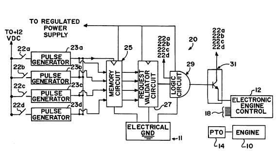
Fig. 1 is a general electrical schematic block
diagram of the inventive interlock circuit in association
with an engine having an electronic engine control.
Fig. 2 is a more detailed schematic electric circuit
diagram of the interlock circuit.
Figs. 3A and 3B are voltage waveforms useful in
understanding the operation of a portion of the circuit
shown in Fig. 2.
DESCRIPTION OF THE PREFERRED EMBODIMENT
Fig. 1 shows an exemplary application of the
inventive principles to a vehicle, such as a heavy truck,
that comprises an engine 10 that is controlled by an
electronic engine control 12. Engine 10 is typically a
diesel engine, but broader principles of the invention,
as applied to an engine, are not limited to any
particular application of the engine or type of engine.
Engine 10 operates the vehicle through a powertrain that
is not shown in the drawings; however, a PTO 14 is shown
in association with engine 10 since the invention relates

21~9~58

to certain requirements of engine control 12 for enabling
control over equipment (not shown) operated by the engine
via PT0 14.
PTO's per se are well known, and PT0 14 is a known
commercially available device that has mechanical
controls, such as a clutch (not shown) which connects the
engine 10 to the PTO for operation.
Engine control 12 receives a number of inputs, shown
generally at 18, processes the information received at
these inputs, and issues appropriate commands for
controlling engine 10. Details of how engine 10 is
controlled by control 12 generally do not relate to the
principles of the invention, except to the extent that
the particular engine control strategy that is shown here
by example requires an enabling signal input for enabling
control of a particular operational function of the
engine that affects the operation of a device (not shown)
driven by the PTO 14. In the present example, the
particular control strategy requires such an enabling
signal input in order to change the engine speed demanded
for operating a piece of equipment operatively coupled
with engine 12 via PTO 14.
Fig. 1 further shows the general organization and
arrangement of an interlock circuit 20 according to the
present invention. Circuit 20 operatively couples
multiple engine control-request switches with engine
control 12. Four such engine control-request switches are
shown by way of example, 22a, 22b, 22c, 22d, and each is
selectively actuable to provide, when actuated, a
control-request input signal to a respective pulse
generator circuit, 23a, 23b, 23c, 23d. Circuit 20 further
comprises: a memory circuit 25 having respective inputs
connected to respective outputs of the pulse generator
circuits; a request validator circuit 27 having
respective inputs connected to respective outputs of
memory circuit 25; a logic circuit 29 connected to sense
actuation of switches 22a, 22b, 22c, 22d and the output

2~59558

of request validator circuit 27; and an enable switch 31
that operatively couples circuit 20 with engine control
12. The existing negative-ground 12-volt DC electric
power source of the vehicle supplies electric power for
circuit 20. Further detail of circuit 20 is shown in Fig.
2 to which attention is now directed.
Each pulse generator circuit 23a, 23b, 23c, 23d
embodies certain aspects of the invention disclosed in
the above-referenced patent application "Single Switch
PTO Enabler", and further detail may be obtained
therefrom. Generally, each pulse generator outputs a
momentary switch function in the form of an electrical
pulse when the respective switch 22a, 22b, 22c, 22d is
actuated. Since each of the pulse generator circuits is
identical, only circuit 23a will be described, and it is
understood that the description applies to the other
three as well even though the drawing shows unique
reference signs for the individual circuit components of
each pulse generator circuit.
Circuit 23a comprises a timing circuit that acts on
the input signal that is given by the operation of switch
22a to closed condition. The timing circuit may be
considered to comprise: a series RC circuit composed of a
resistor R6 and a capacitor C5 connected in series; a PNP
transistor Q2; and resistors R10, R14, R18. Additional
components associated with the timing circuit are: diodes
D2, D6, D10; a capacitor Cl; a resistor R2; and a zener
diode Z2.
Resistor R2, zener diode Z2, and diode D2 form a
circuit that reduces the voltage that is received from
switch 22a when the switch is actuated. The voltage is
reduced to a suitable level for the particular memory
circuit 25 and logic circuit 29, and the timing circuit
components are chosen to also use this reduced voltage
for the timing circuit's power supply. The purpose of
capacitor Cl is essentially a noise filter, while diode
D2 blocks reverse current flow from the timing circuit

21~S9~5~

back toward the zener diode and the switch.
Resistor R6 and capacitor C5 form a series RC
circuit. The emitter terminal of transistor Q2 is
connected in common with the cathode of diode D2 and
terminals of resistors R6, R18, as shown. The
transistor's base terminal is connected through resistor
R10 in common with the commonly connected terminals of
resistor R6 and capacitor C5. The transistor's collector
terminal is connected through resistor R14 to ground
while the terminal of resistor R18 that is not connected
to the transistor's emitter terminal is also connected to
ground.
The pulse generator circuit operates in the
following manner. With switch 22a open, no voltage is
applied to the timing circuit; consequently transistor Q2
cannot be forward biased to a conductive state and so it
remains non-conductive. When switch 22a is operated from
open to closed, the reduced DC voltage of zener diode Z2
is applied through diode D2. Since capacitor C5 is
initially uncharged, closure of switch 22a causes current
flow through resistor R2, diode D2, and resistor R6 to
begin charging capacitor C5. Concurrent with this action,
transistor Q2 becomes forward biased into conduction so
that its emitter-collector path carries current through
resistor R14. Fig. 3B depicts this switching on a non-
dimensional scale, and it is this switching that
represents the beginning of an output pulse at the output
of pulse generator circuit 23a.
The series RC circuit executes an exponential
transient with the voltage across capacitor C5 becoming
increasingly positive. This is depicted in Fig. 3A. After
a certain portion of the transient has been executed, the
base current to transistor Q2 has decreased to a level
that is insufficient to maintain conduction through
transistor's emitter-collector path and so the transistor
switches from conduction back to non-conduction. This
represents the termination of the pulse and is also

2159~8

depicted in Fig. 3B.
When switch 22a is re-opened, capacitor C5 begins to
discharge through resistors R6, R18. The current flow
through resistor R18 reverse biases the base-emitter
junction of the transistor so that it is maintained non-
conductive. Eventually capacitor C5 is fully discharged
so that the circuit assumes its initial condition that
existed before switch 22a was first closed.
It is to be noted that switch 22a must remain closed
for at least as long as the required pulse width of the
output pulse, and in fact the switch can remain closed
for an indefinite amount of time thereafter before being
reopened. So long as switch 22a remains closed for at
least the minimum amount of time required for the pulse
width, the total amount of time that switch 22a remains
closed is not significant.
Memory circuit 25 is a standard integrated circuit
that has multiple input terminals 25a-25d and respective
multiple output terminals 25e-25h. It also has a latch
command terminal 25i. The circuit is also sometimes
referred to as a transparent latch circuit. Memory
circuit 25 operates in the following manner. Whenever a
latch command signal (in the form of a pulse produced by
one of the circuits 23a-23d) is supplied to terminal 25i,
an input signal at a respective input terminal 25a-25d is
latched in memory and to cause a respective output signal
to be given and maintained at the respective output
terminal 25e-25h after the latch command signal
terminates.
Each respective input terminal 25a-25d is connected
to the cathode terminal of the respective diodes D2-D5
such that when the respective switch 22a-22d is operated
closed, the reduced positive voltage indicative of switch
closure is delivered to the respective terminal 25a-25d.
Latch command terminal 25i is connected to the cathodes
of all four of diodes D10-D13. Since closure of a
respective switch 22a-22d also causes the respective

21~9~S8

pulse generator circuit 23a-23d to generate a momentary
output pulse, a control request from any switch 22a-22d
will additionally result in the application of a pulse
signal to latch command terminal 25i.
Hence, a first-to-be-actuated of request switches
22a-22d causes an output signal to appear at the
respective output terminal 25e-25h of memory circuit 25
while the remaining three output terminals of the memory
circuit give no output signal.
Request validator circuit 27 is a standard
integrated circuit that has multiple input terminals 27a-
27d and multiple output terminals, including the
illustrated output terminals 27e-27h. The specific
circuit employed in the present embodiment of the
invention is a binary-to-decimal decoder circuit in which
each of the respective input terminals 27a-27d
corresponds to a particular binary digit of a four digit
binary number. The circuit also has ten output terminals
tfour of which are terminals 27e-27h), each of which
corresponds to a respective decimal digit (i.e. 0-9).
When no signals are present at any of the input terminals
27a-27d (representing the binary number zero), no signals
are present at any of the ten output terminals
(representing the decimal number zero). Output terminal
27e represents the decimal number one; output terminal
27f, the decimal number two; output terminal 27g
represents the decimal number four; and output terminal
27h, the decimal number eight. Accordingly, when the
binary number "0001" is present at input terminals 27a-
27d, a signal is given at output terminal 27e; when the
binary number "0010" is present at input terminals 27a-
27d, a signal is given at output terminal 27f; when the
binary number "0100" is present at input terminals 27a-
27d, a signal is given at output terminal 27g; and when
the binary number "1000" is present at input terminals
27a-27d, a signal is given at output terminal 27h. It is
to be noted that each of these four particular numbers

21 ~9~5~

comprises only a single "1" binary digit (representing
the presence of a signal) while the remaining three
binary digits are all "O" (representing the absence of
signals). These are the only signal patterns that the
request validator circuit will recognize as valid signal
patterns.
If a non-zero binary number other than these four
particular ones is present at input terminals 27a-27d,
then a signal will be given at the corresponding output
terminal other than the four terminals 27e-27h. Such
other binary number will comprise more than multiple
"l's" as its binary digits, and so the output terminals
of the request validator circuit that provide respective
signals in response to these respective patterns having
more than a single "1" as one of its binary digits are
not connected in the instant interlock circuit.
Each of the respective output terminals 25e-25h of
memory circuit 25 is connected with a respective terminal
27a-27d of request validator circuit 27. The four output
terminals 27e-27h are coupled through respective diodes
D14, D15, D16, D17 whose cathodes are connected in
common. Consequently, a signal will appear at these
common cathodes only when a valid signal pattern is
present at the inputs of request validator circuit 27.
Logic circuit 29 may be considered essentially as a
two-input AND logic gate. The commonly connected cathodes
of diodes D14-D17 are connected to one input terminal 29a
of logic circuit 29. The cathodes of diodes D6, D7, D8,
and D9 are connected in common to the other input
terminal 29b. The anodes of the respective diodes D14-D17
are connected to the cathodes of the respective diodes
D2-D5 so that when any of the switches 22a-22d is closed,
a respective signal will be transmitted to input terminal
29b.
Logic circuit 29 further has an output terminal 29c
that gives an output signal when signals are present at
both input terminals 29a, 29b. Terminal 29c is connected

21~95S8

to the base terminal of an NPN transistor Q6 whose
collector terminal is connected to the commonly connected
cathodes of diodes D6-D9. The transistor's emitter
terminal is connected to the engine control to provide
the enable signal as a consequence of any of the valid
inputs to circuit 27.
With the foregoing description in mind, the
operation of the interlock circuit can now be more fully
explained. A first-to-be-actuated of control-request
switches 22a-22d will cause a "1" to be latched in memory
of memory circuit 25 so that a "1" appears at the
respective output terminal. This will create a valid
input signal pattern to circuit 27 which validates the
request for control that has been made by the first-to-
be-actuated of the control-request switches 22a-22d by
supplying a validation signal to input terminal 29a of
logic circuit 29. That a control request has been made is
confirmed by a signal also appearing at the other input
terminal 29b of the logic circuit, and so an enabling
signal is supplied by output terminal 29c of logic
circuit 29. Actuation of a control-request switch also
supplies voltage to the collector terminal of transistor
Q2 so that transistor Q2 switches to conduction to supply
an enable signal to the engine control allowing the
control associated with the first-to-be-actuated control-
request switch to acquire control.
If any other control-request switch is actuated,
while the control associated with the first-to-be-
actuated control-request switch continues to have
control, an invalid signal pattern will be stored in
memory circuit 25 and transmitted to request validator
circuit 27. Since an invalid pattern is now presented to
circuit 27, the output signal from circuit 27 will appear
at other than terminals 27e-27h, and a signal will cease
to be supplied to terminal 29a of logic circuit 29.
Consequently, the logic circuit will cease to provide
sufficient base current for transistor Q6, and the


21~95~

transistor will switch to non-conduction thereby
terminating the enable signal to the engine control. The
engine control will then be caused to operate to a
default mode since conflicting requests for control have
been issued. Before a control request can again be
validated, all of the control-request switches 22a-22d
must be opened.
Fig. 2 shows a regulated power supply RPS that
isolates the interlock circuit from the +12VDC vehicle
power supply but obtains power from the vehicle power
supply to deliver regulated voltage of suitable magnitude
for operating memory circuit 25, request validator
circuit 27 and logic circuit 29. While Fig. 2 shows the
collector of transistor Q6 connected to receive the
reduced voltage when any of the switches 22a-22d is
actuated, this is to satisfy particular requirements for
the particular engine control. If the engine control
enable were to require a +12 VDC signal, then the
collector of transistor Q2 could be connected directly to
the load side of each of the switches 22a-22d.
While the present disclosure of the inventive
principles enables the skilled person to utilize
conventional circuit design principles to fabricate
different designs for satisfying various timing needs,
the following components have been utilized in the
disclosed embodiment.
Resistor R1: 470 Ohms, 1/2 watt
Resistors R2-R5: 1.2 kOhms
Resistors R6-R9: 10 kOhms
Resistors R10-R13: 1.2 kOhms
Resistors R14-R17: 3.3 megOhms
Resistors R18-R21: 1.2 kOhms
Diodes D1-D17: lN4004
Zener Diodes Z1-Z5: lN4746A
Transistor Q1: TIP 31C
Transistors Q2-Q5: 2N4403
Transistor Q6: 2N2222

21S9558

Capacitors C1-C4: 1 microfarad
Capacitors C5-C8: 1 microfarad, 35v ceramic
Memory 25: Motorola MC14042Bd
Request Validator 27: Motorola MC14028Bd
Logic Circuit 29: Motorola MC14081Bd
Typical uses of the invention are in heavy duty
automotive vehicles on which additional power equipment
has been installed, including, but not limited to, air
compressors, hydraulic pumps, and equipment that can in
turn be operated from them, such as cranes, augers, and
booms. Where operation of a compressor or pump requires
control over engine speed, and where a vehicle has
multiple stations that can request such control, the
invention helps to guard against human operator error or
inadvertence that might otherwise give conflicting speed
signals.
While a presently preferred embodiment of the
invention has been illustrated and described, it is to be
appreciated that the principles may be practiced in other
equivalent ways within the scope of the following claims.

Representative Drawing
A single figure which represents the drawing illustrating the invention.
Administrative Status

For a clearer understanding of the status of the application/patent presented on this page, the site Disclaimer , as well as the definitions for Patent , Administrative Status , Maintenance Fee  and Payment History  should be consulted.

Administrative Status

Title Date
Forecasted Issue Date Unavailable
(22) Filed 1995-09-29
(41) Open to Public Inspection 1996-08-22
Examination Requested 2002-05-02
Dead Application 2005-09-29

Abandonment History

Abandonment Date Reason Reinstatement Date
2004-09-29 FAILURE TO PAY APPLICATION MAINTENANCE FEE
2004-11-01 R30(2) - Failure to Respond

Payment History

Fee Type Anniversary Year Due Date Amount Paid Paid Date
Application Fee $0.00 1995-09-29
Registration of a document - section 124 $0.00 1995-12-14
Maintenance Fee - Application - New Act 2 1997-09-29 $100.00 1997-09-17
Maintenance Fee - Application - New Act 3 1998-09-29 $100.00 1998-09-16
Maintenance Fee - Application - New Act 4 1999-09-29 $100.00 1999-06-21
Maintenance Fee - Application - New Act 5 2000-09-29 $150.00 2000-07-07
Maintenance Fee - Application - New Act 6 2001-10-01 $150.00 2001-06-27
Request for Examination $400.00 2002-05-02
Maintenance Fee - Application - New Act 7 2002-09-30 $150.00 2002-06-25
Maintenance Fee - Application - New Act 8 2003-09-29 $150.00 2003-06-26
Owners on Record

Note: Records showing the ownership history in alphabetical order.

Current Owners on Record
NAVISTAR INTERNATIONAL TRANSPORTATION CORP.
Past Owners on Record
BLANCHARD, RONALD L.
MARSHALL, BRIAN P.
SWENSON, ERIC T.
THOMAS, RILEY A., III
Past Owners that do not appear in the "Owners on Record" listing will appear in other documentation within the application.
Documents

To view selected files, please enter reCAPTCHA code :


To view images, click a link in the Document Description column. To download the documents, select one or more checkboxes in the first column and then click the "Download Selected in PDF format (Zip Archive)" or the "Download Selected as Single PDF" button.

List of published and non-published patent-specific documents on the CPD .

If you have any difficulty accessing content, you can call the Client Service Centre at 1-866-997-1936 or send them an e-mail at CIPO Client Service Centre.


Document
Description 
Date
(yyyy-mm-dd) 
Number of pages   Size of Image (KB) 
Representative Drawing 1998-01-22 1 15
Cover Page 1995-09-29 1 19
Abstract 1995-09-29 1 25
Description 1995-09-29 12 554
Claims 1995-09-29 12 522
Drawings 1995-09-29 2 54
Assignment 1995-09-29 11 590
Prosecution-Amendment 2002-05-02 1 44
Prosecution-Amendment 2004-04-30 1 28