Note: Descriptions are shown in the official language in which they were submitted.
'_, 21$99S3
METHOD OF AND APPARATU~ FOR IMPROVED DYNAMIC RANDOM
ACCE~ MEMORY (DRAM) PROVIDING INCREA~ED DATA BANDWIDTH
AND ADDRE~ING RANGE FOR CURRENT DRAM DEVICE~ AND/OR
EQUIVALENT BANDWIDTH AND ADDRE~ING RANGE FOR ~MALLER DRAM
DEVICE~
The present invention relates to dynamic random
access memory (DRAM) devices operating in either asynchro-
nous or synchronous modes, being more particularly con-
cerned with the increasing of the data bandwidth and
addressing range of current DRA~ devices, and/or providing
equivalent bandwidth and addressing range thereof for
smaller devices -- the invention attaining such results
with a radically new and different interface and associat-
ed access mechanism than conventionally used with DRAM
systems.
Bac~ground of Invention
In earlier days, the primary means for storing data
in computer, microprocessor and similar systems, resided
in a transistor-based high speed circuit that stored each
-2- 21 599~3
bit of information -- a so-called static random access
memory device, termed ~RAM, summarily described, for
example, on page 295-300 of a catalog of ~amsung
Electronics entitled M0~ Memory, 1993/94. A ~amsung Type
K~644002 cmos ~RAM, for example, was presented in a 32-pin
plastic unit (400 mil) providing 1,048,576 words by 4 bits
and using four common inpue and output lines and an output
enable pin operating faster than the address access time
ac read cycle -- the fast access times ranging from 15 to
25 ns. In order uniquely to select one of the over 1
million locations, 20 address bits are rejoined (20 of the
pins being address pins) along with 4 data pins and
control signals.
In an effort to meet increased RAM requirements, the
concept was evolved of storing each bit in a small
capacitor on the silicon unit or die, the integration of a
large number of capacitors taking far less space than
transistors -- so-called dynamic random access memory or
DRAM units. The resulting advantages of the DRAM unit in
increased storage capacity, higher data bandwidth and
savings in terms of device size, board space, power
consumption and cost, particularly when large numbers of
21S9953
-3-
such devices are implemented in a design, outweighed the
necessity for periodic charging of capacitors, and more
complex access mechanisms and control circuits; and DRAM
became one of the most, if not the most, popular type of ~-
memory.
The external circuit interface of the DRAM, moreover,
differs significantly from the ~RAM. Contrasting the
illustrative ~amsung Type K'.~644002 ~2AM above-described,
with a corresponding ~amsung Type KM44ClOOOB CM0~ DRAM, as
described on pages 330-337 of said ~amsung catalog, the
addressing is similar to uniquely identifying an element
within a matrix, with each location in the address space
being accessed by providing a row address and a column
address. For the 1 million x 4 bit example, only a total
of 20 address bits are required, 10 bits used to select
the row in which the bit is located and 10 bits selecting
the column of the desired bit in the selected row. As
compared with the ~aAM device only 10 address pins are
provided and 4 data bits along with few control lines,
resulting in a package of just 20 pins, providing
considerable savings in-terms of board space, power
2I 599S3
,
consumption and cost. The DRA~ access mechanism is as
follows. A 10 bit row address followed by a 10 bit column
address are provided on the same pins sequentially by the
external circuit, with the internal circuit using this
sequentially provided information to select the desired
unique location as described in the said catalog. The
external circuit interface of this DRAM is asynchronous in
nature and thus it is also called an asynchronous or async
DRAM.
This sequential occurrence of row and column addre-
sses instead of presenting the entire address at the same
time, however, delays the storage and retrieval of inform-
ation compared to the ~RAM, and as more particularly shown
on said pages 336 and 337, for example, as compared with
the ~RAM read and write access cycles described on pages
299 and 300.
Over a period of time, however, system requirements
expanded, dictating capacity, higher data bandwidth,
faster access time, burst mode accesses, and synchronous
operation as distinguishedfrom async DRAM.
21~99S3
-5-
The art progressed with incremen~al improvements,
successively providing higher density async DRAMs with
faster access eime and limited burst mode capability, such
as page mode access. DRAMs with synchronous interface
then also came into existence. ~igher data bandwidth
devices wieh larger pin count were also developed, but had
limited mar~et success due to their large pac~age size.
The higher data bandwidth requirement, moreover, had to be
fulfilled by using either more components or wider data
bandwidth components with larger pin counts, unfortunacely
but necessarily leading to more board space and power
consumption and the disadvantages thereof.
~ uch development in this art leading incrementally to
these enhanced devices providing higher density and faster
speed, however, still stayed with the basic architecture,
e~ternal circuit interface and access mechanism. Each new
generation of DRAM had higher storage capacity and gener-
ally faster access time as they moved from 32K to 64K,
256K, lM, 4M, 16M and 64M with 256M under development.
This async DRAM evolution was largely fueled by the
21599.~3
-6-
availability of new generations of high speed micropro-
cessors with large data bandwidth and addressing capabil-
ities. These new processors offered data transfer modes
where multiple memory accesses are made in a burst to
speed up the storage and retrieval process. ~ince the
async DRAMs, however, have limited burst mode capability,
they created bottlenecks in the system perfomance as burst
transfers became a significant portion of all the accesses
to memories. The requirement to process the burst mode
efficiently and development of new generation of CAD tools
and design methodologies thus demanded synchronous designs
and gave impetus to developing the before-mentioned synch-
ronous or sync DRAM (~DRAM). A major departure was made
when moving from async to sync DRAM.
A clock is provided in the ~DRAM and all accesses are
synchronous to the clock. It is optimized for burst
transfer accesses and has substantially higher burst
access speeds. After initial set up time, data is stored
or retrieved every clock cycle for the whole burst. A
typical 4M x 4 ~DRAM and its internal structure is the
~ 21~9953
micron type MT48 described on pages 2-1 and 2-2 of the
Micron ~emiconductor data book of 1994. The access mech-
anism for read and write cycles of ~DRAM devices is
described, for example, on pages 4-525 and 4-526 of the
Texas Instruments catalog entitled MO~ Memory, 1993, with
such ~DRAM having different access mechanisms than async
DRAM and requiring different external circuits to generate
the control signals.
It should be noted, however, that mind-set of those
skilled in this art required that both synchronous and
async DRAMs should retain the notion of sequentially
providing row and column accessed addresses, and with the
data interface implemented separately from the address
interface.
While major demands created by the growth, in the
system arena were thus solved between async and ~DRAMs,
one problem has remained largely unsolved; namely, the
growth in data bandwidth has deleteriously consumed large
numbers of. DRAMs occupying precious board space and
demanding more power.
In the current state of the art, thus, a typical
-- 21 ~9 9 ~3
8--
configuration employs multiple DRA~s to provide wider
bandwidth and large memory arrays. This is better illust-
rated with an example.
Assuming a processor with a 64-bit wide data bus and
system requirements of 4M x 64 memory, the use of both
~DRAM and async DRAMs, requires 16 ~RA~s, assuming 4M x 4
DRAM as a basic unit. If, on the other hand, 4M x 16
DRAMs are used (much larger package size than 4M x 4) then
only 4 DRAMs are needed, but they still occupy
substantially more space than four 4M x 4 packages.
It is therefore obvious that in spite of major
changes made while developing ~DRAM, the number of
components for similar configuration has stayed the same.
This continues to put huge demand on the board space as
the memory requirement grows. In fact, the ~DRAMs have
larger package sizes for comparable densities, with 16
DRAMs occupying more space than 16 async DRAMs.
Granularity is another problem or issue with the
existing DRAMs. There is no easy way to get odd sizes
(sizes which are not multiples of 4) such as 2M x 64 or 6M
x 64, without using large numbers of components. As an
21~9953
example, if it is desired to get a 6M x 64 memory configu-
ration, then thirty two 4~ x 4 devices are required.
Pin-to-pin compatibility with successive generation,
moreover, exists only for a very narrow range. The
package size grows quickly along with the density of the
DRAM; and this forces redesigns to keep up with ever-
increasing system memory requirements, since higher
density chips require bigger footprints.
In general, with higher numbers of components of
smaller package size or smaller numbers of components with
larger package size, the current state of che art of DRAM
technology consistently demands increased board space
higher power consumption, more manufacturing and assembly
cost, lower MTBF, coarse granularity, and pin compatib-
ility only for a very small range of ~RAMs.
These problems still persists in spite of two decades of
work.
The startling discovery underlying the present
invention,..synergistically breaks through all these
21599~3
--10--
disadvantages and limitations enabling, for the same
configuration, a reduced number of components; and, for
comparable density, providing smaller package sizes with
lower power consumption, lesser manufacturing and assembly
costs, better MTBF, finer granularity, and greatly expand-
ed pin compatibility for a wide range of DRAMs. The
invention, indeed, provides increased capability in data
bandwidth and addressing range over current DRAM devices
(using the same pin count and size device) or equivalent
bandwidth and addressing range with smaller DRAM devices
packages, both async and ~DRA~. This is accomplished with
a total departure from the direction uniformly taken in
this art over the past decades, employing, rather, a novel
interface and associated access mechanisms and procedure.
Objects of Invention
An object of the present invention, accordingly, is
to provide a new and improved method of and apparatus for
improving the data bandwidth and addressing range of
~ 21599~3
current and past dynamic random access memory devices;
either increasing the data bandwidth and addressing range
for current-size devices of this character and/or
providing equivalent bandwidth and addressing range
thereof in smaller devices, all in obviation of the
disadvantages and limitations of the prior art as
previously described.
A futher object is to provide a novel interface and
associated addressing mechanism for dynamic random access
memory devices.
Other and further objects will be explained
hereinafter and are more fully delineated in the appended
claims.
~ummary
In summary, however, from one of its viewpoints, the
invention embraces a method of improving the data
bandwidth and addressing range capabilities of a dynamic
random access memory device of the type conventionally
~ 21~9g~3
-12-
having row and column address, data input, data output,
and enable pins, and operating with addressing, data write
and read cycle control lines connected with corresponding
of said pins, the method comprising, on each of write and
read cycles, respectively initially addressing row address
OQ a predetermined set of the pins; then addressing on
each of the write and read cycles, column address along
the row on the same predetermined set of pins; then, on
each of said write and read cycles, and following eheir
respective column addressing, applying and retr~iving data
on the same predetermined set of pins during the
respective write and read cycles, thereby reducing the
number of pins required for addressing, writing and
reading, and thus increasing data bandwidth and addressing
range capabilities of the device.
Preferred techniques and best mode designs are
hereinafter presented in detail.
-- 2159953
-13-
Drawings
The invention will now be described in connection
with the accompanying drawings, Fig. 1 of which is a plan
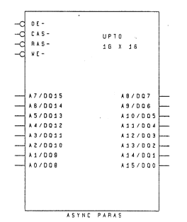
view of an illustrative or exemplary 24-pin asynchronous
4M x 4 baseline asynchronous DRAM and control lines and
pins adapted for the prac~ice of the invention;
Fig. 2 is a similar view of a 44-pin synchronous
~DRAM version;
Figs. 4 and 3 are control line signal and operational
timing diagrams of the method and sequence of operating
the device of Fig. 1 in accordance with the present inven-
tion, showing addressing and data accessing during the
write and read cycles, respectively;
Fig. 5 is a bloc~ and circuit diagram of apparatus
for operating the synchronous device of Fig. 2 in accord-
ance with the technique and interfacing of the invention;
Figs. 7 and 6 correspond, respectively, to the timing
and operation diagrams of Figs. 4 and 3, but are directed
to the operation of the~~DRAM device of Figs. 5 and 2 in
~ 2159953
-14-
accordance with the invention;
Figs. B and 9 are block diagrams respectively showing
4M x 64 and 16M x 64 configurations embodying dynamic
random access memory devices of the invention; and
Fig. 10 is a similar diagram contrasting the prior
art with the system of Fig. 9.
Description of Preferred Embodiment(s)
As before stated, the invention (coined 'PARA~') has
a distinct external circuit interface and a unique access
mechanism which differ radically from the before-described
existing techniques used by either the async DRAM or
~DRAM.
In accordance with the invention, the row address is
provided on a set of pins, followed by column address, and
then data is transferred over the same pins. The data to
be stored during the write cycle follows the column
address, instead of, as in current existing access
mechanism approaches being presented to the DRAM simultan-
eously. While this may have some adverse impact
-15- 21599~3
on the write timing for the single access and on the first
write of the burst access this is deemed trivial as
impaired with the extrordinary advantages of the inven- -
tion. The data retrieval for read access, moreover, is
not substantially affected.
This unique access mechanism of the invention can be
beneficially used in two ways:
1. If it is desired to maintain compatibility with the ex-
isting standard package sizes of the DRAM, then the inven-
tion enables the data bandwidth and addressing capability
within the similar package to be increased dramatically.
With the invention, the number of data bits increases
as data is also tranferred over DRAMs. The addressing
capability of the invention also enhances as the address
is alqo providedover what are currently used as the data-
only pins in the existing factor of four for every data
pin offered in the existing DRAMs. For example, in the
'PARA~' system of the invention, the number of uniquely
addressacle locations will quadruple for a single-bit cur-
rent existing DRAM; will be 256 times more for a 4-bit
wide current DR~M; 65536 times more for an 8-bit wide
. 21S9953
-16-
current existing DRAN; will be 256 times more for a 4-bit
wide current DRAM; 65536 times more for an 8-bit wide
existing DRAM, and so on. The equation is 22n times addi-
tional addressing capability for an'n'bit wide convention-
al DRAM.
This tremendous gain in both address and data band-
width is acheived, moreover, without increasing the number
of pins of the current DRAM.
2. Another option is eo reduce the DRA~ pin count and
stiil get similar data bandwidth and addressing capability
currently provided by the existing DRAM devices, but with
a reduced or smaller package size.
With the novel access mechanism of the invention,
devices can thus be built with smaller packa~e sizes. For
example, a 256K x 16 DRA~ which is currently provided in a
40-pin package can be reduced down to 24 pins and still
provide higher density. This reduction will have major
impact on both the board space, power consumption and
other problems outlined above.
The impact of this proposed access mechanism is fur-
ther illustrated by using an existing 4~ ~ 4 DRAM as an
example, but is, of course not limited to this size DRA~
only.
~ 2I59953
-17-
In this example, twenty two address bits are required
to decode 1 out of 4 Meg storage cell locations. These 22
pins are split as either 11 pins for both row and column
address or 12 pins for row and 10 for column address in
current state of the art DRAMs. With the invention, on
the other hand, where data is sequenced over the same 12
pins used for row/column address, an additional 12 data
bits become available along with 4 original data bits to
the external circuit. This results in the total bandwidth
of 16 data bits and without increasing the package pin
count. Thus, only four 'PARA~" chips of the invention are
required for a 64 bit wide data bus in this context-- a
decided advantage over the traditional approach where a 64
bit wide bus needs 16 chips of similar package size.
Continuing the example of a current 4M x 4 DRAM,
similar to that of the before referred ~amsung catalog, 4
data bits DQ3, DQ2, DQ1 & DQO of such a traditional DRAM
are also used for in Figs. 1 and 2, DRAM illustrative
async and ~DRAM respectively, for row and column addresses
during the address phase. This enables the availability
of 4 additional address lines in the conversions of the
invention, thus effectively resulting in 8 additional
address lines. Using the multiplication factors described
earlier, the number of addressable DRAM memory locations
21~99~3
-18-
can, by the present invention, be increased by 256 times
without increasing the package size. In fact, in this
specific context, the address range ~ill increase by 1024
times due to already assigned 12 address bits, when only
11 are needed.
It should now be pointed out that when implemented by
the invention, a state of the art 24-pin package 4M x 4
async DRAM is capable of accomodating up to 4G x 16 bits
(that is 64 Gigabits) -- an amazingly wide range. In fact
development of 64 Gigabit DRAM had not even been expected
in this century.
~ imilarly, when implemented as sync DRAM ('PA~A~') a
state of art 44-pin package 4M x 4 ~DRAM can also accomod-
ate up to 4G x 16 or 64 Gigabits.
These gains for the 4M x 4 example represent better
than 3 orders of magnitude improvement in storage
capability in a comparable size package over current
existing DRAMs.
In the top level symbolic presentations of async and
sync versions of the invention in Figs. 1 and 2 for the
example described above, the pins and control lines are
~' 21~99S3
not listed for purposes of clarity, stressing just the
novel features of the invention, and with conventional
ground, power and byte select being omitted for better
understanding only.
While in a wide range of instances comparability with
current DRAMs is described it should be noted that;
'PARA~' is not guaranteed to be pin compatible with the
existing devices always, but is expected to stay within
the similar package sizes. This is specifically true for
the sync version where some commands definition using
address bits 'A10' & 'All', Fig. 2, will have to be
changed or defined differently to implement 'PARA~' access
mechanism; though the overall package size remains the
same or nearly the same.
As stated earlier, there is sometimes a possibilty
that DRAM access might be slightly slower with the inven-
tion due to the shared usage of the same set of pins for
different access phases, but the technique has overwhelm-
ing significant improvements. The exact impact on access
time may indeed be negligible or none at all depending on
the implementation. The read access is expected to be as
~ 2159953
-20-
fast and any delay will affect only the write cycles.
Various implementations are possible for this architecture
differing only in features and details, but with the same
essential idea of the invention. The two major types of
implementations, asynchronous mode and synchronous mode,
will now be described in more detail.
Turning first to the asynchronous mode: the access
for such implementation is shown in Figs. 3 and 4 as
correlated with the structure of Fig. 1. A row address is
first provided using 'ras' (row address strobe), Figs. 1,3
and 4, as the control line. Next, the column address is
presented over the same pins under the control of 'cas'
signal.
In the case of the write cycle, "data" is driven or
applied on the same pins after the "column address", as
shown in Fig. 4. Hence the first write access will be
slightly slower (since data appears after the column
address on the same pins); but the subsequent accesses to
the consecutive columns in the same row will be similar to
the existing async DRAMs.
-21- 21 ~995~
In the case of the read cycle, however, Fig. 3,
"data" is retrieved over the same pins, and sequencing of
"row address", "column address" and "data", respectively,
will still have timings similar to the existing async
DRAM. ~ince, in general with both the asynchronous mode
and the later described synchronous, far more numbers of
reads are performed in a typical system than writes, the
before-suggested minor performance degradation during
write cycles will not be significant. In addition, if
cache is used in the system design, this slight degrada-
tion will further diminish to very low levels.
A syncronous ('PARA~') DRAM top level internal block
diagram is shown in Fig. 5 for ease of explanation only.
A clock and clock enable signal is provided in such type
of DRAM and the acce~s for such an implementation is shown
in Figs. 6 and 7 and in the context of the device of Fig.
2. ~ere, the traditional names such as 'ras', 'cas' etc.
take additional meanings as they are also used to load
control commands. The row address- is loaded with a
'ras' pulse and an appropriate combination of other con-
trol signals. Next, the "column address" is loaded over
the same pins with 'cas' being low and with appropriate
-~2- 21S99~3
state of other signals. There are other commands such as
~activation', 'deactivation' 'precharge' etc. It should
be noted that in existing sync DRAM standards some com-
mands can be issued during data phase which use 'A10' and
'All' pins. In the adaption of the invention, these com-
mands are redefined and executed differently, resulting in
usage of two additional pins; but the overall package size
may still be the same.
In the case of the write cycle, 'data" is driven over
the same pins after the "column address", as shown in
Fig. 7. The first write access is expected to be one
clock cycle slower than the traditional synchronous DRAMs,
but the subsequent accesses in the same row will be every
clock cycle. The exact delay for the first write access
is subject to implementation and device technology.
Uith the read cycle, "data is retrieved over the
same pins after the "column address' is presented, as
shown in Fig. 6 and sequencing of row address', column
address" and 'data", respectively, will have timings simi-
lar to existing sync DRAMs, as shown.
-23- 21 ~9g~s3
Continuing with an exemplary system level implementa-
tion using the 'PARA~' technique of the invention, and
assuming the illustrative example of the 4M x 64 memory
array requirement only four 4m x 16 'PARA~' type DRAMs (24
pin package, in the case of async 'PARA~' and 44 for sync
'PARA~') are needed, Fig. 8, to achieve the desired con-
figuration, instead of sixteen current existing access
mechanism based 4M x 4 DRAMs, presuming comparable package
size devices are used. This saves considerable board
space, reduces power consumption, provides better MTBF and
a drop in compatibility with higher density DRAMs for
future expansion.
As greater system memory requirements are required in
the future, from 4M x 64 to 64M x 64, the 64M x 16 'PARA~'
DRAMs can be dropped in place of 4M x 16, as they will be
pin compatible. This contrasts with prevailing technology
where a new board design and subsequent significant manu-
facturing related expenses must be incurred. Time to
market is a major factor and will be seriously affected,
since 4M x 4 existing DRAMs are not pin compatible with
future 64M x 4. As stated earlier, moreover, the inven-
-24- 21 sg9~3
tion is capable of accomodating storage sizes 256 times
larger for x 4 configuration of existing DRAMs and 65536
times for x 8 configuration of existing DRAMs with the
comparable package size.
And though there are presently existing devices of
witer data bandwidth, they also have much larger pac~age
sizes as contrasted further with the invention.
As frequently pointet out, the invention also pro-
vides much finer granularity than the existing sync or
async DRAMs and consumes far lower numbers of components
when multiple banks are used in the design. If, as an
example, 4 separate banks of 4m x 64 are needed, Fig. 9,
the based array of the invention would need only 16
devices, as shown. This compares well against the
exi~ting async or aync DRAM-based implementation, which
will consume 64 components, as shown in Fig. lO.
A column address counter, furthermore, is preferably
incorporated in the invention to facilitate sequential
access fast-page mode and with faster access than the
traditional async design; the invention, in all cases,
providing increased address and data bandwidth and, where
desired, resulting in substantially lower numbers of
' -25- 21 S99~
components. The system and technique of the invention are
thus expected to be immensely useful for large numbers of
applications and serving as a critical component for
designs where space and power consumption are at a
premium.
In the external circuit interface, the memory con-
troller has different sequencing and timings, as before
explained, than what traditional DRAM designers employ,
with the multiplexer circuit used to multiplex the row and
column address being of tristate type, Fig. 3, 4, 6 and 7,
to allow for the data to reside on the same bus.
In conclusory summary, with the use of the inven.ion,
the package size is kept comparable with current devices,
but the number of data bits has increased significantly.
The increased data bandwidth at each part results in
significantly reduced number of parts required to meet the
wider data bus size, and the package size is kept the same
or nearly the same, but with the number of uniquely
addressable locations increased significantly.
A most significant advantage of 'PARA~' resides in
the larger data bandwidth and higher potential density
~, 21S9953
-26-
which have a significant impact on the system implementa-
tion, enabling reduced board "real estate", lower power
consumption, reduced manufacturing cost, and a large range
of drop-in pin compatibility.
Further modifications will occur to those skilled in
this art, and such are considered to fall within the
spirit and scope of the invention as defined in the appen-
ded claims.