Note: Descriptions are shown in the official language in which they were submitted.
216Q28~'
._ . -- 1 --
HIGH EFFICIEN~Y MICROSTRIP ~.l~N~AS
Related Applications
This application is related to our co-pending
applications entitled "IMPROVEMENTS IN SMALL ANTENNAS SUCH
AS MICROSTRIP PATCH ANTENNAS" (Evans 19-25-9) and "ANTENNAS
WITH MEANS FOR BLOCKING CURRENTS IN GROUND PLANES" (Evans
20-26-10), both filed concurrently herewith and assigned to
the same assignee as this application.
Field of the Invention
This invention relates to microstrip antennas, and
particularly to high efficiency microstrip antennas.
Back~round of the Invention
Microstrip antennas and their histories are
described in the "Proceedings of the IEEE", Volume 80, No.
1, January 1992. The basic configuration of the microstrip
antenna is a metallic conductor, such as a patch printed on
a thin, grounded, dielectric substrate. This element can be
fed either with a coaxial line through the bottom of the
substrate or by a co-planar microstrip line. A microstrip
antenna radiates a relatively broad beam broadside to the
plane of the substrate.
Because of the skin effect, currents in a
microstrip antenna flow mainly in the outer and inner
surfaces of the conductor, for example the patch. The inner
surface of the patch adjacent the dielectric substrate,
faces the ground plane. Accordingly, the current on the
inner surface is substantially higher than the current on
the outer surface. However, it is mainly the outer surface
which radiates or receives radiation. Currents on the inner
surface are incapable of producing radiation because the
conductive portion of the patch between the outer and inner
surface blocks radiation which the current at the inner
surface may generate. This limits the efficiency of the
radiation.
An object of the invention is to improve
microstrip antennas.
Summary of the Invention
According to an aspect of the invention, a microstrip
antenna includes a ground plane, a dielectric substrate over
the ground plane, and having, deposited on the dielectric, a
microstrip conductor, such as a microstrip patch. The
microstrip patch has a thickness sufficiently small to make
the conductor substantially transparent to radiation at the
frequency at which the antenna is to operate. In one
embodiment, the conductor has a thickness from 0.5~ to 4
where ~ is the skin depth at the antenna operating frequency,
and preferably ~ to 2~.
According to an aspect of the invention, the conductor
is in the form of a patch.
In accordance with one aspect of the present
invention there is provided a microstrip antenna for operation
at a predetermined frequency, comprising: a ground plane; a
dielectric substrate on said ground plane; and a microstrip
conductor arrangement having a microstrip conductor deposited
on said substrate; said microstrip conductor having a
thickness sufficiently small to be substantially transparent
to radiation at the predetermined frequency, where transparent
is defined as permitting RF currents on an inner surface of
said microstrip conductor to produce radiation, said inner
surface being adjacent and facing said ground plane.
These and other aspects of the invention are pointed
out in the claims. Other objects and advantages of the
invention will become evident from the following detailed
description when read in light of the accompanying drawings.
Brief Description of the Drawinqs
Fig. 1 is a perspective view of a microstrip antenna
embodying features of the invention.
Fig. 2 is a cross-sectional view of the microstrip
antenna in Fig. 1.
Fig. 3 is a cross-sectional view of another antenna
embodying features of the invention.
1~
-
- 2a -
Fig. 4 is a plan view of the microstrip antenna in
Fig. 3.
Fig. 5 is an end elevational view of the microstrip
antenna in Fig. 3.
Fig. 6 is a perspective view of another antenna
embodying features of the invention.
Detailed Description of Preferred Embodiments
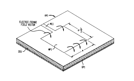
Figs. 1 and 2 illustrate perspective and cross-
sectional views of a microstrip antenna AN1 embodying
, ~ s
. . ~ ~.
- 21602~
- 3 -
features of the invention, with thicknesses exaggerated for
clarity. In Fig. 1, the microstrip antenna AN1 includes a
microstrip line ML1 which feeds a microstrip patch MP1
deposited on a dielectric substrate DS1, and a ground plane
GP1 under the dielectric substrate.
According to an embodiment of the invention, the
thickness of the microstrip patch MP1, namely its distance
from its upper surface US1 to the inside surface IS1
adjacent the substrate DS1 is sufficiently small so that the
patch becomes substantially transparent to radiation over
the range of frequencies at which the antenna AN1 operates.
This allows the larger current i2 at the inner surface IN1
of the patch MP1 facing the dielectric substrate DS1, and
hence facing the ground plane GPl, to couple with, and add
its effect on radiation, to the smaller current i1 at the
upper surface USl. A current i3 flows in the ground plane
and is substantially equal to i1 + i2. Hence, the invention
overcomes the undesirable effect of conductive material
between the upper and the inside surfaces of prior
microstrip antennas shielding the radiation produced or
sensed by the currents in the inner surface.
The antenna AN1 in Fig. 1 is linearly polarized.
The length of the patch in Fig. 1 is, for example A/2, where
A is the wavelength of the center frequency of the operating
range of the antenna AN1.
According to an embodiment of the invention, the
thickness of the microstrip patch MP1, namely the distance
between its upper surface US1 and the inside surface IS1
adjacent the dielectric substrate DS1 is equal to 0.5 ~ to
4~ and preferably ~ to 2~, where ~ is the skin depth. The
skin depth depends upon the frequencies at which the antenna
AN1 is to operate. The operating frequency is, for
practical purposes, the center frequency of the range of
frequencies at which the antenna is to be used. Skin depth
is defined in the book "Reference Data For Engineers:
216028~
- 4 -
Radio, Electronics, Computer, and Communications", seventh
edition published by Howard W. Samms and Company, A Division
of MacMillan, Inc. 4300 West 62nd Street, Indianapolis,
Indiana 46268. The skin depth ~ is that distance below the
surface of a conductor where the current density has
diminished to 1/e of its value at the surface. At 2.5
gigahertz (GHz), the skin depth in copper is about 1.5
micrometers (~m). Thus in one embodiment the thickness is
0.75~m to 6~m and in another 1.5~m to 3~m in copper.
In operation, a transmitter and receiver are
connected across the stripline MS1 and the ground plane GP1.
In the transmit mode, the transmitter applies voltage across
the microwave stripline ML1 and the ground plane GP1 at a
microwave frequency such as two GHz. The currents appearing
at the upper and inner surfaces US1 and IS1 of the microwave
patch MP1 couple to each other and add to produce radiation
transverse to the plane. The microstrip antenna MA1 then
radiates a relatively broad beam broadside to the plane of
the substrate. In the transmit mode, the invention
increases the radiation output because the transparency of
the microstrip patch MP1 according to the invention permits
the surface currents i1 and i2 to couple and effectively
allows radiation from the inner surface IS1 through the
transparent patch.
In the receive mode, the microstrip antenna MA1
and the path of propagation of radiation at frequencies such
as two GHz. The latter generate currents in both the upper
and lower surfaces US1 and IS1 of the microstrip patch MP1.
More specifically, the currents in the upper and lower
surfaces couple to each other and operate in additive
fashion. The microstrip line ML1 and the ground plane GP1
pass the currents to the receiver in the receive mode. The
currents passed to the receiver are therefore substantially
higher than would be available from microstrip patches
thicker than those of the present invention, because the
21 60284
- 5
patches would not be transparent to radiation. The lack of
transparency would effectively prevent significant current
in the inner surface IS1, and allow the receiver to sense
currents only in the upper surface US1.
Fig. 3 illustrates another embodiment of the
invention which takes advantage of the transparent
characteristics of the patch MP1 in Fig. 1. Here,
dielectric spacer layers SL31 and SL32 space three
microstrip patches MP31, MP32, and MP33 deposited on a
dielectric substrate DS31 over a ground plane GP3. Fig. 4
is a plan view, and Fig. 5 a side elevation, of the
microstrip antenna in Figs. 3. In Figs. 3, 4 and 5 the
thicknesses are also exaggerated for clarity. Metal walls
MW31 and MW32 are deposited on each side of the dielectric
spacer layers SL31 and SL32 and the three microstrip patches
MP31, MP32, and MP33 to connect the three microstrip patches
so they are at the same potential. Suitable microstrip
lines ML31, ML32, and ML33 connect the microstrip patches
MP31, MP32, and MP33 to the edge of the dielectric substrate
DS3 for connection to the output of a transmitter and the
input of a receiver. The dielectric spacer layers SL31 and
SL32 also space the lines ML31, ML32, and ML33. The sides
of the lines ML31, ML32, and ML33, as well as the spacer
layers SL31 and SL32 are covered by metal walls MW33 and
MW34. The walls are not intended to have load bearing
capability but only to provide conductive connections
between the metal layers and lines to maintain them at the
same potential. According to another embodiment, one or
more of the metal walls are omitted.
In the transmit mode, currents appearing in the
upper and inner surfaces US31 and IS31, of each of the
patches add with each other to produce enhanced radiation.
Here the radiation arising from currents in the upper and
inner surfaces US33 and IS33 of the microstrip patch MP33
add to the radiation produced by currents in the upper and
21S0284
inner surfaces US32 and IS32 the patch MP32, and currents in
the upper and inner surfaces US31 and IS31 of the patch MP31
because of the transparent nature of each of these patches,
each of which has a thickness equal to 0.5 ~ to 4~ and
preferably ~ to 2~. At 2.5 GHz the skin depth ~ is about
1.5 ~m.
The currents in the three microstrip patches MP31,
MP32, and MP33 tend to hug the edges. The purpose of the
metal walls MW31, MW32, MW33, and MW34 is to place the edges
of the three microstrip patches MP31, MP32, and MP33 and
lines ML31, ML32, and ML33 at the same potential.
According to another embodiment of the invention,
the dielectric spacer layers SL31 and SL32 extend beyond the
edges of the microstrip patches MP31, MP32, and MP33, and
preferably to the edges of the dielectric substrate DS31.
According to other embodiments of the invention,
variations in patch shape along the width and length,
feeding techniques and substrate configurations, and array
geometries are employed. Such variations correspond to
known variations, but incorporate the patch thickness
disclosed. An example appears in Fig. 6 showing an antenna
AN6 with an eight patch array.
The transparency of the conductors allows an
increase in the efficiency and bandwidth of the operation of
the antenna.
While embodiments of the invention have been
described in detail it will be evident to those skilled in
the art that the invention may be embodied otherwise without
departing from its spirit and scope.