Note: Descriptions are shown in the official language in which they were submitted.
IMPROVEMENTS IN SMALL ANTENNAS
SUCH AS MICROSTRIP PATCH ANTENNAS
Field of the Invention
This invention relates to micro-dimensioned
electromagnetic radiators, and particularly to microstrip patch
and other small antennas.
Background of the Invention
A small antenna is defined as a conducting radiator
with overall dimensions of less than Ao/2, where Ao is the
wavelength of the propagating signal in free space. The
properties of a class dipole antenna with a length of A/2 are
described in detail in the book by John D. Kraus, "Antennas",
McGraw Hill 1988.
Efforts to shrink the length of the resonating dipole
antennas have resulted in small antennas known as microstrip
antennas constructed of dipoles or patches deposited on
dielectric substrates. Microstrip antennas are described in the
Proceedings of the IEEE, Vol. 80, No. 1, January 1992 in the
article entitled "Microstrip Antennas" by David M. Pozar.
An object of the invention is to improve small
antennas.
Summary of the Invention
According to an aspect of the invention, an antenna
includes a resonating conductive arrangement having an overall
dimension L, a first dielectric contacting the conductive
arrangement along the dimension L and having a dielectric
constant ~ r11 and a second dielectric covering the first
dielectric and having a dielectric constant with a value ~ r2
between the value ~ r1 and an ambient dielectric constant.
In accordance with one aspect of the present invention
there is provided an antenna, comprising: a ground plane; a first
dielectric contacting and covering substantially all of a surface
of said ground plane and having a substantially continuous
thickness and having a substantially uniform dielectric constant
~ '
~ ~1 6~ 28 ~
-- 2
~rl i a conductive patch having a length L and contacting said
first dielectric so as to sandwich at least a portion of said
first dielectric between said patch and said ground plane, said
patch forming a radiating element; a second dielectric
sandwiching the first dielectric and the patch between the second
dielectric and the ground plane, and having a dielectric constant
with a value ~r2 representing a geometric mean value between the
value ~r1 and an ambient dielectric constant of an ambient
dielectric propagating medium; said radiating element being the
only radiating element in a range from the ground plane with the
surface all covered by the substantially continuously thick first
dielectric with the uniform dielectric constant, to the ambient
dielectric propagating medium, and through the second dielectric
sandwiching the first dielectric and the patch and having a
dielectric constant with a value ~ r2 representing a geometric
mean value between the value ~r1 of the first dielectric and the
ambient dielectric constant of the ambient dielectric propagating
medlum .
In accordance with another aspect of the present
invention there is provided the method of forming a patch
antenna, comprising: placing a first dielectric having a
substantially uniform dielectric constant ~r1 and a substantially
continuous thickness on a ground plane; supporting a microstrip
patch having a length L with the first dielectric so as to form
a microstrip patch antenna section with said first dielectric and
said ground plane; and covering the first dielectric, having the
substantially continuous thickness and substantially uniform
dielectric constant, with a second dielectric having a dielectric
Constant ~r2 = ~ + 30~, and a thickness d = L/(2 ~ ) + 30~,
and ~ ~ 1, so as to sandwich the first dielectric between said
second dielectric and said first dielectric, and so as to match
the dielectric constant of the first dielectric with the
dielectric constant of 1 by means of a dielectric constant which
':
- 2a -
is a substantial geometric mean of the first dielectric constant
and 1, while maintaining the patch as the only patch on the
antenna.
These and other aspects of the invention are pointed
out in the claims. Other objects and advantages will become
evident from the following detailed description when read in
light of the accompanying drawings.
Brief Description of the Drawings
Figure 1 is a sectional view of an antenna embodying
aspects of the invention.
Figure 2 is a cross-sectional view of a microstrip
patch antenna embodying aspects of the invention.
Figure 3 is a plan view of the antenna in Figure 2.
Figure 4 is a cross-sectional view of another
microstrip antenna embodying aspects of the invention.
Figure 5 is a cross-sectional view of another
microstrip antenna embodying aspects of the invention.
Figure 6 is a cross-sectional view of another
microstrip antenna embodying aspects of the invention.
Detailed Description of Preferred Embodiments
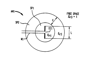
Figure 1 illustrates an antennal ANl embodying the
invention and using the fundamental dipole antenna structure.
The arrangement permits shrinking of the physical conductor
dimensions of a classic dipole antenna with a length of ~/2
without substantially altering the antenna characteristics, and
increasing its efficiency.
In order to shrink the length of the resonating
dipole by a factor S (shrinking factor), a dipole DIl
connected to lead wires WIl is embedded in a small sphere
SPl composed of core dielectric material. This spherical
volume is termed the "the near field sphere". The relative
dielectric constant of the material in the near field sphere
SPl is ~ r1 ~ The central sphere SPl is surrounded by a
spherical shell SP2 with a relative dielectric constant
CA 02160286 1998-10-29
- 3
erz = ~ . The shell SP2 is embedded in free space with a
relative dielectric constant ~r3 = 1. The shell SP2 with
dielectric ~r2 iS termed the "matching shell~ or l'matching
layer." The matching layer SP2 matche~ a low impedance to
a high impedance load or vice versa. The lead wires Wl
serve for connection to a receiver or transmitter (not
shown). The relative dielectric constant erl of the core
dielectric material of sphere SP1 results in a shrinking
factor S = ~ .
The length L of the resonating Half-wavelength
dipole DI1 is L = 2 = 2~ with a corresponding shrinking
factor S = ~ . The value Ao is the center wavelength of
the resonating antenna in free space.
The thickness d of the matching shell SP2 is a
quarter-wavelength within the dielectric medium SP2 with the
relative dielectric constant of ~r2~ namely A/4 or
lo/(4 ~/~ ). This matching dielectric constant er2 iS the
geometric mean between ~rl and er3r and is given by Er2
= ~e~ler3 ~ ~ where er3 = 1.0 in free space and close to
1.0 in ambient air with the result d = Ao/ ~
lo/~4 4 ~ ).
Thus for example: If the frequency fO = lGHz and
- 4 2160Z8&
., .,.,~ ,
Crl =38, Ao = 0.33, m = 12 ", Cr2 =
and d = lo/(4 )=1.2". In this case L= 12/(2 x 6.2) =
0.97~
The matching shell SP2 reduces the effects of
substantial reflections and other disadvantages arising from
the dielectric mismatch between the shell SPl and free
space. Preferably, the thickness d of the matching shell
SP2 is one quarter wavelength of A or Ao/(4 ~ ) so the
incoming waves are 180~ out of phase with the reflections
that occur at the boundary of the matching shell and free
space, and therefore cancel reflections from that boundary.
In effect the matching layer introduces a gradual change in
dielectric constant from sphere SP1 to sphere SP3 and that
limits reflections. This has the effect of broadening the
bandwidth propagated.
The dielectric constant cr2 of the matching layer
SP2 is chosen as the geometric means between c rl and c r3 ~
namely Cr2 = ~CriCr3 = ~, because this spreads the change
in dielectric constant uniformly among the boundaries SP1-
SP2 and SP1-SP3.
According to an embodiment of the invention,
additional quarter wavelength dielectric spheres or layers
cover the--sphere SP2.
The dielectric constants of these added layers decrease from
the dielectric constant crl of the sphere SP1 to the
dielectric constant of the sphere SP3, namely cr3=1. This
provides gradual changes in dielectric constants.
Preferably, the dielectric constant of each of all n
overlying matching layers, including the sphere SP2, is then
- S - 2160~8~
the next lower (n+1)/p-th root of ~rl where ~r3 = 1 . This
spreads the change in dielectric constant uniformly among
the boundaries between spheres SP1 and SP3. Increasing the
number of matching layers improves the efficiency even
further and broadens the bandwidth.
The addition of the matching layer SP2 favorably
affects the radiation resistance Rr of the antenna AN1. As
shown in the aforementioned book "Antennas" by John D. Kress
, the radiation resistance of a dipole antenna is 73 ohms.
With a single matching layer SP2 as shown in Figure 1, the
radiation resistance Rr of the antenna AN1
reduced by a factor ~ from the resistance of 73 Ohms.
Hence, in addition, to shrinking the physical size of the
radiation system, the invention achieves a reduction of the
radiation resistance to Rr = 73/ ~ -
The radius of the near-field-sphere SP1
satisfies the condition 1/(2~) 2 ~ r/A ~ (2~). This will
cover the volume where the stored electromagnetic reactive
energy is dominant and exceeds the radiated energy per
signal cycle.
Figures 2 and 3 are cross-sectional and plan views
of a microstrip patch antenna PA1 embodying the invention
and applying the aforementioned matching of a radiating
structure to free space. Here, a conductive ground plane
GP1 supports a near field dielectric substrate layer DL1
which embeds a patch resonator PR1. A matching dielectric
layer DL2 overlies the layer DL1.
The conductive patch resonator PRl is rectangular
in shape with a length L=Ao/(2 ~ ) and a width w. A
conductor COl connects the patch resonator PR1 to the edge
of the antenna PA1 for connection, with a connection to the
CA 02160286 1998-10-29
- 6
ground plane GP1, to a receiver or transmitter (not shown).
The near field substrate layer DL1 serves the same purpose
of the sphere SPl and has a relative dielectric constant ~rl.
To embed the patch resonator PR1, the near field substrate
layer DLl is thicker than the spacing of the patch resonator
PRl to the ground plane GPl. The distance d2 between the
patch resonator PR1 and the matching dielectric layer DL2 is
preferably L/2~. This approximates the radius of the sphere
SPl if the dipole DI1 is nearly equal to the radius of the
sphere SP1.
The matching dielectric layer DL2, serves the same
purpose as the matching layer SP2
of Figure 1 and has a relative dielectric constant l!:r2 =
~-
The thickness of the quarter-wave matching layer
is given by d= ~ =AJ (44 ~ )
According to another embodiment of the invention,
additional matching quarter wavelength (in thickness) layers
are placed over the matching dielectric layer DL2. In such
cases, as in the case of the sphere, n matching layers each
have dielectric constants that decrease sequentially from erl
to 1 in the layers starting with the layer DL2. Preferably
the layers have dielectric constants of the next lower of
the (n+l)/p-~h root of e~l, where p z n, ...2, 1 for each
layer further from the substrate This spreads the change
in dielectric constant uniformly among the boundaries
between the layer DL1 and free space. It spreads the
changes of dielectric constants at the boundaries, and
causes cancellation of reflections within each quarter
wavelength layer because of the 180~ phase displacement
between wave and reflection. ~t increases efficiency and
CA 02160286 1998-10-29
- 7 -
other characteristics such as bandwidth.
Another embodiment of the invention appears in the
cross-sectional view of an antenna PA2 in Figure 4. In this
embodiment the plan view (not shown) is the same as in
Figure 3. Here, the near-field substrate layer is
designated DL4 instead of DLl as in Figure 3. The cross-
sectional view of Figure 4 differs from Figure 2 only in
that in Figure 4 the thickness of the near-field substrate
layer DL4 is equal to the height of the patch resonator PR1
above the ground plane GPl. The relative dielectric
constants are the same as in Figures 2 and 3. The thickness
of the quarter wave matching layer DL2 is also the same as
in Figure 2.
Figure 5 is a cross-sectional view of an antenna
using a patch generator as shown in Figures 2 and 3 but with
a quarter wavelength matching layer DL12 and additional
quarter wavelength matching layers DL13 and DL14. The layer
DL1 is qplit into two dielectric layers having the same
dielectric constant and receive the patch resonator PR1
between them. The dielectric constants decrease ~rl at the
layer DLl toward 1. Here, the dielectric constants of the
layers DL12, DL13, and DL14 are ~ , ~ , ~
Figure 6 i~ a cross-sectional view of an antenna
using a patch generator as shown in Figure 4 but with a
quarter wavelength matching layer DL22 and additional
quarter wavelength matching layers DL23, DL24, and DL25.
Here, the dielectric constants of the layers DL22, DL23,
DL24, and DL25 are erl4/5~ ~ 13/5 e 2/5 and ~ 1/5
In operation, the antenna AN1, PA1, and PA2
connect via wire lines W1 and conductors C01 to respective
receivers or transmitters (not shown). In the receive mode,
for the length L, they respond to frequency ranges centered
2160285
-- 8
,.~
on the frequency fO having a wavelength Ao =2L ~ , (fO
=Co/(2L ~ ) where C0 = velocity of light in free space.
In the transmit mode, they radiate over frequency
rangers centered on the same frequency. The matching
dielectric layers prevent the waves, as they propagate
through one medium of one dielectric constant, from
encountering a medium with a vastly different dielectric
constant. Each such encounter results in reflections that
limit the efficiency and other characteristics of the
0 radiation, such as the bandwidth. The matching layers
interpose one or more media of intermediate dielectric
constant, with each dielectric constant being the geometric
mean between the dielectric constant of adjacent layers,
such as ~ , where n is the number of matching layers,
p is the sequential number of any matching layer ending with
the layer next to the substrate, and ~rl is the dielectric
constant of the substrate layer. Because the thickness of
each matching layer i8 one quarter wavelength of the
matching layer medium, or Ao/(4~r1) if the layers are equal,
the waves entering the matching layer are 180~ out of phase
with waves reflected in the medium and hence cancel the
reflection.
Because Ao = 2L ~ ~ fo=Co/(2L ~ ), the
thickness of the matching layers may be chosen by the
preferred relationship d = L/(2 ~ ). According to an
embodiment of the invention this relation may vary over a
tolerance of + 30~.
In making antennas, such as the patch antennas PA1
216G ~8 ~
and PA2, the length L and the dielectrics DLl and DL2 are
chosen depending on the desired center frequency preferably
on the basis of (equation). According to an embodiment of
the invention, the relationship may vary over a range of +
5 30~ because of the bandwidth of the resonator. The
dielectrics SP2, DL2, and DL4 and the distance d are chosen
on the basis of the dielectrics SPl and DLl as well as the
center frequency fO by way of a preferred relationship such
as lo/(4 ~ ). According to an embodiment of the invention
this relationship may vary over a tolerance of 30%.
Because Ao = 2L ~ ~ fo=Co/(2L ~ ) the thickness
of the matching layers may be chosen by a preferred
relationship d=L/(2 ~ ). According to an embodiment of
the invention this relationship may vary over a tolerance of
30%.
The values of the dielectric constants and
thicknesses need not be exact but may vary. Within the
matching layers, any dielectric constant between the
dielectric constant of the substrate and free space improves
the operation as long as they approach the dielectric
constant of free space the closer they are to the free space
in the antenna.
The invention results in a smaller antenna that
retains the efficiency of a larger antennas, or put
otherwise, produces antennas of greater efficiency other
than antennas of equal size.
The invention also prevents a collapse of the
bandwidth observed for conventional antennaq if their size
is substantially reduced from Ao/2.
An embodiment of the invention incorporates the
disclosure of our aforementioned concurrently-filed
21~028~
,- 10 -
copending application entitled "High Efficiency Microstrip
Antennas" by making the thickness of the conductor
sufficiently small to reduce shielding and losses caused by
the skin effect and make currents at the upper and lower
surfaces couple with each other and make the conductor
partially transparent to radiation. In one embodiment the
thickness is between 0.5~ and 4~. Preferably the thickness
is between 1~ and 2~ where ~ is equal to the distance at
which current is reduced by l/e., for example 1.5 to 3
micrometers at 2.5 gigahertz in copper. According to an
embodiment, alternate layers of dielectrics and radiation
transparent patches on a substrate enhance antenna
operation.
An embodiment of the invention incorporates the
disclosure of our aforementioned concurrently-filed
copending application entitled
"Antennas With Means For Blocking Currents In Ground Planes"
by making dielectric components extend between top and
bottom surfaces of a ground plane in a resonant microstrip
patch antenna over a distance of one-quarter-wavelength of
a resonant frequency of the antenna. The components form
quarter-wave chokes within which waves cancel with reflected
waves and reduce currents in the bottom surfaces of the
ground plane. This reduces back lobe responses.
The content of our co-pending applications
entitled "High Efficiency Antennas" and "Antennas with Means
for Blocking Currents in Ground Planes" both filed
concurrently herewith, and assigned to the same assignee as
this application, are hereby made a part of this application
as if fully recited herein.
While embodiments of the invention have been
described in detail, it will be evident to those skilled in
the art that the invention may be embodied otherwise without
departing from its spirit and scope.