Note: Descriptions are shown in the official language in which they were submitted.
216039~
METHOD OF MAKING AN ORGANIC THIN FILM TRANSISTOR,
AND ARTICLE MADE BY THE METHOD
Field of ~e Invention
This invention pertains to thin film tr~nsictors ( I E;Ts) that comprise an
5 organic active layer, and to methods of making such tr~n.sistors.
Back~l~..l of the Invention
Thin film transistors (TFTs) are known, and are of considerable
commercial significance. For in.~t~nce, amorphous silicon-based TFTs are used in a
large fraction of active matrix liquid crystal displays.
TFTs with an organic active layer are also known. See, for in~t~n(~e, F.
Garnier et al., Science, Vol. 265, pp. 1684-1686; H. Koezuka et al., Applied Physics
~ttPr.~, Vol. 62 (15), pp. 1794-1796; H. Fuchigami et al., Applied Physics Letters,
Vol. 63 (10), pp. 1372-1374; G. Horowitz et al., J. Applied Physics, Vol. 70 (1), pp.
469-475, and G. Horowitz et al., Synthetic Metals, Vol. 41-43, pp. 1127- 1130.
15 These devices typically are field effect transistors (FETs). Such devices potentially
have .~ignifi~nt advantages over conventional TFTs, including a potentially simpler
(and consequently chPapP,-) fabricadon process, the possibility for low temperature
proce~sing, and compatibility with non-glass (e.g, plastic) substrates. Bipolar
tr~n~i~tors that utilize both p-type and n-type organic m~teri~l are also known. See,
20 for in~t~nre, US patent 5,315,129. S. Miyauchi et al., Synthedc Metals, 41-43(1991), pp. 1155-1158, disclose a junction FET that comprises a layer of p-type
polythiophene on n-type silicon.
However, despite considerable research and development effort,
"organic" TFTs have not yet reached commerci~li7~tion~ at least in part due to the
25 relatively poor device characte-i~tic~ of prior art organic 'l'~-l'S.
An important device characteristic of a switching transistor is the on/off
ratio of the source/drain current. Prior art organic l~ ls typically have relatively low
on/off ratios. For in~t~nce, H. Fuchigami et al. (op. cit.) recently reported a device
that had carrier mobility comparable to amorphous silicon, but had an on/off ratio of
30 only about 20. That paper also discloses purification of semiconducting m~teri~l
(PI V) to reduce the carrier scattering by impurities. The m~teri~l had a conductivity
in the range 10-5 - 10-6 S/cm.
H. Koezuka et al. (op. cit.) report fltt~inment of an on/off ratio
(modul~tion ratio) of the channel current of about 105 in a device with doped
35 polypyrole (a highly conducting polymer)-coated source and drain contacts.
According to these fluthors, this is the highest on/off ratio achieved in organic FETs.
21~039~
Nevertheless, the reported on/off ratio is still substantially smaller than on/off ratios
typicaUy available in conventional FETs and demanded for many potential
applications of organic l~ ls. Furthermore, the organic l~ l had very low carrier
mobility (2 x 10~4cm2/V s), and thus would not have been suitable for high-speed5 operation.
In view of the potential significance of organic TE~ l s, it would be
desirable to have available such devices that have improved charactericti~s,
including improved on/off ratio of the source/drain current. This application
discloses such devices, and a method of making the devices.
10 Definitions and Glossary
An "organic semiconductor" herein is a m~teri~l that contains a
substantial amount of carbon in combination with other element,s, or that compri.~es
an allotrope of elemPnt~l carbon (excluding diamond), and exhibits charge carrier
mobility of at least 10-3 cm2 /V s at room temperature (20C). Organic
15 semiconductors of interest for l~ l s typically have conductivity less than about
lS/cm at 20C.
A "p-type" ("n-type") organic semiconductor herein is an organic
semiconductor in which the Fermi energy is closer to (farther from) the energy of the
highest occupied orbital of the molecules or aggregates present in the m~teri~l than it
20 is to (from) the energy of the lowest unoccupied orbital. The term is also int~nded to
mean an organic semiconductor which transports positive charge carriers more (less)
efficiently than negative c~rners. Positive (negative) carriers are generaUy referred
to as "holes" ("electrons").
S~ of the Invenffon
In a broad aspect the invention is embodied in an article that compri~es a
novel organic l ~ l that can have subst~n~i~lly improved characteristics (e.g., on/off
ratio), as compared to prior art organic 'l'~'l'S. A method of making the article is also
disclosed.
Speçific~lly, the organic l~ l compri~es an organic m~ri~l layer,
30 spaced apart first and second contact means (e.g., gold electrodes) in contact with
said layer, and third contact means that are spaced from each of the first and second
contact means and that are adapted for controUing, by means of a voltage applied to
the third contact means, a current between the first and the second contact means
through said layer. Significantly, the organic m~teri~l of the layer is selected from
35 the group consi~ting of -quaterthienylene (a-4T), a-hexathienylene (a-6T), a-
octathienylene (a-~T), a-pent~thienylene (a-5T), a-heptathienylene (a-7T), and a-
3 216039~
nonathienylene (a-9T), each with or without sukstituçnt~ on the 4 or 5 carbon of the
terminal rings (these compounds will collectively be referred to as "a-nT", with n
being an integer from 4 to 9), said organic m~teri~l layer having an electrical
conductivityofatmostS x 10-8 S/cm(preferablylessthanl x 10-8 S/cm)at
5 20C, either in the as-deposited condition or subsequent to a rapid thermal anneal.
In cu~ ly preferred embo~imçnts the organic layer m~tçri~l is a-6T or a-8T, witha-6T being most preferred.
We have made the surprising discovery that, for example, a-6T can be
produced and deposited in a manner that results in a layer of extremely low
10 conductivity, and that a TFT that compri.~es such a low-conductivity active layer can
have greatly improved propellies, including a substantially improved source/drain
current on/off ratio. Indeed, TFTs that comprise the novel active layer m~teri~l can
have an on/off ratio that is comparable to those of the novel (2-layer) TFTs described
in the concurrently filed co-assigned patent application by the same inventors of title
15 "Article Compri~ing an Organic Thin Film Trancistor". Thus, TFTs according to the
instant invention will typically, but not nçcess~rily, comprise a single organic layer,
the "active" layer (but not excluding the presence of, e.g., a protective layer over said
active layer).
In a further aspect the invention is embodied in a method of making a
20 1~-1 that compri~es an a-mT (m = 4, 6 or 8) active layer. The method compri.ses
providing a quantity of a-mT, and depositing a layer of the a-mT on a substrate.The a-mT is produced by a process that compri~es providing a-(ml2) thienyl, de-
protonated in the 5-position, in an organic solvent. Signific~ntly~ the process of
producing said a-mT still further comprises contacting said a-(m/2) thienyl in the
25 organic solvent with a non-halogçn~ting oxidizing agent such that an a-mT-
cont~ining mi~ture is formed, and isolating said a-mT from the mixture. As will be
desc~ibed later in detail, the "isolating" step comprises a multiplicity of substeps.
Although the ~i~cussion below will be primarily in terms of a-6T, we
currently believe that many if not all of the other members of the above defined30 group a-nT can also be synthçsi7~d/treated to meet the specified conductivityrequirement. A prior art method of making compounds such as oc-6T is disclosed in
Chemical Abstracts, Vol. 114, p. 22, item 186387g (1991).
As will be di~cus~d in detail below, a-6T according to the invention
differs from prior art a-6T not only with regard to carrier conce--L,alion but typically
35 also with regard to such characterizing p~pellies as m~l~in~ point, X-ray diffraction
pattern and elçm~nt~l analysis. Similar differences are expected for a-4T and a-8T,
216039~
and indeed for all a-nT. These differences support the conclusion that the active
layer materials according to the invention are essentially new m~teri~l~ that differ
qualitatively from the analogous prior art materials. However, we will refer to
materials according to the invention by the chemical names that have commonly
5 been used to refer to the analogous prior art materials.
Exemplarily, a l ~-l according to the invention, with a-6T active layer,
has exhibited in the as-deposited condition an on/off ratio of more than 106 at 20C,
sukst~nti~lly higher (e.g., by a factor of 102) than the ratios typically exhibited by
prior art organic TFTs. The active layer of the exemplary l ~-l according to the10 invention was only lightly p-type at 20C.
Brief Des~ ,lion of ~he D~.in~s
FIG. 1 schem~ti~lly shows an exemplary prior art ~
FIGs. 2 and 3 schem~tically depict exemplary TFTs according to the
invention;
FIGs. 4 and 5 show data on drain current vs. drain voltage for 2 TFTs
according to the invendon, of somewhat different conductdvides;
FIGs. 6 and 7 show the X-ray diffractdon pattern of, respecdvely, a-6T
according to the invention, and an exemplary prior art a-6T;
FIG. 8 shows exemplary differential scanning calorimetry data for a-6T
20 according to the invention; and
FIG. 9 shows an exemplary drive circuit in an active matrix liquid
crystal display that comprises TFTs according to the invention.
Detailed Descrip~on
FIG. 1 sçhem~tiç~lly depicts a prior art organic TFT 10 of the metal-
25 insul~tor-semiconductor field effect transistor (MIS-FET) type, wherein numerals
11-16 refer, lt;spe~;lively, to substrate, first electrode (e.g., source electrode), second
electrode (e.g., drain electrode), third electrode (gate electrode), in.~ul~tor layer, and
acdve layer.
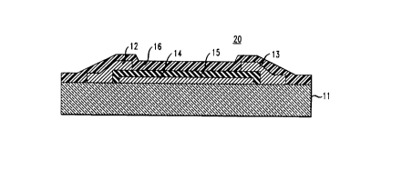
FIG. 2 sc~m~t~ ly shows a MIS-FET type device according to the
30 - inventdon. The tr~nci~tor 20 also compri.~es substrate 11 (e.g., a glass, silicon or
plasdc body), first and second contacts 12 and 13, third contact 14, gate ~ lectric 15
and active layer 16. It will be recognized that topologically tranQi~tor 20 is the same
as prior art tr~nci~tor 10. However, the former comprises an active layer m~teri~l
that differs .signific~ntly from prior art materials, resl~lting in subst~nti~lly imp~ved
35 performance (e.g., sukst~nti~lly higher on/off rado of the source/drain current), as
compared to prior art organic TFTs.
21 603tq~
- s -
FIG. 3 schemadcally depicts another embodiment of the invendon,
namely, an organic TFT of the metal-semiconductor (MES)-FET type. Numerals
31-35 designate, respectively, substrate, acdve layer, first, second and third contacts.
By way of example, MIS-FET type TFTs according to the invendon,
5 with 12~m ch~nnel length and 250,um gate length, were fabricated on th.orm~llyoxidiæd, conducdve Si substrates. The oxide, serving as gate dielectric, was 300 nm
thick. The gate region was accessed by a gold ohmic contact to the Si, and gold
source and drain contacts were lithographically defined on the silicon oxide. The
organic acdve layer was then formed by evaporadon onto the endre assembly at
room temperature and at a p~ssu~ of 10-6 torr. The acdve layer was 50 nm thick,
and was not heat treated. Measurements were made in situ, in vacuum.
FIG. 4 shows curves of drain current vs. drain voltage obtained from an
exemplary TFT as described above, with the acdve layer material (a-6T) prepared as
described in detail below.
The off-current (gate voltage O or posidve, drain voltage -lOOV) was
about 10- 1 l A, and the on/off rado was greater than 106 . The as deposited a-6T at
20C had a conducdvity below 10-8 S/cm, (approximately 10-9 S/cm), and was
barely p-type (i.e., it was subst~nti~lly intrin.cic), as those skilled in the art will
recognize from the substantial overlap of the curves for 0-60V gate voltage.
FIG. 5 shows analogous results for a l ~ l as described above, but with
a-6T of somewhat higher conductivity (approximately 1.4 x 10⁻⁸ S/cm) due to
advendtious impurity doping. The carrier mobility was about
1-2 x 10⁻² cm2/V s, and the on/off rado was greater than 106 for gate voltages
between 20V and -80V.
As can be seen from the above comr~rative results, material preparadon
is a .ci~rlific~nt aspect of l~-ls according to the invendon. We will next describe a
novel method of making a-6T that can yield material of very low conducdvity,
exemplarily < 5 ~c 10-8 S/cm at 20C. Use of such m~tefi~l in a l~-l can result in
very low off-current, a feature that inter alia can result in high on/off rado and good
30 dynamic response of the l ~-l . The cIosely related compounds a-8T and a 4T can be
made by subst~nti~lly the same method.
Material F~"a~a~on
Reagent grade a-terthienyl was dissolved in about three dmes its weight
of toluene and applied to a column of ten dmes its weight of silica gel packed with
35 hexane in a chromatography column. The a-terthienyl was eluted from the column
with hexane and the eluate was concentrated in vacuum. This purified a-terthienyl
216039~
- 6 -
(4.5 g) was placed in a round-bottom flask equipped with a magnedc sdr bar, and
400 ml of tetrahydrofuran (THF), freshly disdlled from sodium benzophenone ketyl,
was added. The flask was capped with a rubber stopper. The soludon was then
purged with nitrogen, and cooled (with magnedc sdrring) under nitrogen to <-70C.
5 A syringe cont~ining 7.3 ml of 2.5 M n-butyllithium in hexane was empded into the
flask via a needle through the stopper over 10 min., followed by stirring for 20additional minutes below -70C, res~llting in formation of a substandal quantdty of
a-terthienyl de-protonated in the 5 position, namely, 5-lithio-a-terthienyl. A
precipitate formed. The resuldng suspension was added via a c~nmll~ to a second
10 sdrred flask cont~ining a non-halogenating oxidizing agent, e.g., 6.4 g of reagent
grade ferric acetylacetonate, and 150 ml of the THF, cooled to <-70C under
nitrogen. The low temperature was m~int~ined for one hour after the addition; then
the mixture was allowed to warm to ambient temperature over 5-20 hours. The
rem~ining part of the procedure is directed towards isoladon of the a-6T.
The suspended solids were collected by vacuum filtradon and washed in
sequence with 100 ml of ethyl ether, 300 ml of 1% HCl in water, 300 ml of (Dl)
water, 100 ml of ethanol, and 100 ml of ether, yielding 3.5 g of crude solid product.
The solid was further washed with 100 ml each of 0.1 % Na2 CO 3 in water, water,water again, ethanol, methyl ethyl ketone, and toluene, all heated to just below20 boiling and with vigorous sh~king to prevent bumping. The undissolved solids were
extracted with an inert solvent with boiling point > 120C, e.g., 800 ml of boiling
mesitylene under nitrogen for one hour. The extract was filtered at the boiling point
through a funnel heated with the vapors of the same solvent (e.g., mesitylene) that
was boiling in the receiving flask. The filtrate was allowed to cool to ambient
25 temperature, and crystals were obtained. The supernatant was separated from the
crystals by suction filtration and used to further extract the undissolved solids. A
total of l.S g of crystals were obtained. Pordons of 200-300 mg of the thus produced
crystals were placed at the bottom of a glass sublimator me~cuting S cm in ~i~mP~r
and 6-12 cm high. The m~teri~l was sublimed ~1 cm along the glass tube by heating
30 at about 300C and 10-4 torr. After cooling under vacuum to ambient temperature,
the sublimed material was scraped from the glass tube.
The above described exemplary novel method of making a-6T
compri.oes features that can significantly affect product quality. Among these is the
use of a non-halogP~n~ting oxil1i7ing agent, exemplarily ferric acetyl~ceton~t~P We
35 have made the surprising observadon that prior art a-6T (e.g., a-6T made withcupric chloride) contains significant amounts (typically 0.1- 1 weight percent) of
216039~
chlorine. To the best of our knowledge, the presence of this undesirable con.ctituent
was unknown up to now, and its substantial absence (less than 0.1 weight % chlorine
or other halogens, preferably less than 0.05 weight %) from a-6T according to the
invention is a significant aspect of the invention that is considered important for
5 att~inment of desirably low conductivity and/or high mobility. The a-6T made
according to the above described method thus typically differs significantly from
prior art a-6T with regard to elemental analysis.
Preferred methods of making a-6T also comprise solid extraction with
an inert solvent with boiling point greater than 120C, exemplarily mesitylene, and
10 isolation of the a-6T by cryst~lli7~tion of the extract. The ple~ d methods further
comprise a multi-step washing sequence applied to the (pre-washed) crude solid
product, and sublim~tion of the washed solid product along a significant di~t~nce,
typically >1 cm.
We have also made the surprising discovery that a-6T made according
15 to the above described method has a melting point that differs subst~nti~lly from
reported melting points of prior art a-6T, which are in the range 280-307C.
Specifically, using differential scanning calorimetry under nitrogen, we found the
m.olting point of the novel a-6T to be about 313C, as demonstrated by FIG 8.
Furthermore, we have found si~nific~nt differences between the X-ray
20 diffraction patterns of a-6T made according to the novel method and publisheddiffraction patterns of prior art a-6T, as demonstrated by FIGs. 6 and 7. The former
pertains to a-6T according to the invention, and the latter is the published diffraction
pattern of a prior art a-6T. See B. Servet et al., Advanced ~teri~ , Vol. 5(6), p.
461 (1993).
Generally spe~king, material according to the invention has more
numerous and sharper X-ray peaks. Specifically, in a-6T according to the invention
the pdor art pealcs (see the above cited article by B. Servet et al.) at about 20 and
22.5 each are resolved into at least two peaks.
The above di~cussed observations in~lir~te that a-6T according to the
30 invention is a material that can give rise to evaporated films that can exist in a more
stable, more dense and better ordered crystalline form than prior art a-6T. Indeed,
electron microscopy has confirmed that as-deposited films of a-6T according to the
invention (deposited on a substrate at room temperature) can consist of large,
anisotropic platelets with lengths of 100-200 nm that are clearly interconnected.
35 This is to be contrasted with simil~rly deposited prior art a-6T films which are
reported to have grain siæs of 50 nm, with the isotropic grains more or less
2160394
- 8 -
separated from each other (B. Servet et al., Chemistry of Materials, Vol. 6, (1994), p.
1809). These structural differences are reflected in differences in carrier mobility.
The a-6T films according to the invention can have mobility of about
10-2 cm2/V s, whereas the above described prior art material was reported to have
5 mobility of only 2 x 10⁻³ cm2/V s.
We currently believe that the above discussed improved properties are
important for att~inment of the improved device perform~nce, e.g., for att~inm~nt of
a high on/off ratio of the source/drain current. In particular, we believe that halogen
content below 0.1 weight % (preferably below 0.05 weight %) is an important aspect
10 of active layer material according to the invention, since active layer material with
higher halogen content is likely to have relatively low carrier mobility.
Those skilled in the art will appreciate that the above described method
of making a-6T is exemplary, and that modifications of the method are possible. For
inct~nce, alternative inert soIvents (e.g., xylene) of similar polarity to that of
15 mesitylene may be used, other metal-alkyl reagents (e.g., sec-butyllithillm) may be
used instead of n-butyllithi~lm, and other non-halogen~ting oxidizing agents (e.g.,
ferric trifluoro-acetyl~ceton~t~, m~nganese (III) acetylacetonate) may be used.
Furthermore, the method is not limited to the synthesis of a-6T but applies, with
obvious modifications (e.g., starting material, qu~ntitieS and temperatures of
20 solvents, sublimation temperature and plessule), also to the preparation of a-4T and
a-8T, and to the p~pd,alion of closely related compounds such as the end-
substitllt~d derivatives of a-6T, a-4T and a-8T. Furthermore, at least the
purification aspects of the novel method are expect~d to be applicable, with obvious
modification.~ (e.g., use of solvents of applopliate polarity and boiling point,25 sublim~tion temperature and pressure) to other related compounds such as a-5T, a-
7T and a-9T, and their 4 or 5 substituted derivatives.
An approp,iate quantity (e.g., 50 mg) of a-6T produced as described
above was placed into a conventional tl-ng~tell boat in a conventional evaporator
system. The base pressure in the evaporation chamber was about 10-7 torr. The
30 boat was heated to about 300C, and a 50 nm thick a-6T film was deposited
uniformly over an appropriate substrate at room temperature. The as-deposited
material typically was polycryst~lline, with average grain size of order 100 nm.We have found that an applup,iate heat trea~m~nt of the as-deposited a-
nT can change the morphology of the layer, and potentially further improve device
35 cha,~ ics. More specifically, we have found that rapid thermal ~nnP~ling
(RTA) of as-deposited films of, e.g., a-6T can substantially increase the grain size of
216039`1
g
the m~teri~l, to the extent that average grain size can be comparable to or evenexceed the channel length (typically 4 - 1211m) of the intended l ~ l . If this is the
case then the active layer can behave substantially like a single crystal layer.~nne~ling an as-deposited a-6T film for a short time (typically less than
S 10 seconds, e.g., 1 second) at a temperature close to (optionally even slightly above)
the melting point (e.g., 295-315C) exemplarily has resulted in increase of the
average grain size to above 2,um, e.g., in the range 5 - 10011m. ~nnP~ling is
desirably done in an inert atmosphere, e.g., N 2. Any suitable heat source (e.g., a
bank of halogen lamps focused to a susceptor, or a graphite strip heater) can be used.
10 It is anticipated that the morphology of the other a-nTs can also be improved by
appropliate RTA.
Furthermore, we have discovered that RTA of as-deposited p-type ac-6T
films can result in subst~nti~l decrease of the conductivity, with consequent increase
in on/off ratio. For in.~t~n-e, a as-deposited a-6T layer exhibited a conductivity of
15 about 10-6 S/cm. After a RTA (296C for 1 second) in N2, the layer exhibited a
conductivity of 0.7 x 10⁻⁸ S/cm. It is expected that other members of the group
a-nT will show similar conductivity decreases.
TFTs according to the invention can be produced in substantially the
same way as analogous prior art l ~ l s, provided that a a-nT of the required low
20 conductivity is used. Exemplary substrates are glass, plastics such as MYLAR~ or
KAPTON~, or Si (coated with SiO2 or other insulator). Use of erlc~ps~ nt that
protects the active layer m~t~Pri~l is contempl~ted
Transistors according to the invention can be used as discrete devices
but will more typically be used in integ~ated circuits that comprise a multiplicity of
25 tr~nCi~tors according to the invention, possibly in conjunction with conventional
semironductor devices, with conductors interconnecting the devices and providingmeans for energizing the devices, providing input signals to the circuit and
optionally fece;ving output signals thelerlom.
By way of eY~mphP, tran~ tors according to the invention are used as
30 current switches in liquid crystal displays in functionally the same way as prior art
semiconduGtor l~-l-s are currently used. This is schPm~ti~lly illustr~ted in FIG. 9,
which is based on an illustration at p. 102 of "Amorphous and Microcrystalline
Devices", J. Kanicki, editor, Artech House, Boston (1991). FIG. 9 depicts relevant
aspects of an exemplary circuit diagram of an active-matrix liquid crystal display,
35 wherein tr~n~i~tors 101 are TFTs according to the invention, and the remainder of
the circuit is conventional. Numerals 102 refer to liquid crystal, and numerals
2l6o3~l
- 10-
103-105 refer to signal lines, gate lines and common electrode, respectively. Video
signals and gate pulses are also shown schP-m~tically.