Note: Descriptions are shown in the official language in which they were submitted.
W094/~ 216 0 4 5 ~ PCT~S94/04579
STRAIN GAGE SENSOR WITH INTEGRAL TEMPERATURE SIGNAL
BACKGROUND OF THE INVENTION
The present invention. relates to resistive
strain gage pressure sensors and, in particular, to
temperature compensation of such sensors.
Temperature changes in the operating
environment of resistive pressure sensors produce
significant errors in the pressure output signal of such
sensors. Slight variations in the temperature
coefficient of resistivity of a resistive bridge sensor
causes an o~fset error and an apparent decrease in the
flexibility of the diaphragm, thus causing a sensitivity
error. Therefore, it is often necessary to compensate
for temperature variations by measuring the temperature
of the pressure sensor and correcting the pressure
output signal.
Methods exist which partially correct
temperature-induced errors in resistive pressure
sensors. Many approaches use a separ~te temperature
20 responsive element, for example a thermocouple,
thermistor or diode. These elements measure a
temperature near the pressure sensor and generate a
correction signal dependent on the environmental
conditions of the sensor. Other approaches involve
selection of the thermal coefficients of the bridge
circuit and temperature compensating elements, such as
resistors, to integrally balance the bridge circuit.
A problem with such prior art approaches is
that during dynamic conditions such as warmup, brief
temperature excursions or other transient temperature
conditions occur that often result in a phase lag
between the pressure signal and temperature signal
Such a phase lag results from the non-perfect thermal
coupling inherent between two separate electrical
W094/25&~ 2 1 fi 0 4 5 5 PCT~S94/04579 -
elements simultaneously receiving time-varying stimuli,
such as temperature fluctuations which do not
simultaneously reach and afect the temperature
responsive element and the pressure sensor. Thus, error
5 occurs in the correction of the pressure output signal. s
SUMMARY OF THE INVENTION
The present invention provides a strain gage
pressure sensor having a resistive bridge circuit which
utilizes the current flowing through the bridge circuit
10 to measure temperature variations and provide a
temperature correction signal. The present invention
uses relatively few electrical components and
simultaneously produces from a single bridge circuit
both an analog output signal, related to the pressure
15 applied to the bridge and an analog output signal
related to the temperature of the bridge.
The electrical components associated with the
present invention include a resistive pressure sensor
and signal processing circuitry including a sense
20 resistor and three amplifiers, two of the amplifiers
also utilize gain-setting resistors. A constant
electrical potential across the bridge circuit ensures
that thermally-induced changes in the bridge circuit
resistance result in changes in the flow of the
25 electrical current through the bridge circuit. The
sense resistor electrically connects to the bridge
circuit such that the electrical current through the
bridge circuit flows through the sense resistor.
Inherent coupling of the temperature and pressure output
30 signals result from the bridge circuit serving as both
a temperature and pressure sensing element.
Measurement and amplification of the drop in
electrical potential across the sense resistor provides
a temperature signal used to correct errors in the
wag4/~ PCT~S94/04579
21~04S5
--3--
pressure output signal caused by temperature variations.
Thereafter, application of known signal conditioning
techniques permit highly accurate pressure measurements
over a broad range of temperatures.
In one embodiment, dual resis~ors formed on
the substrate of the pressure sensor, made of the same
material and made at the same time as the resistors of
the bridge circuit, permit compensation for temporal as
well as temperature-induced variations in sensor
sensitivity. These dual gain-setting resistors are
coupled to a bridge circuit amplifier to fix a gain-
settlng ratio for the amplifier that, as a result of the
common derivation of the resistors, does no~ vary witn
temperature. Furthermore, variations of batch
production techniques of the sensor substrate do not
impinge upon the accuracy of the pressure output signal
of the present invention. This approach results in a
highly interchangeable sensor design that does not
require re-calibration or alteration of external signal
processing circuitry after sensor ~ailure and subsequent
replacement, thereby resulting in substantial savings of
time and money.
Many different types of pressure sensing
applications will benefit from application of the
present invention, including thin film strain gage
sensors, particularly as disclosed in U.S. Patent No.
~,777,826, assigned to the present assignee and hereby
incorporated by reference.
BRIEF DESCRIPTION OF THE DRAWINGS
Figure 1 is a functional block diagram of the
pressure sensing and temperature compensating design of
the present invention;
-
W094/~&~ 216 0 4 ~ ~ PCT~S94/04~79 -
Figure 2 is a schematic diagram of the
pressure sensor coupled to the temperature compensating
circuit of the present inventi-on; and
Figure 3 is a plan view of a pressure sensor
useable with the present invention.
DETAILED DESCRIPTION OF THE PREFERRED EMBODIMENTS .
Shown schematically in Figure 1, a pressure
sensor circuit 10 of the present invention comprises a
first circuit board li responsive to applied pressure,
as designated by the letter "P". The first circuit
board 11 contains a pressure sensor 12 coupled to signal
processing circuity 14 which in turn couples to a second
circuit board 15 which includes microcomputer syscellll8.
Microcomputer system 18 accesses pre-loaded
pressure/temperature correction coefficients from a non-
volatile memory 20 so that a digital output signal,
PCorr~ representative of actual applied pressure,
results. In the embodiment shown, a suitable EMI filter
22 protects pressure sensor circuit 10 from undesired
electromagnetic interference. Aerospace applications,
such as the preferred embodiment herein, prescribe use
of EMI filter 22. However, other suita~le shielding
such as a Faraday cage will suffice for other
applications of the present invention.
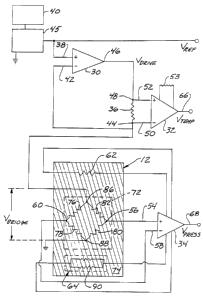
Shown in Figure 2, the signal processing
circuitry 14 comprises a first amplifier 30, a second
amplifier 32, a third amplifier 34 and a sense resistor
36. A non-inverting input 38 of the first amplifier 30
electrically couples to a voltage reference 45 while an
inverting input 42 of the first amplifier 30
electrically couples to a first end 44 of the sense
resistor 36. A power supply 40 provides a stable source
of electrical eneryy to pressure sensor circuit 10. In
the embodiment shown, the voltage reference 45
~ W094~5~ 216 0 4 5 5 PCT~S94/04~79
furthermore produces a stable electrical potential of
2.5 volts to pressure sensor circuit lO. All ~u~u~ ~
of the first amplifier 30 electrically couples to a
second end 48 of the sense resistor 36. Amplifier 30
and sense resistor 36 couple to fo~rm an extremely stable
voltage regulator circuit partly as a result of the
precision and accuracy of the voltage reference device
45. The second amplifier 32, a differential amplifier,
has an inverting input 50 electrically coupled to the
first end 44 of the sense resistor 36 and a non-
inverting input 52 electrically coupled to the second
end 48 of the sense resistor 36. Amplifier 32 has a
predetermined gain factor fixed by the value of a
resistor 53.
The third amplifier 34, a differential
amplifier, has a non-inverting input 54 electrically
coupled to a first node 56 of the bridge circuit and an
inverting input 58 electrically coupled to a second node
60 of the bridge circuit. Third amplifier 34 preferably
is Analog Devices, Inc. part number AMP01/883 or similar
suitable instrumentation quality amplifier that
accommodates two gain-setting resistors for setting the
amplifier gain to a multiple of the ratio of the two
gain-setting resistances. Both a first gain-setting
resistor 62 and a second gain-setting resistor 64
suitably couple to and set the gain of the third
amplifier 34 according to the following equation:
Gain - 20(R62/R6~)-
With reference to Figure 1, an output 66 of
the second amplifier 32 and an output 68 o the third
amplifier 34 electrically couple to an analog-to-digital
converter contained in the signal processing circuitry
14 and then to the microcomputer system 18. In
wog4n~&~ 21 6 ~ 4 ~ ~ PCT~S94104579 -
addition, ~oth the memory 20 and the power supply ~0 are
electrically coupled to the microcomputer system 18.
Ahomogenous, substantiallyflatsemiconductor
substrate 70, shown in detail in Figure 3, includes both
a deflectable portion 72, for supporting the bridge
circuit, and a relatively non-deflectable or rigid
portion 74. In Figure 3, the pressure sensor 12
comprises four pressure sensitive resistors, a first
resistor 76, a second resistor 78, a third resistor 80
and a fourth resistor 82, electrically coupled in a
conventional Wheatstone bridge circuit and supported on
the monolithic silicon substrate 70. The pressure
sensitive resistors are configured in a known manner
such that the resistance of both the first resistor 76
and the third resistor 80 increases as the pressure
exerted on the pressure sensor 12 increases while the
resistance of both the second resistor 78 and the fourth
resistor 82 decreases as the pressure exerted on the
pressure sensor 12 increases. The resistance of each of
20 the pressure sensitive resistors is approximately equal
when no pressure is exerted on the pressure sensor 12.
The silicon substrate 70 further support.s both
the first and second gain-setting resistors, 62,64, on
the relatively non-deflectable portion 74 of the
25 substrate 70, for setting the gain of the third
amplifier 34 as described in detail below. Non-
deflectable portion 74 supports the gain-setting
resistors 62,64 so that in use they are relatively
unaffected by movement of deflectable portion 72 and
therefore, insensitive to applied pressure. Of course,
Figure 3 is illustrative and other arrangements of ~he
elements thereon can be used with the present invention.
Preferably, all of the resistors of the pressure sensor
12 are thin film resistive elements made of polysilicon.
W094125&~ 216 0 4 ~ ~ PCT~S94/04579
In operation, the voltage reference 45
provides a reference voltage, VLCL, to the non-inverting
input 38 of the first amplifier 30, which provides a
driving potential, Vdrive/ at output 46 of the first
amplifier 30. The drive potential causes a bridge
current, Ibridge, to flow through the sense resistor 36
and a constant drive potential, Vbridge, to ~e applied at
a third node 86 of the bridge circuit. The flow of
electrical current through the sense resistor 36
increases until Vbridge equals Vre~ at which point output
46 of the first amplifier 30 stabilizes. The high open
loop gain of first amplifier 30 assures Vbridge will be
held constant at the value of Vref. The bridge current
will flow through the bridge circuit from the third node
86 to a fourth node 88 which is electrically coupled to
a reference potential node. For the embodiment shown,
the electrical grounding is provided by a standard
chassis reference connection to the metal skin and
support structures of an air vehicle. Because Vbrid~ is
held constant, Ibridge varies with the effective bridge
resistance Rbridgel which is temperature dependent and
approximated as follows:
( R76 + R78 ) ( R80 + R82 )
Rbridge = ------------_________
( R~6 + R78 + R80 ~ R82 )
The sense resistor 36 provides a voltage drop
across the inputs 50,52 of the second amplifier 32
proportional to Ibridge The second amplifier 32
amplifies the voltage drop and provides a tempe~-ature
signal V~mp at its output 66 inversely proportional tO
the effective bridge resistance, Rhrl~lq~.
W094/2~ 21~ O ~ ~ ~ PCT~S94/045~ -
As shown, the pressure sensitive resistors
76,78,80,82 typically have a temperature coefficient of
resistance ~TCR) of about 1200 ppm/C. Therefore, the
sense resistor 36 need only have a relatively low TCR in
comparison to the pressure sensitive resistors to ensure
that the sense resistor 36 accurately reflects the
current, Ibridge, flowing through the b~idge.
Accordingly, assuming a pressure sensitive TCR of
1200ppm/C, a TCR of 30ppm/C for the sense resistor 36
will not adversely affect the performance of the
illustrated embodiment of the present invention. As -;
result, Vtemp provides an accurate indication of the
average temperature of the pressure sensitive resistors
76,78,80,82.
As described above, an increase in the
pressure applied to the pressure sensor 12 increases the
electrical resistance of the first and third resistors
76,80 and decreases the electrical resistance of the
second and fourth resistors 78,82. This variation in
resistance induces equal and opposite electrical
potential changes at the first node 56 and the second
node 60. These electrical potential changes couple to
the third amplifier 34 which amplifies the voltage
differential according to the gain equation: Gain =
20(R62/R6.)- The third amplifier 34 provides the
resulting pressure signal, Vpre98, at its output 68.
The analog signals Vtemp and Vpre8~ are provided
to an analog-to-digital converter contained in signal
processing circuitry 14 which provides digital signals
3C to microcomputer system 18 which calculates a corrected
pressure signal, PCorr/ using the following equation
shown in matrix notation:
W094/25~ 216 0 4 5 5 PCT~S94/04579
M00~01~02~03 V
CorrectedP~essure- [lV Y2V3] ~OMllMl2~13 V2
M3O~3lM32M33, Vt,
Where Vp and v, are defined as follows:
Vp- ~ V Vt0~P
Vr~f Vrvr
.
The coefficients comprising matrix M are
calculated at final assembly of the pressure sensor
circuit 10 and stored in the non-volatile memory 20 for
access and use by the microcomputer system 18. These
coefficients are generated by monitoring the pressure
sensor 12 during step changes of temperature and
pressure as is known in the art. The digital circuitry
operates to improve the pressure measurement accuracy by
a-pproximately an order of magnitude, from approximately
1-2% of full scale pressure error to 0.1~ of full scale
pressure error.
In the illustrated embodiment, the pressure
sensitive resistors each have resistance values of lOkQ,
the first gain-setting resistor 62 has a value of
approximately lOkQ, the second gain-setting resistor 64
has a value of approximately 3k~ and the sense resistor
has a value of lkQ. Thus, in the preferred embodiment,
the third amplifier 34 has a gain of approximately 60,
and the output voltage signal for V~p varies from 1.8 to
2 volts and Vpr~, varies from 0.25 to 2.25 volts direct
current.
While the entire bridge current is shown as
passing through the sense resistor 36, it is possible to
design the signal processing circuitry 14 so that only
$~ E S~IEE~ (RU~ ~6)
W094l~&~ - 2 1 6 0 ~ 5 ~ PCT~S94/~79 -
--10--
a fixed or selected portion of the current flowing
through the bridge passes through the sense resistor 36.
In Figure 3, the second gain-setting resistor
64 can contain a trimming ladder 90 which is adjustable
to provide coarse correction for pressure sensitivity
differences between pressure sensors. Following this
adjustment, which is usually made at wafer level during
manufacture, substantially the same processed output
results for the same presEure change affecting a given
batch or group of pressure sensors. This method of gain
adjustment in combination with a zeroing adjustment at
a selected pressure results in interchangeability of
pressure sensors without the need for re-calibration of
the signal processing circuitry 14. As shown, zero
adjustment of the pressure sensor 12 occurs by trimming
dual input resistors 92,94 so that the bridge circuit
balances in the absence of applied pressure.
The term "pressure sensitivity ratio" as used
herein represents the ratio of a change in the amplitude
of an output of the pressure sensor 12 to a change of
applied pressure at a given reference voltage. The
coupling of the first and second gain-setting resistors
62,64 to the third amplifier 34 results in the factory-
set pressure sensitivity ratio being stable over a broad
temperature range. The first and second gain-setting
resistors 62,64 are formed for example by thin film
deposition, doping or other conventional techniques and
are preferably formed simultaneously on the same silicon
substrate as pressure sensitive resistors 76,78,80,82.
Simultaneous fabrication of these circuit components
provides nearly identical temperature ~tracking
performance among all the resistors, partlcularly with
respect to temperature and the effects of aging and use
over long periods of time. Furthermore, although not
W~94l~&~ 216 0 4 5 S PCT~S94/04~79
--11--
shown in the Figures, the gain-setting resistors 62,64
may be deposited close together to optimize linear gain
of the third amplifier 34.
Measuring temperature changes affecting the
bridge circuit by sensing variations in the current
flowing through the bridge circuit requires no separate
temperature detector such as a thermistor. The error
which results from the inherent phase lag of such
detectors under dynamic conditions is eliminated.
Additionally, the present invention provides a
simultaneous measurement of temperature variations and
pressure, even under dynamic temperature conditions and
the illustrated embodiment performs as designed from -
55C to 85C and under continually varying acceleration
forces. Although not shown, a single 5 volt source
could energize the pressure sensor circuit 10, further
reducing the cost and complexity of the present
invention.
Although the present invention has been
described with referenced to preferred embodiments,
workers skilled in the art will recognize that changes
may be made in form and detail without departing from
the spirit and scope of the invention.