Note: Descriptions are shown in the official language in which they were submitted.
216~47~
H.G. van den Brink
Clervauxlaan 10
5625 LC Eindhoven
Optical system for mutually positioning a pad carrying member
and a multileaded component.
With the enhancement of component density on the
printed circuit board and the increasing number of connect-
ions per component, the rejects and cost of rejects will
increase if process control remains unaltered. In parallel
therewith there is a tendency to place the passive and active
components in separate process steps, first the passive
components in a reflow oven/solder bath and, subsequently,
the active components with a system as described.
With state-of-the-art technology, removing a component does
not cause any problem, but the problem arises when the
component is to be positioned or placed back respectively, in
a controlled manner; the leads of the component are to
coincide with minimum clearance with the corresponding pads
on the printed circuit board.
Positioning systems to be used if the problems
outlined above occur are known, it is true, but always have
the drawback of having an extremely complex structure and
being rather costly.
An example of such a system is known from the IBM
Technical Disclosure Bulletin, Vol.34, No.lOB, March 1992,
New York US, pages 4-6; "Precision superposition component
placement tool for end-point sensing".
In contrast, the present invention provides a
system for observing characterized by the features as defined
in Claim 1.
An essential feature of the invention is the
simultaneity of observation, free from parallax, with a large
field of view and a sufficiently high resolution (the human
133HS a3aN3W~
-2160476
eye in combination with a magnifier and/or a binocular
microscope, or in combination with one or more high
resolution cameras, or in combination with a camera) of both
the object (= the foot print of the leads of the multileaded
component) and the pattern of pads to which the leads are to
be fixed.
For considerations of robustness the semi-
transparent mirror used to this end in the invention is
evaporated on a flat transparent substrate which has a finite
thickness. The space behind the semitransparent mirror is
called the image space; the space in front of the mirror, the
observation side and component side, is called the object
space. The mirror substrate having a finite thickness leads
to a displacement of the image space relative to the object
space. The inventive idea is the compensation of this
displacement by the introduction in the object space of a
compensation plate having identical optical properties.
The invention provides two systems for mutually
positioning as claimed in Claims 2 and 3.
According to a first embodiment the centre of the
field of view is selected to be observed at an angle of ~/2.
Depending on ergonomics and desired field of view, object
plane and image plane will form a 20-to-30-degree angle
relative to the beam splitter. The semitransparent mirror
is sandwiched between substrate and compensation plate.
Deviations of the printed circuit board or footprint from
their corresponding surfaces have a marginal effect on the
misalignment after unison. In the case of high-pitch
components, an alternative method of referencing will have to
be implemented.
According to a second embodiment a supporting plate
is chosen which is equidistant to the contact side of the
printed circuit board holder, on the one hand, and, on the
other hand, to the upper surface of the compensation plate
which upper surface likewise functions as the contact area
for the foot print of the component leads, all this in
AMENDED SHEET
216047~
combination with the observation of the lead pattern and the
print at an angle differing from ~/2. If the condition of
equidistance is not fulfilled, this will lead to parallax;
object and image observed at the same angle no longer
coincide after being united (see course of process).
The choice between said first embodiment and said
second embodiment is also made on the basis of the surface
structure of the pad carrying members. If they are not flat,
for example, with warped printed circuit boards (in combin-
ation with high-pitch), it may happen that the printed
circuit board is not located in the theoretical plane of the
contact area of the printed board holder, as a result of
which the leads do not correspond to the footprint (print) of
the component. In that event the first embodiment is strongly
favoured. The second embodiment presents favourable possibil-
ities for high-pitch components on flat substrates.
Side-effects such as the human eye serving as a
detector also play an important role in this invention. In
the first embodiment the object/image plane is perpendicular
to the axis of observation. A binocular microscope can be
applied and is probably desired for the observation of high-
pitch components. In the second embodiment the object/image
plane is at an angle of approximately ~/3 to the axis of
observation. The focusing ability of the human eye enables
the observer to observe sharply every detail within the whole
field of view. People having normal and presbyopic eyesight
observe magnified versions of the details through a low-
magnification magnifier.
The resolution of the human eye, for that matter,
is dependent on the spacial frequency and the contrast
between the objects to be observed. Ambient lighting will
always cause more light to fall on the pad carrying member
than on the under side of the component. A dedicated addit-
ional lighting system provides the necessary contrast between
the pads, on the one hand, and the footprint of the leads, on
the other.
A~ û l~ -T
21~476
.
The invention will be further explained with
reference to the drawings 1 and 2 in which the two
embodiments for the optical system will be shown in a
diagrammatic and simplified manner in connection with the
positioning and locating arrangement. In these drawings:
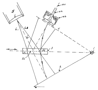
Figure 1 gives a diagrammatic representation of a
cross-section of a system according to a first solution. The
displacement of the component towards the pad carrying member
is effected by a rotation around axis 1. The pad side of the
pad carrying member is fixed in plane 2, the imaginary plane
of the footprint of component 4.1 lies in plane 4, the semi-
transparent mirror lies in plane 3.2; the three planes 2, 3.2
and 4 meet in axis 1 while the angles between the planes are
mutually equal. The beam splitter assembly 3 comprises the
semitransparent mirror 3.2, the mirror substrate 3.1 and the
compensation plate 3.3. Observation takes place through
magnifier 5, arranged in such a way that the optical axis 6
of the lens means is perpendicular to the centre of the field
of view i.e. in the centre line 4.4 of the component fixing
means. The component 4.1, the component fixing means 4.2 and,
if required, the heating means 4.3, are shown in a
diagrammatic way. Depending on ergonomics and desired field
of view, the object plane and image plane will form an angle
of approximately 30 degrees relative to the beam splitter. By
displacing the printed circuit board in the directions of X
and Y and rotating the component fixing means, the images of
the pads and the connecting leads are arranged to be
superimposed.
The beam splitter assembly is then reproducibly
removed from the path of the component. The component fixing
means holding the component is turned onto the printed
circuit board in a rotating manner.
Figure 2 represents a system according to a second
solution in which the reference plane 8 is the contact plane
of the pad carrying member. Perpendicular thereto is the axis
of displacement 10.4 of the component. The beam splitter
A~qF ,, ~
- 216Q476
assembly 9 comprises the semitransparent mirror 9.2, the
mirror substrate 9.1 and the compensation plate 9.3 the upper
surface of which compensation plate made of quartz
functioning as a contact plane for the footprint of the
connecting leads of the component lO.l. Mirror substrate and
compensation plate should be adjusted to be perfectly in
parallel. The angle of the beam splitter assembly should be
adjustable, so that the beam splitter can be adjusted in
parallel with the contact plane of the pad carrying member.
The beam splitter assembly is height-adjustable so as to
satisfy the condition of equidistance of the contact side of
the printed board holder to the semitransparent mirror, on
the one hand, and to the upper surface of the compensation
plate, on the other. With the selected configuration there is
achieved that, once the connecting leads have been aligned to
the corresponding pads - once the splitter assembly has been
removed in a reproducible manner - and the leads have been
displaced vertically, these leads will coincide with the
corresponding pads. The magnifier 11 with optical axis 6 is
adjusted, so that the plane of focus 11.1 lies within the
field of view behind the printed circuit side of the pad
carrying member.
4 ~ r 1 `, . _ _ _