Note: Descriptions are shown in the official language in which they were submitted.
2160500
BC9-94-185
A PCI/ISA BRIDGE HAVING AN ARRANGEMENT FOR RESPONDING
TO PCI ADDRESS PARITY ERRORS FOR INTERNAL PCI SLAVES
IN THE PCI/ISA BRIDGE
BACKGROUND OF THE INVENTlON
Field of the Invention
The present invention relates to the field of digital computer systems, and more10 particularly, to master-slave transactions on a PCI bus.
io~ of Related Art
In computer systems, electronic chips and other components are connected with one
another by buses. A variety of components can be connected to the bus providing
15 intercommunication between all of the devices that are connected to the bus. One type of
bus which has gained wide industry acceptance is the industry standard architecture (ISA)
bus. The ISA bus has twenty-four ~24) memory address lines which therefore provides
support for up to sixteen (16) mcgabytes of memory. The wide acceptance of the ISA bus
has resulted in a very large pcrcentage of devices being designed for use on the ISA bus.
20 However, higher-speed input/output devices commonly used in computer systems require
faster buses.
A solution to the general problem of sen(ling and receiving data from the processor
to any high-speed input device is a local bus. Unlike Ihe ISA bus, which operates relatively
slowly with limited bandwidth, a local bus communicates at system speed and carries data
25 in 32-bit blocks. Local bus machines remove from the main system bus those interfaces that
need quick response, such as memory, display, an<l disk drives. One such local bus that is
gaining acceptance in the industry is the peripheral component interconnect (PCI) bus. The
PCI bus can be a 32 or 64-bit pathway for high-specd data transfer. Essentially, the PCI
bus is a parallel data path provided in addition to an ISA bus. The system processor and
2160500
BC9-94-185 2
memory can be attached directly to the PCI bus, for example. Other devices such as graphic
display adapters, disk controllers, etc. can al,o attach directly or indirectly (e.g., through a
host bridge) to the PCI bus.
A bridge chip is provided between the PCI bus and the ISA bus in order to provide
5 communication between devices on the two buses. Tlle bridge chip essentially translates the
ISA bus cycles to PCI bus cycles, and vice versa.
Many of the devices attached to the PCI bus and the ISA bus are master devices that
can conduct processing independently of the bus or other devices. Certain devices coupled
to the buses are considered to be slaves or targets that accept commands and respond to
10 requests of a master. According to the PCI protocols, set forth in the PCI specification
(herein incorporated by reference) a PCI slave needs to respond to a master that requests
a transaction with that slave within a certain predetermined time period, for example, five
clocks after the PCI master has asserted a frame signal.
In a normal PCI transaction, the PCI master will assert a frame signal (FRAME#)
15 along with an address signal and address parity information. The PCI slave coupled to the
PCI bus will decode the address after detecting the frame signal on the PCI bus to determine
if the slave is being addressed by the PCI master. If the PCI slave determines that it is being
addressed by the master, it will assert a device selcct signal ~DEVSEL#) to claim the cycle.
At the same time, however, the slave compares the parity address information with the
20 address asserted by the PCI master. lf an address parity error is detected by this PCI slave,
it can perform a master-abort, perform a target-abort by deasserting the device select signal
DEVSEL# and asserting a stop signal (STOP#), or i~nore the parity error. The target-abort
ends the master-slave transaction cycle even if the master intended the transaction to be
performed with a different slave and that different slave was able to respond to the
25 transaction.
A PCI master can also perform a master-abort, and does so when it fails to receive
a device seleet signal DEVSEL# from a PCI slave within a certain time period after the
assertion of FRAME# by the PCI master. The predetermined time period can be five clock
cycles after the assertion of FRAME#, for example. The failure to receive a device select
2160500
BC9-94- l 85 3
signal DEVSEL# indicates that no PCI slave has claimed the cycle so that the PCI master
will effeetively end the master-slave transaction cycle.
The bridge chip interfacing between the PCI bus and the ISA bus ean be eonfigured
to eontain elements operating as PCl slaves. However, a problem with such an arrangement
5 is that the PCI slaves on the bridge chip must respond to the FRAME# on the PCI bus
within the time limits defined by the protocol of the PCI bus. This is particularly
troublesome when the bridge chip is a relatively low-speed chip. In order to provide the
response to the PCI master within the speciried time period, the PCI slave within the bridge
ehip must respond as a fast PCI device by asserting the device select signal within the eloek
10 eyele after reeeiving the FRAME#. The bridge chip would then assert in the following cycles
the deviee seleet signal DEVSEL# to the PCI bus and the PCI master. Once a device seleet
signal DEVSEL# is asserted by a PCI slave, a master-abort termination is not possible, only
a target-abort.
It is possible, however, due to parity error~ that the PCI slave within the bridge ehip
15 is not the intended target of the PCI master for the master-slave transaction. In sueh a case,
a target-abort is inappropriate sinee the master-slave transaetion is meant for another slave
whieh eould possibly still elaim the address. The bridge therefore performs an address parity
error eheek using the address and the address parity information provided by the PCI
master. If the bridge determines that there is an address parity error, it will provide an
20 address parity error signal to the PCI slave within the bridge. Because of the fast response
required by the PCI protocol, however, the PCI slave needs to assert the device select signal
DEVSEL# within a time period before the bridge can check for the address parity error and
generate the address parity error signal to the PCI slave on the bridge. There is therefore
a dilemma created by the requirement of asserting the clevice select signal DEVSEL#
25 internally by the PCI slave such that a response can be made to the master within the
predetermined time period for PCI transactions, and preventing the PCI slave within the
bridge from generating a target-abort on the PCI bus since another slave may be the
intended target.
2160500
BC9-94-185 4
SUMMARY OF THE INVENTION
There is a need for a method and a system using a PCI bridge having PCI slaves that
respond within the predetermined time period to frame signals asserted by PCI masters,
without requiring target-aborts to be generatcd on the PCI bus in response to an address
parity error.
These and other needs are met by the present invention which provides a bridge for
interfacing between buses of a computer system having first and second buses and a master
coupled to the first bus that asserts an address and address par;ty information on the bus
to initiate a master-slave transaction over the first bus. The bridge comprises logic for
comparing the address and the address parity information and generating an address parity
error signal when there is a parity address error. A slave in the bridge receives the parity
address error signal and generates a target-abort signal in response. The bridge also has logic
for preventing the target-abort signal from propagating to the first bus.
The earlier stated needs are also met by another embodiment of the present invention
which provides a computer system comprising first ancl second buses, a master coupled to
the first bus which asserts an address and parity information on the bus to initiate a master-
slave transaction over the first bus. A bridge is coupled between the first and second buses.
This bridge includes logic for comparing the address and the parity information and
generating an address parity signal when there is an address parity error. The bridge also
includes a slave that receives the address parity error signal and generates a target-abort
signal in response, and logic for preventing the target-abort signal from propagating to the
first bus.
In preferred embodiments, the rirst hus is a PCI bus, all(l the master is a PCI master
and the slave is a PCI slave.
The present invention pr(lvides the advantage of allowing the PCI slave within the
bridge to respond within the time periods specified by the PCI bus protocol, since the bridge
simultaneously determines if there is an address parity error and prevents the target-abort
signal (the device select signal and the stop signal) from being propagated out of the bridge
chip in the event that there is an address parity error.
2160500
BC9-94- 185 5
The foregoing and other objects, features, aspects and advantages of the presentinvention will become more apparent from the following detailed description of the present
invention when taken in conjunction with the accompanying drawings.
5 BRIEF DESCRIPTION OF THE DRAWINGS
Figure 1 is a perspective view of a computer of a computer system of the presentinvention.
Figure 2 is a block diagram with a computer system of Figure l constructed in
aecordanee with an embodiment of the present invention.
Figure 3 is a bloek diagram of the address parity error and PCI signal generation
element of the bridge constructed in accordance with an embodiment of the present
mventlon.
Fiigure 4 is a timing diagram of an address parity error response in which an external
PCI master-abort is formed from an internal PCI target-abort in accordance with a method
15 of the present invention.
DESCRIPTION OF THE ILLUSTRATIVE EMBODIMENTS
With reference now to the Figures and in particu]ar with reference to Figurc 1, a
conventional computer, or PC, designaled 10, is of the environment to which the invention
20 has particular utility. Computer 10 which preferably, but not necessarily, is of a type
utilizing an IBM personal computer Ot a similar system, includes a console housing 12 in
which a circuit board containing the necessary circuitty including a microprocessor and
BIOS chips, controllers, random access memory an(l other hardware are arranged. The
computer will also include a vide(I disl-lay 14 and a keyboard l~ connected to the housing
25 12 through cable l~. Mass storage media includes a hard disk drive within the housing and
is non-accessible to the user, and user-accessible flOppy disks, as well as, optionally, CD-
ROM drives 20 and 22.
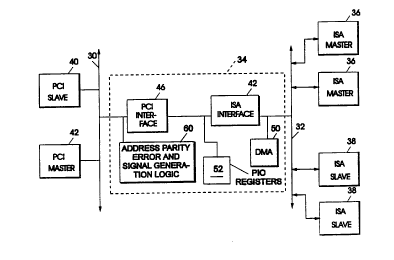
Figure 2 is a block diagram of a computer system constructed in accordance with an
embodiment of the present invention. The system includes a PCI bus 30, an ISA bus 32,
21605 0 0
BC9-94- l 85 6
with a plurality of ISA masters 36 and ISA slaves 3X. A plurality of PCI memory slaves 40
are coupled to the PCI bus 30.
The bridge chip 34 contains an ISA interface 42 coupled between the ISA bus 32 and
a system bus 44. A PCI interface 46 is provided between the PCI bus 30 and system bus 44.
The bridge chip 34 also has a DMA controller 50, programmable l/O (PIO) registers 52 and
address parity error and PCI signal generation logic 6() that will be described later. The
DMA controller 50 is coupled to the ISA bus 32. The bridge chip 34 provides an interface
between the PCI bus 30 and the ISA bus 32.
The ISA bus interface 42 in the bridge chip 34 translates ISA bus cycles into a system
bus cycle for use by the bridge chip 34. The PCI bus interface 46 converts PCI bus cycles
from the PCI bus 30 into system bus cycles for the bridge chip 34. The DMA controller 50
controls DMA control of memory accesses within the syslem. The DMA controller 50provides a plurality of separate DMA channels over which memory accesses involving the
individual ISA masters 36 are respectively communicated.
Either the DMA controller 50 or the ISA bus master 36 can generate transfer cycles,
since the DMA controller 50 acts as a bus master on the ISA bus 32. Both the ISA master
36 and the DMA controller 50 can access memory located on either the ISA bus 32 or the
PCI bus 30. For ease of explanation in the following description, however, examples will be
described in which the ISA bus master 36 is generating transfer cycles. When this occurs,
the DMA controller 50 acts as an arbitration device.
Figure 3 is a block diagram of the address parity error and PCI signal generation
logic 60 depicted in the bridge chip 34 in the system of Figurc 2. The logic 60 includes a
plurality of PCI slaves 62, in this example, that are coupled to an internal latched PCI bus
63. ~n internal PCI input and output latch an<l PCI interface logic 64 (hereinafter "PCI
latch and interface logic 64") is coupled between the PCI bus 30 and the internal latched
PCI bus 63. The PCI latch and interface logic 64 receives the signals from the PCI bus 30
and the internal latched PCI bus 63 and latches these signals for use by the bridge 34 and
the logic 60. Latches are needed since the PCI bus 30 operates at a high speed and PCI
slaves 62, implemented in a slow technology, cannot reliably operate with unlatched signals.
2160500
BC9-94- 185 7
The PCI latch and interface logic 64 receives from the PCI bus 30 the address signals,
the frame signal (FRAME#), the IRDY# (initiator ready) signàl. The logic 64 sends the
device select signal (DEVSEL#), the stop signal (STOP#), and target ready signal (TRDY#).
Latched versions of each of these signals on the internal latched PCI bus 63.
The address from the PCI bus 30 is also received by an address parity generator and
check logic 66. In addition to the unlatched address, the address parity generator and check
logic 66 (hereinafter the "check logic 66"~ receives unlatched parity information from the PCI
bus 30. The unlatched parity address information and the address are compared, and if
there is an error, the check logic 66 changes the level of the internal bridge address error
signal (PIB_ADD_ERR). This signal is Iatched at a separate latch 6X, where it is available
to the PCI slaves 62.
A basic description of the operation of the adclress parity error and PCI signalgeneration logic 60 will be described, ~ith a more detailed clescription of an address parity
error response, including a timing diagram, following this brief description.
When a master 42 desires to perform a master-slave transaction with one of the PCI
slaves 62, the master 42 asserts FRAME#, an address, and address parity information on
the PCI bus 30. The address parity error and PCI signal generation logic 60 on the bridge
34 receives FRAME# and the acldress information in the internal PCI latch and interface
logic 64 where it is latched for use in the bridge chip 34. The latched FRAME# and address
signals are placed onto the internal PCI bus 63 where they are available to the PCI slaves
62. The PCI slaves 62 decode the latched acldress and determine whether the particular PCI
slave 62 is to respond to the master 42. One of the PCI slaves 62, assuming that decoding
indicates that this particular PCI slave 62 is to respond, asserts a device select signal
DEVSEL# on the internal latched PCI bus 63. T he internal PCI latch and interface logic
64 asserts the device select signal DEVSEL# on the PCI bus 30 where it is received by the
master 42. The particular transaction is then performecl when the IRDY# and TRDY# are
both asserted.
All of the above operational description assumes that the address and address parity
information check has not caused an address parity error signal to be generated. This
2160500
BC9-94- 185 8
cheeking is performed at the same time as the address is being decoded by the PCI slaves
62.
Assume, however, now that the address parity information check performed by the
eheck logic 66 indicates that there is an address parity error. Also assume that one of the
PCI slaves 62 has claimed the address by as~serting DEVSEL#. The check logic 66 asserts
the internal bridge address parity error signal (PIB_ADD_ERR) where it is latched by latch
68. The latched address parity error signal is sent to the PCI ~slaves 62. The PCI slave 62
that claimed the address then performs a target-abort of the master-slave transaction. This
is accomplished by the deassertion of the device select signal DEVSEL# and the assertion
of the stop signal STOP# by the PCI slave 62. The latched internal bridge address parity
error signal is provided to the internal PCI latch and intert`ace logic 64, which has also
received a device select signal. When the internal PCI latch and interface logic 64 has
received both the latched address parity ertomsignal, and the device select signal DEVSEL#,
the logic 64 blocks both the device select ~signal DEVSEL# and the slave stop signal STOP#
from propagating (being latched) to the PCI bus 30. The target-abort is therefore not seen
on the PCI bus 30 by the master 42. If no other slave on the PCI bus 30 claims the address
by assertion of a device select signal DEVSEL# within a predetermined time period after the
master 42 asserted FRAME#, the master 42 will pelform a master-abort.
It should be recognized that the device select signal DEVSEL# assertion could not
be delayed by the PCI slave 62 until the unlatched internal bridge address parity error
information is decoded since the PCI bus protocol requires that the PCI slave 62 responds
internally with a fast response (in the first clock ~rter a.ssertion of FRAME#) so that the
external response, which is a slow response (in the thircl clock after assertion of FRAME#),
is possible within the time con.straints of the PCI bus protocol.
A more detailed explanation of the address parity error response by the arrangement
of the present invention will now be de~scribecl with reference to the timing diagram of Figure
4.
The master 42 asserts the frame signal FRAME# and lhe address information in
clock l. This information is latched in the PCI latch and interface logic 64 in clock 2.
2160500
BC9-94- l 85 9
During clock 2, the address parity information is received from the master 42. This
information is compared with the adclress by the check logic 66 during clock 2. At the same
time that the check logic 66 is checking the parity information, the PCI slave 62 sees the
asserted latched FRAME# and decodes the latched address.
In this example, the comparison by the check logic 66 of the address parity
information with the address ind;cates an address parity error. The check logic 66 therefore
generates an internal bridge address parity error signal (PIB_ADD_ERR~ at the end of
clock 2. This signal is latched (LATCHED PIB_ADD_ERR) in clock 3. However, the PCI
slave 62, which has decoded the address, responds to the latchecl FRAME# in clock 3 in
order to meet the timing requirement.s of the PCI bu~s 30 by asserting the device select signal
DEVSEL#. The PCI slave 62 therefore operates internally as a "fast" PCI slave since it
responds within one cycle after receipt Or the latche-l FRAME#. To the PCI master 42,
however, which receives the device select signal DEVSEL# from the slave 62 (when there
is not an address parity error) three cycles after the assertion of the frame signal FRAME#,
the PCI slave 62 is a "slow" slave.
By clock cycle 4, the PCI slave 62 recognizes the latched address parity error signal
(the PIB_ADD_ERR signal) and performs an internal target-abort by deasserting the device
select signal DEVSEL# and asserting the stop signal STOP#. This effectively stops the PCI
slave 62 from performing the master-slave transaction. The PCl latch and interface logic 64
has prevented the device select signal DEVSEL# and the stop signal STOP# from
propagating onto the PCI bus 30 as a target-abort where it would be seen by the master 42.
The PCI latch and interface logic 64 blocks DEVSEL# and STOP# in response to receipt
of the latched PIB_ADD_ERR (latched addre.ss pal^ity error signal) from the latch 68 and
the device select signal DEVSEL# asserted hy the PCI slave 62. Externally, the PCI device
select signal DEVSEL# remains deasserted (at a high Icvcl), and tlle PCI stop signal STOP#
also remains deasserted, as seen in the masked signals in ~igurc 4. Another slave on the PCI
bus 30 is able to claim the address, Or the external PCI mastel 42 will perform a master-
abort if it does not receive a device select signal DEVSEL# from another PCI slave on the
PCI bus 30.
21605~U
BC9-94- 185 10
Without the present invention, thc PCI device select signal DEVSEL# would be
asserted on the PCI bus 30 as shown hy the unmasked signals at the bottom of Figure 4,
followed by a PCI stop signal STOP# in clock 5. This ~ould undesirably force a target-abort
on the PCI bus 30.
With the arrangement and method of the present invention, the required master-abort
termination of an address parity error is performed by the bridge chip 34, even though a
target-abort mechanism is used to meet the technology/timing requirements internally. This
allows the synthesis of the bridge chip in a slower, Iess expensive technology than would
otherwise be possible.
The target-abort generated internally from the latched parity internal bridge address
parity error information signal ensures that in worst case boundary conditions, the internal
PCI slave 62 will guarantee proper state machine control. If the unlatched address parity
error signal were used to perform a master-abort internally, under worst case eonditions,
unpredietable behavior would result.
Although the present invention has been described and illustrated in detail, it is
elearly understood that the same is by way of illustration and example only and is not to be
taken by way of limitation, the spirit and scope of the present invention being limited only
by the terms of the appended claims.