Note: Descriptions are shown in the official language in which they were submitted.
~ 94/~759 21 G a ~ 9 2 - 1- PCT~S94/04100
BALANCED MODULATOR-TRANS~~
CRQSS-REFERENCE TO RELATED APPLICATIONS
The present patent application has the same Assignee as
U.S. Patent Application Serial No. 07/924,525, filed August
4, 1992, and is related to U.S. Patent No. 4,804,931, issued
February 14, 1989. Both documents are incorporated herein by
reference.
BACKGROUND OF THE lNV~llON
1. Technical Field
The present invention relates to modulators. More
specifically, the invention relates to balanced modulators
(those having no carrier component in the output waveform),
especially balanced quadrature amplitude modulation (QAM)
modulators.
2. Bac~oul-d Art
In U.S. Patent No. 4,804,931 (which is incorporated
herein by reference in its entirety), a digital amplitude
modulator-transmitter is described. An amplitude modulator-
transmitter embodying the teachings of the '931 patent is
illustrated in FIG. 1.
The amplitude modulator 30 includes a predetermined
number of quadrature hybrid power devices 32l-32n. The
quadrature hybrid power devices 321-32n are configured as
combiners, and are arranged in cascade so that the output of
one combiner is the first of two inputs of a successive
combiner. In the exemplary illustration of FIG. 1, only four
combiners are shown for ease of understanding.
The construction and operation of a quadrature hybrid
device is described in detail in the '931 patent, and need not
be described here. However, for purposes of the present
discussion, a quadrature hybrid combiner may be implemented
as a four-port device having first and second inputs, one
output, and one isolated port. The first and second inputs
receive two signals of a given amplitude that are 90- apart
in phase. The input signals are combined to provide an ouL~uL
signal having an amplitude that is the sum of the amplitudes
of the input signals. As shown in FIG. 1, ports l and 4
~UæSlllUl~ SHEEr (RULE 2B)
W094/~7S9 2 ~ 6 0 S 9 ~ -2- PCT~S94/04100 -
represent the first and second input ports. Port 3 represents
an isolation port to which is attached a resistor representing
a dummy load 34. Finally, port 2 defines the output port of
each of the combiners.
An analog signal source 36, such as a microphone or a
video generator, produces an analog signal that passes through
an analog-to-digital converter (A/D converter, or ADC) 38.
The digital output of the A/D converter appears on data
lines 40.
As an example, there are four data lines, so that data
consists of four-bit words. However, it is contemplated that
12- or 16-bit words may be employed to improve the quality of
the signals being transmitted. Further, it is contemplated
that a digital input signal may be fed directly to gates 42
without the need for A/D converter 38, should the modulating
signal already exist in binary form.
Each of the bits, from the least significant bit tLSB)
to the most significant bit (MSB), controls a respective gate
421-42n- Each of the gates is connected in series with a
corresponding amplifier 441~44n. The series combinations
receive an RF signal from an RF signal generator 46, and
provide respective s co~ inputs to the combiners.
The o~uL port of the LSB combiner 321 represents the
least significant bit of the digital word describing the
instantaneous value of the signal to be modulated. The second
input of the combiner 322, adjacent the LSB combiner 32l,
represents a value that is twice as significant as that of the
second input of the LSB combiner 321. Similarly, the second
input of each successive combiner represents a value twice as
significant as that input to the immediately prece~ing
combiner.
Thus, the ouL~- of each combiner represents a binary
weighted power signal. In particular, the signal appearing
at the ou~uL of the MSB combiner 42n represents the sum of
the power signals fed into the various combiners. This o~u~
signal is fed for transmission to a load, typically an antenna
with conventional filtering.
The modulator-transmitter in the '931 patent has many
advantages, such as its ability to provide pseudo-continuous
amplitude modulation at any modulation index ~etween 0 and 1,
S!J~ S~T (R~E 26)
~ 94l~759 21 60~ 2 3 PCT~S94/04100
at any carrier frequency, using any one of the wide variety
of classes of amplifiers. However, it is not a balanced
modulator, as a carrier component is present in the output
waveform. Thus (assuming a sinusoidal modulating signal of
S angular frequency ~), the digital amplitude-modulator
described in the '931 patent provides an output signal which
may be represented as:
s~(t)=A(l+cos ~t)(cos ~ct) (1)
where:
s~(t) is the output of the amplitude modulator;
A is a constant;
~8 is the modulating signal angular frequency:
~c is the carrier signal angular frequency; and
t is the variable for time.
As will readily be appreciated by those skilled in the art in
light of the '931 disclosure, a carrier frequency component,
and symmetrical upper and lower sidebands, are present in the
output signal.
For various reasons appreciated by those skilled in the
art, suppression of the carrier is often desirable. In
particular, in formats which may be used for high definition
television (HDTV) and digital cellular telephone systems,
suppression of the carrier is required.
Generally, a balanced modulator provides an ouL~u~ having
no carrier, and may be expressed by the formula:
s~(t)=A(cos ~,t)(cos ~ct) (2)
This formula assumes that the modulating waveform is
sinusoidal in form with an angular frequency of ~,. More
generally, a balanced modulator receiving an arbitrary
modulating waveform a(t) having no DC component provides an
o~L~u~ that can be described by the formula:
SB~ (t)=A(a(t))cos ~ct (3)
However, the '931 patent does not describe a manner in which
a balanced modulator may be implemented. It is to meet this
need that the present invention is directed.
Various patents are directed to modulators. For example,
U.S. Patent No. 5,153,536 (Muller) discloses a QAM modulator
having an arrangement of double modulators and partial
modulators. U.S. Patent No. 3,757,222 (Oberbury) discloses
a single sideband generator involving selective switching of
SU~SIllUltShttl (RUlE26)
W094/~759 -4- PCT~S94/04100 -
transmission line links. U.S. Patent No. 4,635,004 (Ishigaki)
discloses a single sideband generator in which quarter-wave-
shifted signals are alternately input to a balanced modulator.
U.S. Patent No. 4,717,894 (Edwards et al.) discloses a method
of calibrating a vector modulator involving in-phase and
quadrature components. Finally, U.S. Patent No. 4,068,l00
(Thompson) discloses an AM stereo system in which opposite-
polarity half-cycles of a carrier are separately modulated
with a different channel. However, none of the existing art
is believed to provide all the advantages of the present
invention.
DISCLOSURE OF THE I~v~llON
The invention provides various embodiments of a balanced
modulator, each of which involves one or more individual
amplitude modulators which, individually, do not provide
suppressed-carrier ~L~u~s. A first embodiment employs a
single amplitude modulator whose carrier input is selectively
delayed by a half wavelength, depending on the polarity of the
input modulating signal, and whose amplitude input receives
the absolute value of the modulating input signal. A second
embodiment involves summation of the ouL~uLs of two amplitude
modulators whose carrier inputs are responsive to carrier
signals offset by a half carrier wavelength and whose
modulating signal inputs are responsive only to signals of
respectively opposite polarity. Further, quadrature amplitude
modulation (QAM) modulators are provided by a combination of
the above-described modulators. Moreover, another embodiment
of the QAM modulator involves use of an amplitude modulator
operating on polar coordinate representation~ of the input
modulating signal. The invention is useful in single sideband
modulation, up-conversion, down-conversion, synchronous
detection, product detection and the like.
.
BRIEF DESCRIPTION OF DRAWINGS
The invention is better understood by reading the
following Detailed Description of the Preferred Embodiments
with reference to the accompanying drawing figures, in which
like reference numerals refer to like elements throughout, and
in which:
SU8STITIJTE SHEET tRULE 26)
~ 94/~759 1 60S9~ PCT~S94104100
FIG. 1 illustrates an amplitude modulator constructed in
accordance with the teachings of U.S. Patent No. 4,804,931.
FIG. 2 illustrates a first embodiment of the balanced
modulator according to the present invention.
FIG. 3 illustrates a second emboAim~nt of the balanced
modulator according to the present invention.
FIGS. 4A and 4B illustrate quadrature amplitude
modulators employing balanced modulators according to the
embodiments of FIGS. 2 and 3, respectively.
FIG. 5 illustrates a further embodiment of a quadrature
amplitude modulator according to the present invention.
FIG. 6 illustrates an exemplary single sideband modulator
employing balanced modulators according to the present
invention.
FIG. 7 illustrates an exemplary single si~h~n~
quadrature amplitude modulator according to the present
invention.
R~T MODES FOR C~RRYING OUT THE lN V~N'l'lON
In describing preferred embodiments of the present
invention illustrated in the drawings, specific terminology
is employed for the sake of clarity. However, the invention
is not inten~e~ to be limited to the specific terminology so
selected, and it is to be understood that each specific
element includes all t~chnical equivalents which operate in
a similar manner to accomplish a similar purpose.
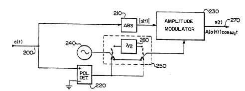
Referring now to FIG. 2, a first balanced modulator
according to the present invention is illustrated. The input
modulating waveform a(t) is input to the modulator on
path 200. Path 200 leads to an absolute value functional
block 210 and a polarity detector 220. The absolute value
functional block 210 provides the instantaneous absolute value
of a(t) to the modulating data input of a digital amplitude
modulator 230. Preferably, the modulator 230 is implemented
as the digital amplitude modulator described in the U.S.
Patent No. 4,804,931, described above, with reference to
FIG. 1. Modulator 230 provides an output of the type
described above, in Formula 3.
Polarity detector 220 provides a binary GuL~uL, depending
on the polarity of the input modulating signal a(t). The
Su~s~ Jltshttl (RULE26)
W094/~759 ~6~9~ PCT~S94/04100 -
-6-
binary output of polarity detector 220 is input to the control
input of a switch arrangement 250. The switch arrangement 250
receives a single input, from a carrier generator 240 which
produces a signal A cos ~t. The switch arrangement 250
provides a carrier output to modulator 230.
Referring briefly to FIG. 1, it is understood that the
data input to modulator 230 tFIG. 2) corresponds to the signal
between elements 36, 38, and that the carrier input from
switch arrangement 250 (FIG. 2) corresponds to RF signal
generator 46 (FIG. 1).
Referring more specifically to the details of elements
within FIG. 2, polarity detector 220 may be implemented
through use of a voltage comparator having a non-inverting
input and an inverting input. The modulating input signal
a(t) is provided to the non-inverting input, and the inverting
input is connected to ground. The comparator's binary o~L~u~
is a first logic state (for example, 1) when a(t) is greater
than zero, and the ouL~uL is a second value (for example, 0)
when a(t) is less than zero volts.
Swit~hin~ arrangement 250 may be implemented as a double
pole, double throw switch implemented using gallium arsenide
(GaAs) switches which selectively connect, or disconnect, a
delay element 260. This delay element may be in the form of
a transmission line equal to half the wavelength of the
carrier wave. In the illustrated example, when the output of
polarity detector 220 is zero, the switches in switch
arrangement 250 are connected in the manner illustrated, so
as to bypass the half-wavelength delay element 260.
Conversely, when polarity detector 220 ouL~u~s a 1, the
switches connect the opposite poles, so that the half-
wavelength delay line 260 is interposed between carrier
generator 240 and modulator 230.
Finally, the absolute value function 210 may be
implemented according to any suitable configuration, as
readily appreciated by those skilled in the art. For example,
it may be implemented using a precision full wave rectifier.
The elements in FIG. 2 may be implemented differently
than as specifically described above, while still remaining
within the scope of the present invention. In any event, the
SUBSTITUTE S~IEET (RULE ~)
9t~759 60~92 _7_ PCT~S94/04100
modulator of FIG. 2 provides a double sideband suppressed
carrier modulation output.
A second embodiment according to the present invention
is shown in FIG. 3. The FIG. 3 embodiment employs a duplicate
modulator instead of employing a switching arrangement such
as that in the FIG. 2 embodiment.
Referring to FIG. 3, the input modulating signal a(t) is
input to schematically illustrated clipping circuits 310, 320.
Clipping circuit 310 provides an output only when a(t) is
greater than zero. Conversely, clipping circuit 320 provides
an output only when a(t) is less than zero. Clipping circuits
310, 320 provide their outputs to respective modulators 3301,
332- Preferably, these modulators are implemented as the
digital amplitude modulator disclosed in U.S. Patent No.
4,804,931, described with reference to FIG. 1. It is
understood that the modulating inputs to the FIG. 3 modulators
correspond to the signal between elements 36, 38 in FIG. 1.
Referring again to FIG. 3, a carrier generator 340 is
provided, connected to a half-wavelength delay element 360.
First modulator 330l receives the output of carrier generator
340 directly, whereas second modulator 330z receives the half-
wavelength delayed carrier from delay element 360. It is
understood that the carrier inputs in the FIG. 3 modulators
correspond to the RF signal generator 46 (FIG. 1).
Modulators 330l and 332 provide respective outputs to a
summing element (adder) 370, whose output may be expressed as
the generalized balanced modulator Formula 3, provided above.
Adder 370 adds the outputs of the two modulators, but it is
recognized that, at any given instant, at least one of the
modulators will have zero output due to the operation of
clipping circuits 310, 320. By implication, the ultimate
GuL~uL of the system, stt), is the output of the one modulator
which is active at any given instant.
The illustration of clipper elements 310, 320 is
schematic in nature, and is used for purposes of explanation.
In a practical embodiment, each modulator 330l~ 332 would
have its own analog-to-digital converter (ADC) at its input.
The first modulator's ADC (element 38 in FIG. 1) is configured
to respond with measurable (non-zero) ouL~uL only when its
input is greater than zero. Conversely, the second
S~ SHEEr (RULE ~6)
W094/~759 ~ ~60S9 -8- PCT~S94/04100 -
modulator's ADC provides non-zero output only when the
modulating input wave form a(t) is less than zero. In this
manner, actual analog clipping elements 310, 320 are avoided.
As described in the '930 patent, each of the individual
modulators 230, 3301, 332 (FIGS. 2-3) may take advantage of
the high efficiency of non-linear RF amplifiers while still
providing a linear amplitude-modulated signal at signal levels
high enough for transmission. The present invention builds
on the advantages of that modulator by exploiting its
efficiency and high signal levels. Moreover, present
inventionprovides apparatus forsuppressed-carriermodulation
and trAn~;csion which is especially suitable for various
st~n~rdized transmission formats. A notable example is
quadrature amplitude modulation (QAM).
QAM modulators provide ou~u~ in which two carriers,
differing in phase by one-quarter wavelength, are suppressed.
Usually, the modulating signal input to QAM modulators include
a ~eries of pairs of pulses, with the average DC value of each
pair of pulses being zero. Advantageously, the present
invention provides a QAM modulator which can modulate any
arbitrary input waveform having no DC component, even those
not of the paired pulse st~nA~rd.
FIGS. 4A and 4B show QAM modulators employing the
teachings of the embodiments of FIGS. 2 and 3. The input
modulating signal is provided in ~he form of in-phase and
quadrature components a (t) and aQ(t), respectively. These
in-phase and quadrature signals are input to the modulating
inputs of respective modulators 420, 430. In FIG. 4A, the
modulators 420, 430 are indicated as being of the type shown
in FIG. 2 (excepting the carrier generator). Similarly,
FIG. 4B indicates the modulators 420, 430 being of the type
shown in FIG. 3 (again, excepting the carrier generator).
The modulators 420, 430 receive their respective carrier
inputs from a carrier generator 440 and from a quarter-wave
delay element 460. The modulators 420, 430 provide ouL~uLs
to a summing device 470. Summing device 470 provides the QAM
modulated o~u~ signal.
S~8STITUTE SHEET (RULE 26)
~ 21 6 0 ~9 2 PCT~S94104100
The QAM output signal may be of the form described by the
following formula:
sQ~(t)=A[aI(t) cos ~ct + aQ(t) sin ~ct] (4)
where:
A is a constant;
aI(t) is the in-phase component of the modulating signal;
aQ(t) is the quadrature component of the modulating
signal;
a(t) equals aI(t) plus aQ(t);
~c is the carrier angular frequency;
t is the variable for time; and
aI(t) and aQ(t) can take on positive or negative values.
Referring now to FIG. 5, still another quadrature
amplitude modulator according to the present invention is
illustrated. The invention of FIG. 5 builds on the advantages
of the embodiments of FIGS. 2-4, and provides additional
benefits relating to power savings and lower required Nyquist
sampling rates.
The embodiment of FIG. 5 avoids use of the combiners
(summing devices) 370 in FIG. 3 (which dissipate half the
power from the individual digital amplitude modulators 3301,
332 when the combiner's input signals are not coherent in
phase and amplitude). In the case of quadrature amplitude
modulation, this lack of coherence is always the case because
aI(t) and aQ(t) are independent of each other. Also, because
of the manner in which the in-phase and quadrature components
are summed, there is a discontinuity in the waveform at the
crossover point. This discontinuity introduces energy at high
frequencies, necessitating use of gated Class C amplifiers to
fulfill higher Nyquist sampling rate requirements.
The embodiment of FIG. 5 takes advantage of a polar
coordinate representation of the input modulating signal, as
opposed to the rectangular coordinate representation used in
the foregoing embodiments. As shown in FIG. 5, a rectangular
to polar converter 520 receives an input modulating signal in
the form of in-phase and quadrature signal components.
Converter 520 provides magnitude and phase ouL~uL signals.
The magnitude and phase Gu~uL signals are of the form:
SU8STITUTE SHEET (RULE 26)
WO 94/~759 ~9~ PCT~S94/04100 -
R(t) =~/ [a~(t)]2 + [aQ(t)]2 (5)
( aI ( t) ) ( 6 )
These respective amplitude and phase representations
indicate a polar coordinate representation of the modulating
signal which is expressed as:
S(t) = R(t) e~(t) (7)
The FIG. 5 embodiment is also provided with a carrier
generator 540 which is substantially the same as carrier
generators in previously described embodiments. A phase
modulator 550 receives the output of the carrier generator 540
as a signal input. Phase modulator 550 also receives the
phase representation of the input modulating signal e (t) as
a phase modulating input. Phase modulator 550 thus modulates
the carrier from carrier generator 540 in accordance with the
phase of the modulating input signal, providing the phase-
modulated carrier to the carrier input of amplitude
modulator 530.
Amplitude modulator 530 is preferably implemented in
accordance with the teachings of the '931 patent illustrated
in FIG. l. Converter 520 provides the amplitude R(t) of the
modulating signal to the modulator's amplitude input. It is
understood that the amplitude input corresponds to the signal
between elements 36, 38 of FIG. l, and that the carrier (here,
phase) input corresponds to the RF signal generator 46
(FIG. l).
Modulator 530 therefore provides a quadrature amplitude
modulation output Which provides the advantages of the
FIG. 4A, 4B embo~imPnts, but provides further advantages of
increased power efficiency and lower Nyquist sampling rate
requirements.
Referring now to FIG. 6, a further aspect of the present
invention, a single sideband modulator, is illustrated.
A baseband input modulating waveform, here shown as
cos ~t, is shown entering a baseband quarter-wavelength phase
SUBSTITUTE SHEET (RULE 26)
~ ~1 6 DSg2 PCT~S94/04100
shifter 610 and the amplitude input of a balanced modulator
640. The output of phase shifter 610 is input to the
amplitude input of a balanced modulator 630. The balanced
modulators 630, 640 are preferably of the type described in
the above embo~i~ents.
Also illustrated in FIG. 6 is a carrier generator 620
which provides a carrier-frequency signal to the carrier input
of balanced modulator 640 and to a carrier frequency quarter-
wavelength phase shifter 650. Phase shifter 650 provides a
phase-shifted carrier input to the balanced modulator 630.
The respective outputs of balanced modulators 630, 640 are
input to a summation device 660, preferably an in-phase power
combiner. Summation device 660 provides the single sideband
o~L~u~.
As will be appreciated by those skilled in the art, the
o~L~u~ of balanced modulator 630 may be expressed as:
sin ~ct sin ~t = ~ cos(~C-~M)t - ~ cos(~C+~M)t (8)
Similarly, the ou~L of balanced modulator 640 may be
expressed as:
cos ~ct cos ~t = ~ cos(~c-~)t + ~ cos(~C+w~)t (9)
By implication, the single sideband ouL~u~ may be expressed
as:
SSB = cos (~c-~)t (10)
The illustrated device produces a lower sideband signal.
However, by switching exactly one (not both) of the phase
shifters 610, 650 onto the other side of its respective input
node so that it directly feeds balanced modulator 640 instead
of balanced modulator 630, an upper sideband SSB modulator is
produced.
Referring now to FIG. 7, a single sideband quadrature
amplitude modulator is illustrated. The FIG. 7 modulator
closely resembles the single sideband modulator of FIG. 6.
Baseband phase shifter 710, carrier generator 720, balanced
modulators 730, 740, carrier frequency phase shifter 750, and
summation device 760 may be implemented as corresponding
FIG. 6 elements 610, 620, 630, 640, 650 and 660.
However, a phase modulator 770, operating in
substantially the same manner as phase modulator 550 (FIG. 5),
is inserted at the output of carrier generator 720. Moreover,
to employ the advantages of the polar coordinate
Sll~SIll Ult Shttl (RULE 26)
W094/~759 ~6~9 -12- PCT~S94/04100 ~
representation of the input modulating signal, the inputs to
the baseband phase shifter 710 and balanced modulator 740 is
the modulating signal's magnitude R(t), expressed in general
form in Formula (5), above. Phase modulator 770 receives at
s its modulating input the phase function ~(t) expressed in
Formula (6), above.
In operation, the modulating inputs of the balanced
modulators 730, 740 receive respective signals which
constitute the magnitude R(t) of the input modulating signal,
offset from each other by one-quarter baseband wavelength.
The carrier inputs of the two balanced modulators 730, 740
receive respective carrier signals which have been offset from
each other by one-quarter carrier wavelength, after being
phase-modulated by the phase 6(t) of the input modulating
signal. The ouL~u~s of the balanced modulators 730, 740 are
summed by element 760, to provide the single sideband,
quadrature amplitude modulation output signal. The FIG. 7
single sideband, quadrature amplitude modulator may be
considered to combine the advantages of the FIG. 5 QAM
modulator and the FIG. 6 SSB modulator.
It will be appreciated that the various combining
(summation) devices in the illustrated embodiments may be
implemented in various ways. For example, ninety degree
hybrid combiners such as those described in the '931 patent
may be employed, as they provide proper isolation of the
inputs while minimizing wasted power. However, other
combining (summation) devices may be employed, such as
in-phase W~lk~n~on combiners and branch combiners, based on
their suitability to a particular implementation.
In addition to the illustrated uses of the present
invention, the balanced modulators may readily be used for up
conversion, down conversion, synchronous detection, product
detection, and other known uses of mixers.
Modifications and variations of the above-described
embodiments of the present invention are possible, as
appreciated by those skilled in the art in light of the above
teachings. It is therefore to be understood that, within the
scope of the appended claims and their equivalents, the
invention may be practiced otherwise than as specifically
described.
SlJBSTITUTE SHEET (RULE 26)