Note: Descriptions are shown in the official language in which they were submitted.
WOg4/~790 216 0 7 7 PCT~S94/04244
TITLE OF INVENTION
SYNCHRONOUS OPTICAL DIGITAL TRANSMISSION
SYSTEM AND METHOD
FIELD OF INVENTION
The present invention relates to digital fiber
transmission systems and more particularly to synchronous
fiber digital transmission systems.
BACKGROUND OF I~v~NllON
Certain digital transmission fiber systems require that
the system be fully synchronous. In some instances where
there is a source of digital information to be connected to
the system from a remote station, a method is employed that
sends a reference clocking signal to the remote station for
the purpose of receiving synchronized data back from the
remote station.
One of the problems experienced by conventional
W094/24790 PCT~S94/04244
2,~6~7 ~
systems with this arrangement is that the delay path between
the sending clock of the main unit out to the remote location
and receiving data back at the main unit is long and
dynamically changing due to changes in temperature which
effects the equivalent and physical length of the fiber
communication path. At present serial bit rates, there can
be as much as several bits of variable delay associated with
temperature induced changes in the length of fiber.
The standard method of correcting this problem involves
the use of a first - in - first out (FIFO) apparatus in the
return path so that associated information is maintained in
the properly assigned bit locations for insertion into the
digital transmission system.
However, this conventional method and apparatus is
complex, requires many electronic components and is
relatively expensive to employ.
It has been found that simultaneous bidirectional
transmission of optical signals may be a desired technique
leading to a better functional and cost based system for this
application. However, such diplexing techniques of equal
wavelength digital bit streams require the use of optical
couplers to separate the optical signal information bits.
Optical couplers provide a certain degree of optical
W094/24790 21~ ~ 7 7 0 PCT~S94/04244
isolation but reflections of standard non-return to zero
(NRZ) line coded signals at the fiber interface will
substantially degrade the detected signal to noise ratio.
Thus, in conventional NRZ transmission systems, the
spectrum extends from a low frequency determined by the
maximum run length of ones or zeros to a maximum frequency
approaching the bit rate of the data stream. The low
frequency components from the high speed data stream will
degrade the signal to noise ratio of the low speed data
stream and, conversely, the spectrum of the low speed data
stream will contribute noise to the high speed data stream.
The result will be errors in the data output. Accordingly,
it would appear that use of optical couplers in a diplex
mode, single fiber medium would have technical restrictions
in the application to remote synchronous digital optical
fiber systems.
SUMMARY OF THE INVENTION
It is an object of the present invention to provide a
digital fiber synchronized transmission system that solves
the forgoing problems and provides other and further
advantages and employs a reliable and far less complex method
and apparatus of the type described.
As further described below, the present invention
W094/24790 PCT~S94/04244
- 2~6~ a
includes a method and apparatus for dynamically adjusting the
reference clock signal phase sent to the remote information
source so that the data returned is synchronous with and
properly phased for immediate insertion into the local
or principal digital system.
More specifically, the dynamic phase adjustment
method and apparatus according to the present invention
includes using the local system principal clock signals to
develop a clock reference signal which in turn is used to
generate a low speed clock signal which is transmitted over
an optical fiber medium to a remote locati-on. There, the
reference clock signal is multiplied to develop a high speed
clock signal that controls the timing for the high speed
information data bit stream transmitted back over the optical
fiber. Upon arrival of the high speed bit stream, the data
and high speed clock signals are separated, the data entering
the local system for further processing and the high speed
clock signals used for controlling the phase of the reference
clock signals.
Since the high speed clock signals have just arrived
from the transmission medium, i.e. the optical fiber, any
changes in signal phase resulting from changes in the medium
characteristics, such as from temperature changes, are
W094t24790 PCT~S94/04244
D~70
cancelled out or adjusted relative to the reference clock
signal described above. In this way, the data stream
arriving from the remote location is phase-locked with the
local or principal system clock.
Further according to another aspect of the invention,
the transmission medium for the system of the type
described comprises a single fiber operating in a
diplex mode. Signal to noise ratio degradation and other
interference due to use of optical couplers or diplex mode
transmission are reduced by shaping the spectrum of the
transmitted optical data streams through the single fiber in
the opposite directions. Thus the present invention uses a
line code, different from the conventional NRZ line codes,
that has a power curve that falls away quickly from the from
the desired center or clock frequency One such suitable code
is a bi-phase or Manchester coding that yields a substantial
improvement in received signal to noise ratio of both the low
speed and high speed channels. In the case of the high speed
channel, the high frequency effects of the low speed signals
are filtered out with very little degradation of the data
waveshape, since there is very little energy in the low
frequency region of the Manchester coded optical data stream.
In the case of the low speed channel, the noise
W094/24790 PCT~S94/04~4
2l~0~7~ ''
contribution of the interfering high speed channel is quite
low in the bandwidth of the low speed data signal because
(i) the energy content is low because energy is falling off
rapidly on the low frequency side of the spectrum and (ii)
the power spectral density (PSD) of the high speed channel is
low due to the high bit rate, i.e. the energy is spread over
a large spectrum. Thus, a small fraction of the total energy
in the interfering high speed channel actually contributes to
the degradation of the low speed channel signal to noise
ratio.
Accordingly, the present invention employs optical
couplers in a diplex mode single fiber, synchronous digital
transmission system with a remote data stream generating
station without the expected signal to noise degradations
mentioned above. Other and further aspects, objectives and
benefits will become apparent from the following detailed
description of an exemplary embodiment of the present
invention when taken in light of the appended drawings, in
which:
DRAWINGS
Figure lA-B shows a schematic drawing of one example of
a system and method according to the present invention.
Figure 2 is a graph (not intentionally drawn to scale)
W094/24790 Z 16 q 7 7 o PCT~S94/042
of the power-frequency spectrum and representing one
example of the line code response curves, such as the low and
high channel Manchester line coding curves for the system and
method of Figure 1. The Manchester curves are shown centered
on the low and high speed clock signal frequencies
respectively. The conventional NRZ response curves for the
same high and low clock frequencies are also shown for
comparison.
DETATT~n DESCRIPTION OF EXEMPLARY EMBODIMENT OF INv~NllON
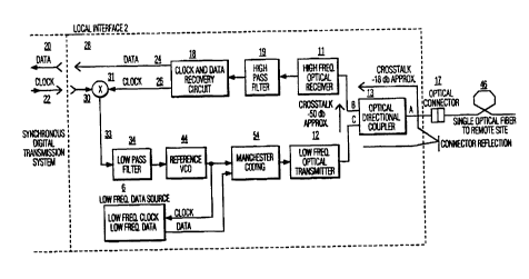
With reference to Figure 1, a synchronous digital
transmission system according to the present invention is
shown comprising a local interface unit 2 electronically
coupled to a data input terminal 20 and a system clock output
terminal 22 of the local or principal system (not further
shown). Unit 2 serves to develop low speed reference clock
signals as described below and apply them to the remote
information source or station 4 through an optical
transmission medium and receive high speed data streams and
apply them to the data input 20 of the local system.
Remote station 4 , according to the invention,
functions to receive the low speed reference clock signals,
use them to generate a high speed clock signal and use the
same to control the generation and transmission of high speed
W094/24790 PCT~S94/04244
0~
data streams back to the interface unit 2.
Communication is provided between interface unit 2 and
remote station 4 through optical connectors 17 and 47 and a
single optical fiber 46 that operates in a diplex mode in an
exemplary manner described below.
It will be understood that only one remote station 4 is
shown in the figure for simplicity, however, a plurality of
remote stations may be provided each communicating with
the local system over separate fiber links with a local
interface unit 2. It will also be understood that the delay
path in both directions provided by fiber 46 is variable by
as much as several bits of a high bit rate because of
temperature variations as described above.
Local interface unit 2 comprises an optical
directional coupler 13 having an input A coupled to receive
optical signals from connector 17, an input C coupled to
receive optical signals from low frequency optical
transmitter 12 and output B coupled to feed high speed data
signals to high frequency optical receiver 11.
Receiver 11 converts the optical digital
signals to electronic signals and applies them to high pass
filter 19 which filters out any low frequency signal
components appearing through crosstalk or reflection paths at
W094/24790 PCT~S94/04244
216~7~
receiver 11. A clock and data recovery circuit 18 separates
these electronic signals, the high speed data signals
appearing on lead 24 and port 28 and high speed clock signals
appearing on lead 26.
A phase detector 31, low pass filter 34 and reference
voltage controlled oscillator 44 (VCO) form a conventional
phase-locked loop circuit. Accordingly, any phase error
between the principal reference clock signals on
lead 30 compared to the high speed clock signals on lead 26,
will produce a voltage control signal on lead 33 that is
proportional to such phase error. The phase of the reference
VCO low frequency signal is controlled or adjusted in
response to this phase error and reduces this error to zero
as further described below.
The low speed reference clock signals are then applied
to a coding circuit 54 having the capability of shaping the
signal power-frequency spectrum so that the energy content of
signals outside a narrow band near the low and high speed
clock signal frequencies falls off rapidly. One such suitable
coding circuit includes a Manchester coding circuit which has
a spectral shape indicated in Figure 2. The line coded
reference clock signals are then converted to optical signals
by low frequency optical transmitter and applied to the
W094/24790 PCT~S94/04244
216~7~`~
coupler 13.
The remote unit 4 includes a low speed optical receiver
15 coupled to receive the low speed optical signals from
optical directional coupler 14 and to develop electronic low
speed clock signals at the same rate as the reference VCO
clock signals mentioned above. These reference clock signals
are used to control the phase of the high frequency VCO 42
clock signals that runs at the same frequency as the high
speed principal clock of the local system and that applies
its output signals to the remote data generator 40 to control
the timing of the remote information bit stream generation.
The phase of high speed clock signal VCO 42 output
signals is controlled in the following manner. Phase detector
32, low pass filter 36, high frequency VCO and frequency
divider form a phase - locked loop circuit. Phase detector 32
senses the reference clock signal from receiver 15 and
recovery circuit 25 and the output from frequency divider 38
that produces the same clock signal frequency as the
reference signal but at the phase produced by VCO 42. The
output from detector 32 represents the phase error between
its clock signal inputs. The phase error signal is fed to low
pass filter 36 and fed back to control the phase of the high
frequency clock signal VCO 42. Therefore the phase of the
W094/24790 PCT~S94/04244
~160770
output high speed data bit stream from unit 40 is controlled
by the phase of the reference clock signals that just arrived
from the variable delay path , namely fiber 46.
Both the high speed data and high frequency clock
signals are applied to leads 50 and 52 respectively and to a
high speed Manchester coding 49 circuit for power-frequency
spectral shaping (see Figure 2). Coded signals are then
applied to a high frequency optical transmitter 16 for
conversion to an optical signals bit stream and applied to
port B of optical directional coupler 14 for transmission
through variable delay path fiber 46 to local unit 2.
The harmful effects of using bidirection optical
digital transmission through a single fiber and using optical
couplers 13 and 14 in the system of figure 1 are avoided or
minimized by selecting non-standard line coding schemes for
the operating ranges of the information data bit rate and
the various low and high speed clock frequencies. These
codes should have the characteristics of having low energy
components in areas outside their designed frequency of
primary operation for reasons given above.
Figure 2 depicts one such useable optical line coding
scheme, namely, the use of Manchester codes for the low and
high clock frequencies. Note the power or energy content of
11
W094t24790 PCT~S94/04244
~ GO~ ~
the respective signals are low away from the respective
clock frequency or designed information bit rate and
therefore can be easily filtered out or otherwise have
little effect on the signal to noise ratio or information
degradation. For example, the effects of high frequency
crosstalk or reflections appearing at receiver 15 of unit 4
may be ignored because of their low energy content and the
frequency spectrum of the low frequency signals processed
through the recovery circuit 25.
In the event it is desired to generate a data bit stream
at the local or interface unit 2 for transmission to and use
by the remote unit (such as sending camera control
information to a remote video camera) , a low speed data
source 6 can be provided that generates data under control of
the reference VCO. The low speed data bits are coded by the
coding circuit 54 and become part of the optical signals
emitted by transmitter 12. Reference clock and low speed data
signals are separated by recovery circuit 25 with the low
speed data applied to destination circuit 5 that is also
controlled by reference clock signals from circuit 25.
In one example of the present embodiment , the highspeed
data rate is 200Mbit per second with a principal
frequency and high frequency clock signals of 200MHz and the
12
W094/24790 PCT~S94/04244
2l~a770
reference frequency clock signals at lOMHz. If the low speed
channel is used, the bit rate is lOMBits per second.
It will be appreciated that various modifications can be
made to the system and method of the embodiments disclosed
herein and that the inventive concepts hereof can be applied
in a great variety of synchronous digital optical systems
without departing from the spirit and scope of the present
invention.