Note: Descriptions are shown in the official language in which they were submitted.
2160829
P12906
-- 1 --
BACKGROUND OF THE INVENTION
1. Field of the Invention:
The present invention relates to an electronic
component and a method for fabricating the same. More
specifically, the present invention relates to an elec-
tronic component which includes a very rigid and solid
protection layer made of a metal oxide, so that an
element covered with the protection layer is effectively
sealed (i.e., having excellent moisture resistance and
chemical resistance, for example) and insulated, and the
resultant electronic component has excellent mechanical
strength and can be smoothly mounted, and a method for
fabricating the same.
2. Description of the Related Art:
Conventionally, an element of an electronic
component is covered with a protection layer in order to
protect the element from damage (for example, breaking,
cracking, and being strained) and deterioration (due to
moisture, gas, acid, alkali, and the like). For example,
Japanese Laid-Open Patent Publication No. 5-47513 and
No. 6-96907 disclose a multilayer varistor having a glass
protection layer. Japanese Laid-Open Patent Publication
No. 6-124807 discloses a multilayer varistor having
layers made of Fe203 or glass formed at the top and bottom
of the varistor. A resin protection layer made of a
thermosetting resin and the like is also known.
A glass protection layer tends to be peeled off
or cracked by shock and heat, and consequently allows
water to enter inside through the peeled or cracked por-
tion. The resin protection layer, which is hygroscopic
216082!~
- 2 - P12906
itself, does not sufficiently work as a protection layer
because a protection layer must shut off the inside from
an external environment. The protection layers formed at
the top and bottom of the varistor as disclosed in
Japanese Laid-Open Patent Publication No. 6-124807 do not
cover the entire surface of an element of the varistor,
and thus, do not provide sufficient sealing. According-
ly, conventional protection layers fail to provide suffi-
cient sealing (i.e., moisture resistance and chemical
resistance, for example) and insulation to an element
covered with the protection layer.
Further, the glass protection layer tends to be
peeled off and crack as described above. Accordingly,
the resultant electronic component having a glass protec-
tion layer is poor in mechanical strength and cannot be
smoothly mounted.
Thus, an electronic component capable of provid-
ing excellent sealing and insulation of an element
thereof as well as excellent mechanical strength and
smooth mounting is desired.
SUMMARY OF THE INVENTION
The electronic component of this invention
includes: an element having an internal electrode there-
in; an external electrode formed on an end portion of the
element where an end face of the internal electrode is
exposed; and a protection layer formed on the entire
surface of the element except for the end portion of the
element, wherein the protection layer is made of a metal
oxide.
2160~29
P12906
-- 3 --
In one embodiment of the invention, the electron-
ic component further includes a glass layer formed on the
surface of the protection layer.
In another embodiment of the invention, the metal
oxide contains a vitreous substance.
Alternatively, the electronic component includes:
an element; electrodes formed on a top surface and a
bottom surface of the element; and a protection layer
formed on the entire surface of the element except for
portions where the electrodes have been formed, wherein
the protection layer is made of a metal oxide.
According to another aspect of the invention, a
method for fabricating an electronic component is provid-
ed. The method includes the steps of: forming an exter-
nal electrode on an end portion of an element having an
internal electrode therein where the internal electrode
is exposed; forming a metal coat layer on the entire
surface of the element except for a portion where the
external electrode has been formed; and heat-treating the
element with the external electrode and the metal coat
layer formed thereon so as to oxidize the metal coat
layer on the element and thus to form a protection layer
made of a metal oxide.
In one embodiment of the invention, the method
further includes the step of forming a metal plating
layer on the external electrode.
In another embodiment of the invention, the
method further includes the step of dipping the element
2160~2~
P12906
in an alkaline solution of hydrogen peroxide after the
step of forming a metal plating layer, so as to re-
oxidize the protection layer.
In still another embodiment of the invention, the
metal coat layer is formed by electroless metal plating.
In still another embodiment of the invention, the
electroless metal plating is conducted using one of Ni
and Cu as a major component.
In still another embodiment of the invention,
powders containing at least one selected from the group
consisting of compounds containing Si, Ti, Al, Mg, and Zr
which form oxides by heat treatment are dispersed in a
metal plating solution used for the electroless metal
plating.
In still another embodiment of the invention,
glass powders are dispersed in a metal plating solution
used for the electroless metal plating.
Alternatively, the method for fabricating an
electronic component includes the steps of: dipping an
element having an external electrode on a portion of a
surface of the element and a protection layer made of a
metal oxide on the other portion of the element where the
external electrode has not been formed in a solution
containing a glass formation substance; and forming a
glass layer by heat-treating the element removed from the
solution.
In one embodiment of the invention, the method
2160829
P12906
further includes the step of forming a resist on the
external electrode before the step of dipping the element
in a solution containing a glass formation substance,
wherein the resist is carbonized simultaneously with the
formation of the glass layer by heat-treating the element
removed from the solution after the step of dipping the
element, and is removed from the surface of the external
electrode.
In another embodiment of the invention, the
resist is a paste.
In still another embodiment of the invention, the
solution includes at least one selected from the group
consisting of silica compounds represented by Si(OR1)4 and
R2mSi(OH)4m; titanium compounds represented by Ti(oR3)4 and
R4nTi(oH)4n; and aluminum compounds represented by Al(OR5)3
and R5qAl(OH)3q(wherein R1 to R5 individually denote alkyl
groups having 1 to 3 carbon atom(s), m and n are individ-
ually O to 4, and q is O to 3), an additive containing avitrifying agent and an organic binder, and an organic
solvent.
In still another embodiment of the invention, a
filler containing at least one selected form the group
consisting of needle-like crystals of Al203, TiO2, ZnO,
SiC, Si3N4, and SiO2, carbon fibers, and glass fibers is
dispersed in the solution.
In still another embodiment of the invention, a
second filler containing at least one compound selected
from the group consisting of Bi203 and Sb203 is dispersed
in the solution.
2160829
- 6 - P12906
In still another embodiment of the invention, the
step of forming a glass layer is conducted by heating the
element by putting the surface of the element in contact
with powders containing at least one selected from the
group consisting of compounds containing Si, Ti, Al, Mg,
and Zr which form oxides by heat treatment.
Alternatively, the method for fabricating an
electronic component includes the steps of: dipping an
element having an external electrode on a portion of a
surface of the element and a protection layer made of a
metal oxide on the other portion of the element where the
external electrode has not been formed in a solution
containing a resin component; and hardening the resin
component by heating the element removed from the solu-
tion.
Alternatively, the method for fabricating an
electronic component includes the steps of: dipping an
element having a protection layer made of a metal oxide
formed on the entire surface of the element except for an
end portion and an external electrode covering the end
portion and a portion of the protection layer in a solu-
tion containing a glass formation substance; and forming
a glass layer by heat-treating the element removed from
the solution.
Alternatively, the method for fabricating an
electronic component includes the steps of: dipping an
element having a protection layer made of a metal oxide
formed on the entire surface thereof except for an end
portion and an external electrode on the end portion and
a portion of the protection layer in a solution contain-
216Q82~
P12906
ing a resin component; and hardening the resin componentby heating the element removed from the solution.
In one embodiment of the invention, the resin
component is selected from silicone resins and epoxy
resins.
Thus, the invention described herein makes
possible the advantages of (1) providing an electronic
component where the sealing of an element thereof is
significantly high, ensuring the protection of the
element from water, gas, acid, alkali, and the like, and
thus excellent moisture resistance and chemical resis-
tance can be provided; (2) providing an electronic
component where the insulation of an element thereof is
significantly high and thus surface leakage and migration
at an external electrode are effectively reduced; (3)
providing an electronic component which has excellent
mechanical strength and shock resistance and thus can be
smoothly mounted; and (4) providing a method for fabri-
cating such electronic components.
These and other advantages of the present inven-
tion will become apparent to those skilled in the art
upon reading and understanding the following detailed
description with reference to the accompanying figures.
BRIEF DESCRIPTION OF THE DRAWINGS
Figure 1 is a schematic sectional view showing an
example of an electronic component according to the
present invention.
216082~
- 8 - P12906
Figure 2 is a schematic sectional view showing an
alternative example of the electronic component of Fig-
ure 1.
Figure 3 is a schematic sectional view showing
another example of an electronic component according to
the present invention.
Figure 4 is a schematic sectional view showing an
alternative example of the electronic component of Fig-
ure 3.
Figure 5 is a schematic sectional view showing
still another example of an electronic component accord-
ing to the present invention.
Figure 6 is a flowchart showing an example of the
method for fabricating an electronic component according
to the present invention.
Figure 7 is a flowchart showing a fabrication
method of Example 1.
Figure 8 is a flowchart showing a fabrication
method of Example 2.
Figure 9 is a flowchart showing a fabrication
method of Example 3.
Figure 10 is a flowchart showing a fabrication
method of Example 4.
Figure 11 is a flowchart showing a fabrication
216082~
P12906
method of Example 5.
Figure 12 is a flowchart showing a fabrication
method of Example 6.
Figure 13 is a schematic sectional view showing
an electronic component of a comparative example.
Figure 14 is a flowchart showing a fabrication
method of the electronic component of Figure 13.
Figure 15 is a schematic sectional view showing
an electronic component of another comparative example.
15Figure 16 is a flowchart showing a fabrication
method of the electronic component of Figure 15.
DESCRIPTION OF THE PREFERRED EMBODIMENTS
20Referring to Figure 1, a multilayer varistor will
be described as a preferred embodiment of an electronic
component according to the present invention.
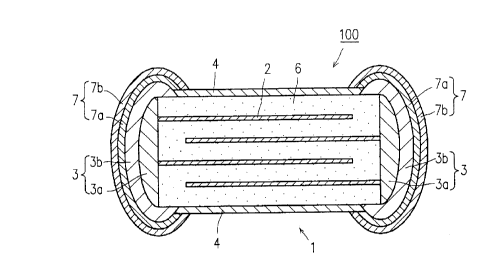
A multilayer varistor 100 includes: an element 1
25of a rectangular parallelepiped shape having internal
electrodes 2 formed therein; external electrodes 3 having
inner layers 3a formed on the both end faces of the
element 1 where end faces of the internal electrodes 2
are exposed and outer layers 3b formed so as to cover the
30inner layers 3a and the end portions of the four side
walls of the element 1; and protection layers 4 covering
the entire surface of the element 1 except for the por-
tions thereof where the external electrodes 3 are formed.
2160829
P12906
- 10 ~
The element 1 is formed by burning a multilayer
structure consisting of ceramic layers 6 and the internal
electrodes 2 alternately stacked at the same time. Only
one end face of each of the internal electrodes 2 reaches
one of the end faces of the element 1, and these end
faces of the internal electrodes 2 expose at the right or
left end faces of the element 1 alternately. These
exposed end faces of the internal electrodes 2 are
electrically connected with the inner layers 3a of the
external electrodes 3.
The ceramic layers 6 of the element 1 are made of
SrTiO3 as a major ingredient. The content of such a major
ingredient in a mixture forming the ceramic layers is
preferably 95% or more, more preferably 97% or more. As
minor ingredients of the mixture, Nb20s, Ta2O5, SiO2, MnO2,
Sb203, Bi2O3, Co2O3, CuO and the like may be used.
The internal electrodes 2 may be made of any
known electrode materials. For example, a mixture
containing Ni and the like as a major ingredient and
Li2C03, Na2CO3 and the like as a minor ingredient may be
used. Among them, a mixture containing Ni as a major
ingredient and Li2CO3 as a minor ingredient is preferably
used.
The inner layers 3a of the external electrodes 3
may be made of any known electrode material. For exam-
ple, Ni, Cu and the like are known. Among them, a
mixture containing Ni as a major ingredient and Li2CO3 as
a minor ingredient is preferably used. The thickness of
the thickest portion of the inner layers 3a is preferably
in the range of 10 to 15 ,um. The outer layers 3b of the
216082~
P12906
-- 11 --
external electrodes 3 are made of materials such as Ag
and Ag-Pd, for example. Among them, Ag is preferable.
The thickness of the thickest portion of the outer
layers 3b is preferably in the range of 30 to 60 ,um.
This two-layer structure of the external electrodes 3
provides an advantage in that reliability of the re-
sultant electronic component can be improved.
The protection layer 4 is made of a metal oxide.
Materials forming the metal oxide include: a metal such
as Ni, Cu; and metal compounds (such as Ni compound, Cu
compound) containing at least one oxide of Si, Ti, Al,
Mg, and Zr. Among these materials, Ni and Ni compound
containing at least one oxide of Si, Ti, Al, Mg, and Zr
are preferable because the oxide thereof has an especial-
ly high resistance value and good chemical resistance.
By having the protection layer made of a metal oxide, the
element is effectively sealed (i.e., having excellent
moisture resistance and chemical resistance, for example)
and insulated. The resultant electronic component is
provided with excellent mechanical strength and can be
smoothly mounted.
The metal oxide preferably includes a vitreous
substance such as lead glass. The content of the vitre-
ous substance is preferably in the range of 1 to 10 g,
more preferably in the range of 3 to 6 g for 100 ml of
electroless metal plating solution.
The thickness of the protection layer 4 is
preferably in the range of about 0.5 to about 5 lum, more
preferably in the range of about 1 to about 3 ~m. When
the thickness of the protection layer 4 is less than
2160829
- 12 - P12906
about 0.5 ,um, the uniformity of the thickness is not
obtainable, and a hole may be generated in the protection
layer 4. As a result, the moisture resistance of the
resultant multilayer varistor may be insufficient. On
the contrary, when the thickness of the protection
layer 4 is more than about 5 ,um, the element may break or
crack due to a volumetric change of the metal of the
protection layer 4 at the time of the oxidation of the
metal. Further, re-oxidation of the metal oxide tends to
become difficult.
Preferably, as shown in Figure 2, the multilayer
varistor 100 may further include a glass layer 5 formed
on the surface of the protection layer 4 and/or metal
plating layers 7 covering the external electrodes 3. The
glass layer 5 preferably includes a glass formation sub-
stance and a vitrifying agent. Examples of the glass
formation substance include: silica compounds represented
by Si(OR1)4 and R2mSi(OH)4m; titanium compounds represented
by Ti(oR3)4 and R4nTi(oH)4n; aluminum compounds represented
by Al(OR5)3 and R6qAl(OH)3q; and mixtures thereof (wherein
R1 to R6 individually denote alkyl groups having 1 to 3
carbon atom(s), m and n are individually 0 to 4, and q is
0 to 3). Examples of the vitrifying agent include oxides
of Na, Li, K, Bi, B, and Pb. By forming such a specific
glass layer, the sealing of the element is further
enhanced. In the case where the metal plating layers are
formed over the external electrodes 3, portions of the
protection layer may be reduced due to hydrogen gas
generated at the formation of the metal plating layers.
The formation of the glass layer prevents reduction of
the protection layer due to hydrogen gas.
21~0~2g
P12906
- 13 -
The thickness of the glass layer 5 is preferablyin the range of about 1 to about 3 ,um, more preferably in
the range of about 1.5 to about 2.5 ,um. When the thick-
ness of the glass layer 5 is less than about 1 ,um, the
uniformity of the thickness is not obtainable, and a hole
or a scratch may be easily generated in the glass lay-
er 5. As a result, the moisture resistance of the
resultant multilayer varistor may be insufficient. On
the contrary, when the thickness of the glass layer 5 is
more than about 3 ,um, the glass layer 5 may be peeled off
or crack due to heat and/or shock.
Preferably, the glass layer 5 may contain a
filler. Examples of the filler include: needle-like
crystals of Al2O3, TiO2, ZnO, SiC, Si3N4, and SiO2; carbon
fibers; and glass fibers. The crystals or fibers of the
filler are preferably shaped as fine as possible.
Specifically, they preferably have a length of about
5.0 ,um or less and a diameter of about 1.0 ,um or less.
The size distribution of the filler is desirably as small
as possible. The content of the filler may be preferably
in the range of 0.1 to 5.0 parts by weight, more prefera-
bly in the range of 0.5 to 2.0 parts by weight for 100
parts by weight of the glass formation substance. By
having such needle-like filler in the glass layer, both
the thermal strength and mechanical strength of the glass
layer are enhanced, thereby suppressing cracking and
peeling off of the glass layer. The resultant electronic
component can be smoothly mounted. Further, the bond
strength between the protection layer and the glass layer
eminently increases by the anchoring effect of the
filler. The resultant electronic components provides
excellent moisture resistance.
2160829
P12906
- 14 -
Preferably, the glass layer 5 may further containa second filler containing at least one compound selected
from Bi203 and Sb203. The content of the second filler may
be preferably in the range of 0.1 to 5.0 parts by weight,
more preferably in the range of 0.2 to 2.0 parts by
weight for 100 parts by weight of the glass formation
substance. The bond strength between the protection
layer and the glass layer is eminently increased by the
diffusion effect of the second filler in the glass layer.
Each of the metal plating layers 7 preferably has
a two-layer structure composed of an inner metal plating
layer 7a and an outer metal plating layer 7b. The inner
metal plating layer 7a is made of Ni, Cu, and the like.
Among them, Ni is preferable. The outer metal plating
layer 7b is made of a solder, Sn, and the like. Among
them, a solder is preferable. By covering the external
electrodes 3 with the metal plating layers 7, the resul-
tant multilayer varistor can be smoothly mounted.
Alternatively, the multilayer varistor 100 may
include a resin layer, instead of the glass layer, on the
protection layer 4, though this structure is not shown.
Examples of the resin forming the resin layer include
thermosetting resins such as silicone resins and epoxy
resins. The thickness of the resin layer is preferably
in the range of about 1 to about 3 ,um, more preferably in
the range of about 1.5 to about 2.5 ,um, as in the case of
the glass layer. By forming such a resin layer, the
sealing of the element is further enhanced. In the case
where the metal plating layers are formed over the exter-
nal electrodes 3, portions of the protection layer may be
reduced due to hydrogen gas generated at the formation of
2160829
P12906
- 15 -
the metal plating layers. The formation of the resinlayer prevents reduction of the protection layer due to
hydrogen gas.
Figure 3 shows another example of the multilayer
varistor according to the present invention. A
multilayer varistor 100 of this example includes: an
element 1 of a rectangular parallelepiped shape having
internal electrodes 2 formed therein; protection layers 4
covering the entire surface of the element 1 except for
both end faces thereof; and external electrodes 3 having
inner layers 3a formed on the end faces of the element 1
and outer layers 3b formed so as to cover the inner lay-
ers 3a and the end portions of the protection layer 4.
The multilayer varistor of this example, as in the
multilayer varistor shown in Figure 1, may further
include a glass layer 5 and/or metal plating layers 7 as
shown in Figure 4.
Figure 5 shows a disk-shaped thermistor as
another preferred embodiment of the electronic component
of the present invention. Only components specific to
the thermistor are described herein for simplification.
Referring to Figure 5, a thermistor 500 includes
a disk-shaped element 1, electrodes 2 formed on the top
and bottom surfaces of the element 1, and protection
layers 4 formed on the entire surface of the element 1
except for the portions thereof where the electrodes 2
are formed.
Any known thermistor element may be used for the
element 1. Typically, an element made of a composite
2160829
- 16 - P12906
material of Mn-Ni-Cu, Mn-Ni-Fe, Mn-Ni-Al, or the like is
used.
Any known thermistor electrode may be used for
the electrodes 2. Typically, an electrode made of Ag,
Ag-Pd, or the like is used.
The electronic components of specific shapes and
usages were described hereinbefore for simplification.
However, the present invention can be applied to any
shapes of elements and used for various types of elec-
tronic components other than those described above. For
example, the present invention is also applicable to
capacitors, multilayered thermistors, ceramistors,
varistors, ferrites, ceramic substrates, and piezoelec-
tric elements, in addition to the multilayer varistors
and the disk-shaped thermistors as described above.
Furthermore, the present invention is applicable to any
shapes of electronic components (for example, multilay-
ered type, disk-shaped type).
Next, a preferred example of the method for
fabricating an electronic component according to the
present invention will be described with reference to the
flowchart of Figure 6.
First, the element is prepared by a known method.
The fabrication of the element is not a constituent of
the present invention, but any known fabrication method
may be adopted. For example, in the case of the
multilayer varistor shown in Figure 1, the element is
fabricated in the following manner (steps (A) and (B)).
2160829
P12906
- 17 -
A ceramic sheet is first fabricated in thefollowing procedure (step (A)): The above-mentioned
ceramic materials for the ceramic layers are mixed at a
predetermined ratio. The mixture is calcined and then
ground into powders. The average diameter of the powders
is preferably 1.0 ,um or less, more preferably 0.6 to
0.8 ,um. The resultant powders are mixed with an organic
binder and an organic solvent so as to form a slurry.
Examples of the organic binder include butyral resins,
cellulose resins, and the like. Examples of the organic
solvent include butyl acetate, dibutyl phthalate (DBP)
and the like. The resultant slurry is formed into a
sheet by a known method such as a doctor-blade method and
a reverse-rolls method, and the sheet is then cut to form
ceramic sheets for the ceramic layers. The thickness of
each ceramic sheet is preferably in the range of 20 to
50 ,um, more preferably in the range of 25 to 30 ,um.
Then, the element is fabricated in the following
procedure (step (B)): A conductive paste is prepared
from the above-mentioned internal electrode formation
materials. Using the paste, the internal electrodes of
a desired shape are formed on the ceramic sheets by
screen printing, gravure printing, or the like. In the
case of the multilayer varistor shown in Figure 1, while
one end face of each internal electrode extends to one
end face of the ceramic sheet, the other end face thereof
does not reach the other end face of the ceramic sheet
but is located between the ends of the ceramic sheet.
Such ceramic sheets and the internal electrodes are
stacked alternately until a predetermined number of
layers are stacked in such a manner that the end faces of
the internal electrodes extend to the right or left end
21608Z9
P12906
- 18 -
faces of the ceramic sheets alternately. Each of the topand bottom surfaces of the thus-obtained multilayer
structure is covered with a dummy ceramic sheet. The
resultant structure is heated, pressed, and cut into a
predetermined shape. The multilayer structure cut into
the predetermined shape is decarbonized, calcined and
chamfered. The organic binder and the organic solvent
are removed at the decarbonization and calcination.
Thus, production of the element is completed. The calci-
nation is conducted at a temperature preferably in therange of 1000 to 1200C, more preferably in the range of
1000 to 1100C for preferably 1 to 5 hours, more prefera-
bly 1 to 2 hours. The heating rate is preferably in the
range of 10 to 50C/hour.
Thereafter, a paste for the formation of the
external electrodes is applied to the end faces of the
thus-obtained element to a predetermined thickness (step
(C)), and then burned for reduction (step (D)). This
burning is conducted at a temperature preferably in the
range of 1200 to 1300C, more preferably in the range of
1200 to 1250C for preferably 1 to 10 hours, preferably
2 to 5 hours. The heating rate is preferably about
200C/hour.
Then, a metal coat layer is formed on the entire
surface of the element except for the portions thereof
where the external electrodes are formed to a predeter-
mined thickness (step (E)). The metal coat layer, which
is to be the protection layer by heat treatment, may be
formed by electroless metal plating, vapor deposition,
sputtering, dipping, thermal spraying, printing, and the
like. Among these methods, electroless metal plating is
2160829
P12906
- 19 -
preferable, and an electroless metal plating using eitherNi or Cu as a major component is more preferable. The
dip of the element into a metal plating solution should
preferably be conducted after the surface of the element
is sufficiently cleaned with pure water or ion exchange
water for the removal of impurities. The metal plating
solution preferably contains glass powders or powders
including at least one material selected from the group
consisting of compounds of Si, Ti, Al, Mg, and Zr which
form oxides by heat treatment. Such powders are prefera-
bly uniformly dispersed in the metal plating solution.
For the uniform dispersion of the powders, the metal
plating solution should be agitated vigorously while the
powders are added thereto. The content of the powders is
preferably in the range of 1 to 10 g, more preferably in
the range of 3 to 6 g for 100 ml of the metal plating
solution. The existence of the powders in the metal
plating solution ensures the formation of the protection
layer having high reduction resistance or high mechanical
strength.
The metal coat layer is selectively formed on the
surface of the element except for the external electrode
formation portions by using resists, masking, and the
like. Among these methods, using resists is preferable.
Such resists may be made of pastes of polysaccharides
such as ethyl cellulose, resins such as polyvinyl alcohol
and polyvinyl acetate, and the like. Among them, pastes
are preferable. The resists are preferably colored with
a dye or a pigment so that the uniformity of the resul-
tant resists can be easily observed. The resists are
carbonized by heating at the formation of the protection
layer to be described later, and thus can be easily
2160829
P12906
- 20 -
removed. The carbonized resists are removed by ultrason-
ic cleaning and barrel polishing, for example.
In the case where the two-layer external elec-
trodes are to be formed, the inner and outer layers of
the external electrodes and the metal coat layer are
formed in the following procedure: (i) A paste for the
formation of the inner layers of the external electrodes
is applied to the end faces of the element obtained at
step (B) to a predetermined thickness, and then burned
for reduction; (ii) A paste for the formation of the
outer layers of the external electrodes is applied to a
predetermined thickness; and (iii) the metal coat layer,
which is to be the protection layer by heat treatment, is
formed on the entire surface of the element except for
the portions where the external electrodes have been
formed. Alternatively, the metal coat layer may be
formed on the entire surface of the element except for
the portions where the inner layers of the external elec-
trodes have been formed after step (i), followed by the
formation of the outer layers of the external electrodes.
Subsequently, the metal coat layer is oxidized by
heat treatment so as to form the protection layer made of
an metal oxide (step (F)). The heat treatment is con-
ducted at a temperature preferably in the range of 700 to
850C, more preferably in the range of 750 to 850C for
preferably lO minutes to 2 hours, more preferably 30
minutes to 1 hour.
Preferably, the metal plating layers are formed
on the element after the formation of the protection
layer (step (G)). Further, the protection layer is
2160829
P12906
- 21 -
preferably re-oxidized after the formation of the metal
plating layers (step (G')). The re-oxidation is conduct-
ed, for example, by dipping the element with the protec-
tion layer formed thereon in an alkaline solution of
hydrogen peroxide or any other alkaline solution that
does not affect the element. An example of the alkaline
solution of hydrogen peroxide is a mixed solution of 30
hydrogen peroxide solution and 28~ aqueous ammonia solu-
tion in the volume ratio of 10:1. The duration of dip is
preferably 1 to 10 minutes, more preferably 1 to 2
minutes. By this re-oxidation, the reduction resistance
of the protection layer is further enhanced. Since the
solution used for the re-oxidation has a cleaning effect,
it can also be used as the cleaning solution after the
metal plating.
After the re-oxidation, the resultant structure
is preferably chamfered. Even if the protection layer is
undesirably formed on the outer layers of the external
electrodes, the portions of the protection layer formed
on the outer layers of the external electrodes can be
selectively removed by chamfering. Thus, an electronic
component where the protection layer is formed only on a
desired portion can be obtained. For example, for the
outer layers made of Ag, since the ductility of Ag is
high, the coefficient of friction between the outer
layers of the external electrodes and the protection
layer is large. This facilitates the grinding of the
portions of the protection layer on the outer layers at
the chamfering. As a result, only the portions of the
protection layer on the outer layers can be effectively
removed.
216~8~
P12906
- 22 -
Preferably, the glass layer may be formed on the
surface of the protection layer formed on the surface of
the element. Resists and the like may be used for the
selective formation of the glass layer on the surface of
5the protection layer formed on the surface of the ele-
ment, as in the case of the formation of the protection
layer. The glass layer may be formed by dipping, thermal
spraying, printing, and the like. In the dipping, for
example, the element with the protection layer formed
10thereon is dipped in a solution containing the above-
mentioned glass formation substance and then heat-treat-
ed. One representative example of such a dipping solu-
tion is an alkoxide glass solution. The dipping of the
element into the solution should preferably be conducted
15after the surface of the element has been sufficiently
cleaned with pure water or ion exchange water for the
removal of impurities. The water used for the cleaning
should preferably be removed completely before the
dipping of the element so as to prevent the solution from
20being hydrolyzed. The duration of dipping is preferably
in the range of 1 to 10 minutes, more preferably in the
range of 2 to 5 minutes. After the dipping, drops of
solution attaching to the element may be removed by
centrifugation. Then, the heat treatment is conducted at
25a temperature preferably in the range of 200 to 500C,
more preferably in the range of 250 to 400C for prefera-
bly 10 minutes to 2 hours, more preferably 30 minutes to
l hour. The heat treatment is conducted preferably by
putting the surface of the element in contact with
30powders containing at least one material selected from
the group consisting of compounds containing Si, Ti, Al,
Mg, and Zr (for example, by burying the element among the
powders) so as to heat the element. The purity of the
21~08~
P12906
- 23 -
powders is preferably 90% or more, more preferably 95% ormore. This heating of the element by the contact with
the powders is effective in suppressing the diffusion
reaction between the protection layer and the glass layer
and preventing the attachment of the element with other
elements at the formation of the glass layer. The above
process of dipping and heating is repeated preferably 1
to 3 times, more preferably 2 to 3 times. By thus
repeating the dipping and heating process, a more uniform
glass layer can be formed. As a result, the sealing of
the element is further enhanced.
Alternatively, the resin layer, instead of the
glass layer, may be formed on the protection layer formed
on the surface of the element. The resin layer is
formed, for example, by dipping the element with the
protection layer formed thereon in a solution containing
a resin component and then heat-treating so as to harden
the resin component. A representative example of the
immersion solution is a solution containing 100 parts by
weight of a resin component and 200 parts by weight of an
organic solvent. The duration of dipping is preferably
in the range of 5 to 30 minutes, more preferably in the
range of 5 to 10 minutes. The heat treatment is con-
ducted at a temperature preferably in the range of 100 to350C, more preferably in the range of 150 to 300C for
preferably 10 minutes to 2 hours, more preferably 10 to
30 minutes.
According to the present invention, an electronic
component having a protection film made of a metal oxide
is obtained. The protection layer is very rigid and
solid because the volume of the metal oxide increases at
21Sû82~
P12906
- 24 -
the formation thereof by the oxidation of a metal.
Further, the protection layer bonds to the surface of the
element not only physically but also by chemical reaction
between a portion of the protection layer and the surface
portion of the element. As a result, the electronic
component of the present invention has the following
features: (I) The sealing of the element is significantly
high, ensuring the protection thereof from water, gas,
acid, alkali, and the like. Accordingly, even if the
element itself is porous, high moisture resistance and
chemical resistance can be obtained. (II) The insulation
of the element is significantly high, and thus surface
leak and migration at the external electrode are effec-
tively reduced. (III) The resultant electronic component
has significantly excellent mechanical strength and shock
resistance. As a result, occurrence of damages such as
breaks and cracks and strains is prevented. (IV) The
resultant electronic component can be smoothly mounted.
(V) The bond strength between the element and the protec-
tion layer is significantly high. Thus, the protection
layer is prevented from being peeled off and cracking due
to shock and heat.
(Examples)
The present invention is now specifically de-
scribed by way of examples though it is not limited to
these examples.
Example 1
A multilayer varistor as shown in Figure 1 was
fabricated according to the flowchart shown in Figure 7.
First, ceramic sheets for the ceramic layers were
2160829
P12906
- 25 -
formed in the following procedure: SrTiO3 (98.6 mol%),Nb20s (0.2 mol%), Ta205 (0.2 mol%), SiO2 (0.5 mol%), and
MnO2 (0.5 mol%) were mixed and ground in a ball mill for
20 hours, so as to obtain powders having an average
particle diameter of about 1.0 ,um or less. For 100 parts
by weight of the resultant powders, 10 parts by weight of
a butyral resin as the organic binder, 70 parts by weight
of butyl acetate as the organic solvent, and 5 parts by
weight of dibutyl phthalate (DBP) as the plasticizer were
mixed so as to form a slurry. The slurry was formed into
a sheet by the reverse-rolls method and cut, so as to
obtain the ceramic sheets having a thickness of about
30 um.
A conductive paste containing Ni as a major
component and Li2CO3 as a minor component was prepared.
The conductive paste was applied to the ceramic sheets by
screen printing so as to form the internal electrodes 2
on the ceramic sheets. Each of the internal electrodes 2
was printed so that one end face thereof extends to an
end face of the ceramic sheet, while the other end face
thereof does not reach the other end face of the ceramic
sheet but is located anywhere on the ceramic sheet. Such
ceramic sheets and the internal electrodes were stacked
alternately until a predetermined number of layers were
stacked in such a manner that the end faces of the
internal electrodes extend to the right or left end faces
of the ceramic sheets alternately. Each of the top and
bottom surfaces of the thus-obtained multilayer structure
was covered with a dummy ceramic sheet. The resultant
structure was heated, pressed, and cut into a predeter-
mined shape. The multilayer structure cut into the
predetermined shape was calcined at 1100C for 2 hours
216U8`~
P12906
- 26 -
and chamfered. The organic binder and the organicsolvent were removed at the calcination, Thus, the ele-
ment 1 was completed.
Thereafter, an Ni paste for the formation of the
inner layers 3a of the external electrodes was applied to
the end faces of the thus-obtained element 1, and the
element with the Ni paste was burned at 1250C for 5
hours for reduction. Then, an Ag paste for the formation
of the outer layers 3b of the external electrodes was
applied to the inner layers and the end portions of the
four walls of the element.
Resists made of a paste were formed on the thus-
obtained outer layers 3b of the external electrodes.
Then, a metal coat layer was formed on the entire surface
of the element except for the resist-formed portions to
a thickness of 1.0 ,um by electroless Ni plating. The
element with the metal coat layer formed thereon was then
heat-treated at 850C for 30 minutes, so as to form the
protection layer 4. The resists, which had been carbon-
ized at the heat treatment, were removed by ultrasonic
cleaning. Thereafter, the Ni inner plating layers 7a and
the solder outer plating layers 7b were formed on the
outer layers 3b of the external electrodes.
The multilayer varistor of Example 1 has a very
rigid and solid protection layer. This is formed because
the volume of the metal oxide increases at the formation
thereof by the oxidation of a metal. Further, the
protection layer bonds to the surface of the element not
only physically but also by chemical reaction between a
portion of the protection layer and the surface portion
21~08~
P12906
- 27 -
of the element. As a result, the electronic component ofExample 1 has the following features.
(I) The sealing of the element is significantly
high, ensuring the protection thereof from water, gas,
acid, alkali, and the like. Accordingly, the element is
excellent in moisture resistance and chemical resistance.
(II) The insulation of the element is signifi-
cantly high, and thus surface leakage and migration atthe external electrode are effectively reduced.
(III) The resultant electronic component has
significantly excellent mechanical strength and shock
resistance. As a result, occurrence of damage such as
breaks and cracks and strains is prevented.
(IV) The resultant electronic component can be
smoothly mounted.
(V) The bond strength between the element and the
protection layer is significantly high. Thus, the
protection layer is prevented from being peeled off and
cracking due to shock and heat.
Example 2
A multilayer varistor as shown in Figure 2 was
fabricated according to the flowchart shown in Figure 8.
Basically, the varistor was fabricated in the same manner
as that described in Example 1 except that a glass layer
was additionally formed.
Specifically, the element with the protection
2160829
P12906
- 28 -
layer 4 formed thereon was dipped in an alkoxide glass
solution (OCD series, manufactured by Tokyo Ohka Kogyo
Co. LTD.) for 5 minutes. The element was then removed
from the solution, and heated at 850C for 30 minutes by
putting the element in contact with powders containing
SiO2. Thus, the glass layer 5 was formed. The thus-
formed glass layer 5 not only bonds to the surface of the
protecting layer 4, but also partially intrudes into the
protection layer 4. Accordingly, the bond strength
between the protection layer 4 and the glass layer 5 is
significantly high.
Because the multilayer varistor of Example 2 has
the glass layer 5 formed on the protection layer 4, the
features (I) to (V) described in Example 1 were obtained
more effectively than in the case of Example 1. Espe-
cially, even when the multilayer varistor is immersed in
a gas or a solution with high reduction property, the
metal oxide constituting the protection layer is prevent-
ed from being reduced thanks to the covering of the glass
layer. Thus, the element can be further effectively
blocked from outside.
Example 3
A multilayer varistor as shown in Figure 1 was
fabricated according to the flowchart shown in Figure 9.
Basically, the varistor was fabricated in the same manner
as that described in Example 1 except that 5 g of Al2O3
powders were dispersed in 100 ml of an electroless metal
plating solution for the formation of the metal coat
layer.
As a result, in addition to the features (I) to
216118~
P12906
- 29 -
(V) described in Example 1, the resultant multilayer
varistor of Example 3 has the following feature: because
the protection layer 4 contains Al203 powders, it shows
excellent reduction resistance.
Example 4
A multilayer varistor as shown in Figure 3 was
fabricated according to the flowchart shown in Figure 10.
The element 1 was fabricated in the same manner
as that described in Example 1. An Ni paste for the
formation of the inner layers 3a of the external elec-
trodes was applied to the end faces of the element 1 and
then burned at 1250C for 5 hours for reduction. There-
after, resists made of a paste were formed on the inner
layers 3a of the external electrodes. Then, the metal
coat layer was formed on the entire surface of the
element except for the resist-formed portions to a
thickness of 1.0 ~m by electroless Ni plating. After the
resists were removed, an Ag paste for the formation of
the outer layers 3b of the external electrode was applied
to the surfaces of the inner layers 3a and portions of
the metal coat layer. The resultant element was heat-
treated at 850C for 30 minutes. Thus, the protection
layer 4 was formed. Thereafter, the Ni inner plating
layers 7a and the solder outer plating layers 7b were
formed on the outer layers 3b of the external electrodes.
The multilayer varistor of Example 4 has a very
rigid and solid protection layer. This is formed because
the volume of the metal oxide increases at the formation
thereof by the oxidation of a metal. Further, the
protection layer bonds to the surface of the element not
21608~
P12906
- 30 -
only physically but also by chemical reaction between a
portion of the protection layer and the surface portion
of the element. As a result, the multilayer varistor of
Example 4 has the following features.
(I) The sealing of the element is significantly
high, ensuring the protection thereof from water, gas,
acid, alkali, and the like. Accordingly, the element is
excellent in moisture resistance and chemical resistance.
(II) The insulation of the element is signifi-
cantly high, and thus surface leakage and migration at
the external electrode are effectively reduced.
(III) The resultant electronic component has
significantly excellent mechanical strength and shock
resistance. As a result, occurrence of damage such as
breaks and cracks and strains is prevented.
(IV) The resultant electronic component can be
smoothly mounted.
(V) The bond strength between the element and the
protection layer is significantly high. Thus, the
protection layer is prevented from being peeled off and
cracking due to shock and heat.
Further, in the multilayer varistor of Example 4,
the protection layer is formed on the entire surface of
the element except for the portions thereof where the
inner layers 3a of the external electrodes have been
formed. Accordingly, the following feature can be
additionally obtained.
216082~
P12906
- 31 -
(VI) Migration between the outer layers 3b of theexternal electrode and the internal electrodes 2 can be
significantly reduced.
Example 5
A multilayer varistor as shown in Figure 4 was
fabricated according to the flowchart shown in Figure 11.
Actually, the varistor was fabricated in the same manner
as that described in Example 4 except that the glass
layer was additionally formed.
Specifically, the element with the protection
layer 4 formed thereon was immersed in an alkoxide glass
solution (OCD series, manufactured by Tokyo Ohka Kogyo
Co. LTD.) for 5 minutes. The element was then removed
from the solution, and heated at 850C for 30 minutes by
putting the element in contact with powders containing
SiO2. Thus, the glass layer 5 was formed. The thus-
formed glass layer 5 not only bonds to the surface of the
protecting layer, but also partially intrudes into the
protection layer 4. Accordingly, the bond strength
between the protection layer 4 and the glass layer 5 is
significantly high.
Because the multilayer varistor of Example 5 has
the glass layer 5 formed on the protection layer 4, the
features (I) to (V) described in Example 4 were obtained
more effectively than in the case of Example 4. Espe-
cially, even when the multilayer varistor is immersed in
a gas or a solution with high reduction property, the
metal oxide constituting the protection layer is prevent-
ed from being reduced thanks to the covering of the glass
layer. Thus, the element can be further effectively
~160829
P12906
- 32 -
blocked from outside.
Example 6
A multilayer varistor as shown in Figure 3 was5 fabricated according to the flowchart shown in Figure 12.
Actually, the varistor was fabricated in the same manner
as that described in Example 4 except that 5 g of Al203
powders were dispersed in 100 ml of an electroless metal
plating solution for the formation of the metal coat
layer.
As a result, in addition to the features (I) to
(V) described in Example 4, the resultant multilayer
varistor of Example 6 has the following feature: because
the protection layer 4 contains Al203 powders, it shows
excellent reduction resistance.
Comparative example 1
A multilayer varistor as shown in Figure 13 was
fabricated according to the flowchart shown in Figure 14.
The varistor includes a metal coat layer formed on the
end faces and the end portions of the four walls of the
element.
The element 1 was formed in the same manner as
that described in Example 1. An Ni paste for the forma-
tion of the inner layers 3a of the external electrodes
was applied to the end faces of the element 1 and then
burned at 1250C for 5 hours for reduction. Thereafter,
a metal coat layer was formed on the entire surface of
the element with the inner layers 3a formed thereon to a
thickness of 1.0 ,um by electroless Ni plating. Then, an
Ag paste for the formation of the outer layers 3b of the
216082~
P12906
- 33 -
external electrodes was applied to the end faces of theelement and the end portions of the four walls of the
element, so as to partly cover the metal coat layer. The
resultant element was heat-treated at 850C for 30
minutes. As a result, only the portion of the metal coat
layer which had not been covered with the outer layers 3b
of the external electrodes was oxidized, forming the
protection layer 4. The remaining portions of the metal
coat layer covered with the outer layers 3b of the
external electrodes were hardly oxidized and remained as
the metal coat layers. Thereafter, the Ni inner plating
layers 7a and the solder outer plating layers 7b were
formed on the outer layers 3b of the external electrodes.
The varistor of Comparative example 1 has the
metal coat layers 8 remaining between the inner layers 3a
and the outer layers 3b of the external electrodes as
shown in Figure 13. Because the metal coat layers 8 bond
to the inner layers 3a and the outer layers 3b only
physically, the bond strength of the external electrodes
of the varistor of Comparative example 1 is low compared
with that of the external electrodes of the varistors of
Examples 1 to 6. As a result, the varistor of Compara-
tive example 1 is poor in surge resistance and pulse
resistance.
Comparative example 2
A multilayer varistor as shown in Figure 15 was
fabricated according to the flowchart shown in Figure 16.
Basically, the varistor was fabricated in the same manner
as that described in Comparative example 1 except that a
glass layer was additionally formed.
2160829
P12906
- 34 -
Specifically, the element with the protectionlayer 4 formed thereon was immersed in an alkoxide glass
solution (OCD series, manufactured by Tokyo Ohka Kogyo
Co. LTD.) for 5 minutes. The element was then removed
from the solution, and heated at 850C for 30 minutes by
putting the element in contact with powders containing
SiO2. Thus, the glass layer 5 was formed.
As in the multilayer varistor of Comparative
example 1, the multilayer varistor of Comparative exam-
ple 2 has the metal coat layers 8 remained between the
inner layers 3a and the outer layers 3b of the external
electrodes. Accordingly, the bond strength of the
external electrodes is low, and as a result, the varistor
of Comparative example 2 is poor in surge resistance and
pulse resistance.
Various other modifications will be apparent to
and can be readily made by those skilled in the art
without departing from the scope and spirit of this
invention. Accordingly, it is not intended that the
scope of the claims appended hereto be limited to the
description as set forth herein, but rather that the
claims be broadly construed.