Language selection

Search

Patent 2161170 Summary

Third-party information liability

Some of the information on this Web page has been provided by external sources. The Government of Canada is not responsible for the accuracy, reliability or currency of the information supplied by external sources. Users wishing to rely upon this information should consult directly with the source of the information. Content provided by external sources is not subject to official languages, privacy and accessibility requirements.

Claims and Abstract availability

Any discrepancies in the text and image of the Claims and Abstract are due to differing posting times. Text of the Claims and Abstract are posted:

  • At the time the application is open to public inspection;
  • At the time of issue of the patent (grant).
(12) Patent Application: (11) CA 2161170
(54) English Title: BATTERY FEED CIRCUIT
(54) French Title: CIRCUIT D'ALIMENTATION DE BATTERIES
Status: Deemed Abandoned and Beyond the Period of Reinstatement - Pending Response to Notice of Disregarded Communication
Bibliographic Data
(51) International Patent Classification (IPC):
  • H04M 19/00 (2006.01)
(72) Inventors :
  • SCHORR, IAN ANDREW (United States of America)
  • SPIRES, DEWAYNE ALAN (United States of America)
(73) Owners :
  • AT&T CORP.
(71) Applicants :
  • AT&T CORP. (United States of America)
(74) Agent: KIRBY EADES GALE BAKER
(74) Associate agent:
(45) Issued:
(22) Filed Date: 1995-10-24
(41) Open to Public Inspection: 1996-06-20
Examination requested: 1995-10-24
Availability of licence: N/A
Dedicated to the Public: N/A
(25) Language of filing: English

Patent Cooperation Treaty (PCT): No

(30) Application Priority Data:
Application No. Country/Territory Date
359,164 (United States of America) 1994-12-19

Abstracts

English Abstract


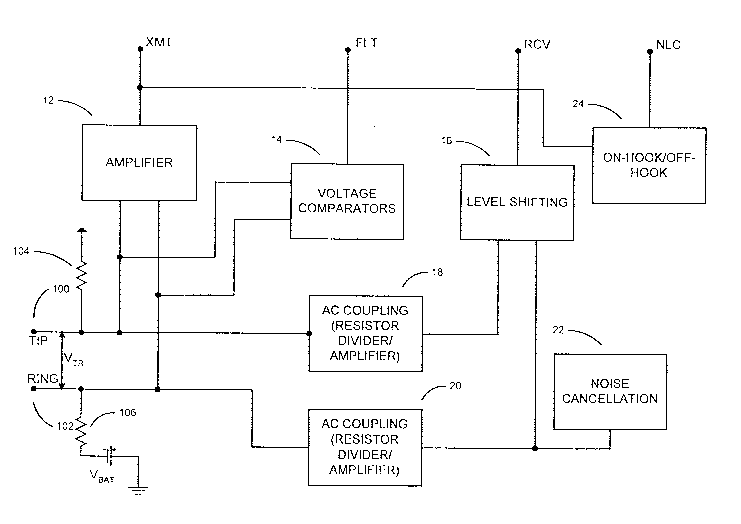
Resistive circuits are provided at the tip and ring of the battery feed circuit as
a method of alleviating the need for bulky DC transformers or complex integratedcircuitry. The voltage is monitored through a set of comparators eliminating theexpense of maintaining fused resistors. The voltages for voice or data transmission is
amplified prior to being transmitted. Received signals are AC coupled, with proper
biasing, onto the tip and ring lines. Any AC noise on the tip and ring line is shifted
180 degrees out of phase and re-inserted on the line to cancel the noise. As an
enhancement to the battery feed circuit, another voltage comparator is added to check
the line for DC current signifying an off hook condition.


Claims

Note: Claims are shown in the official language in which they were submitted.


- 5 -
CLAIMS:
1. A circuit for supplying direct current for a two-wire communication
transmission path comprising:
a resistive feed circuit supplying said direct current to said transmission
path,
tip and ring amplification means for sourcing and sinking current for
respective conductors of a telephone line,
an amplification circuit for transmitting said communication;
voltage protection means for guarding against an overvoltage condition;
and
an AC coupling network for receiving said communication.
2. The circuit of Claim 1 further comprising an AC noise cancellation
circuit for attenuating battery noise signals.
3. The circuit of Claim 2 wherein said AC noise cancellation is
accomplished by 180 degree phase shifting, amplifying and re-injecting said battery
noise signals into said transmission path.
4. The circuit of Claim 1 further comprising a means of monitoring on
hook/off hook of said telephone line.
5. The circuit of Claim 4 wherein said means of monitoring on hook/off
hook is a voltage comparator circuit.
6. The circuit of Claim 1 wherein said tip and ring amplification means
includes a capacitance means blocking DC voltage.
7. The circuit of Claim 6 wherein said capacitance means is at least one
capacitor.
8. The circuit of Claim 7 wherein said at least one capacitor is polarized.
9. The circuit of Claim 1 wherein said AC coupling network includes AC
biasing circuitry.
10. The circuit of Claim 1 wherein said voltage protection means is a
plurality of voltage comparators.

Description

Note: Descriptions are shown in the official language in which they were submitted.


~1~117~
BATTERY FEED CIRCUIT
BACKGROUND OF THE INVENTION
1. Field of the Invention
This invention relates generally to a battery feed circuit for telecommunications and
5 more particularly to a low cost battery feed using resistors.
2. Description of the Related Art
A battery feed circuit supplies a DC feed circuit to telecommunications equipment
through a 2-wire tr~nsmission path that also typically conducts a bi-directional voice
or data signal. The feed current is balanced, i.e., each tr~n~mission wire conducts a
10 current that is equal in magnitude but opposite in direction to the other.
A variety of battery feed circuits have been developed. In general, these circuits can
be grouped into one of two classes depending on their battery feed profile, that is the
relationship between the DC feed circuit and the voltage across the 2-wire tr~n~mi~sion
path. The first class of battery feed circuits produces a linear battery feed profile, e.g.
15 U.S. Pat. No 4,004,109 to F. S. Boxall, having a low common mode impedance tolongitudinal signals. The second class of battery feed circuits, such as those disclosed
in publication "A Floating Low-Power Subscriber Line Interface" by L. Freimanis and
D. P. Smith, ISSCC Di~est, 1980, pages 180, 181, provide a non-linear battery feed
profile which limits feed current on short 2-wire transmission paths. The noise
20 induced by longitudinal signals is minimi7ed by providing a high common mode
impedance through the use of isolation devices, e.g. transformers or opto-isolators.
These devices, however, tend to be bulky and expensive. One prior art attempt to deal
with this problem is in U.S. Pat. No. 4,476,350 to Aull et al. by the use of
bi-directional current sources.
25 SUMMARY OF THE INVENTION
In accordance with the principles of the present invention, the resistive feed circuitry
alleviates the need for bulky DC transformers or expensive, complex integrated

216~ ~L70
circuitry. The resistors are used in conjunction with a set of voltage omparators to
monitor for shorts or erroneously crossed voltage signals on the line. The comparator
circuitry eliminates the need to use fused resistors, thus, elimin~ting the expense of
having to replace the fuses as well as tracking down the cause of the fault. Once the
5 comparators detect a fault, the line can be opened with a relay device, until the cause
of the fault is found, preventing any damage to the circuitry.
Added features of the present invention is the ability to easily detect when the phone
receiver is on-hook or off-hook, and the cancellation of AC noise on the battery.
These features in combination with the resistor feed and comparator circuitry form a
10 relatively small, inexpensive means to comprehensively provide a DC current and an
AC signal to a telephone line.
BRIEF DESCRIPTION OF THE DRAWINGS
So that one skilled in the art to which the subject invention appertains will better
understand how to practice the present invention, preferred embodiments of the
15 apparatus and method will be described in detail hereinbelow with reference to the
drawings wherein:
Fig. 1 is a schematic block diagram of a battery feed circuit in accordance with the
present invention, and
Fig. 2 is a detail schematic diagram of Fig. 1.
20 DETAILED DESCRIPTION OF THE PREFERRED EMBODIMENTS
Fig. 1 illustrates, in a simplified manner, the desired operation of the resistive
feed architecture shown generally at 10. The input DC voltage to supply the loop DC
feed circuit is applied across the DC feed resistors 104 and 106. They provide
approximately 600 ohms of AC and DC impedance across the tip 100 and ring 102.
2 5 Any data or voice signals coming from a phone through the tip 100 and ring 102 will
be amplified via amplifier circuitry 12 before being transmitted on the line. At the
same time, any signal on the loop is being compared to a reference voltage in the
voltage comparator circuitry 14. This circuitry is monitoring for an over-voltage
condition on the line. Any data or voice signal that is to be transmitted to the loop
30 goes through level shifting circuit 16 and the resistor divider/amplif1er circuits 18 and

'~161170
20 which block the DC while amplifying and coupling the AC signals being sent tothe tip 100 and ring 102 of the telephone line. All the signals on the tip 100 and ring
102 lines are cleared of AC noise through the noise cancellation circuity 22. The on-
hook/off-hook circuitry 24 monitors the line to determine whether the user's phone is
5 on or off hook.
Now referring to Fig. 2, the feed resistors 104 and 106 which supply the DC
feed current to the loop from the input DC voltage are equal at 325.6 ohms each.This, together with resistors 110 and 114, provides the 600 ohm termination resistance
across the tip 100 and ring 102. The differential amplifier 128 provides an output
0 voltage equal to the differential voltage across the tip 100 and ring 102, Vtr, times the
value of the ratio of resistors 126 and 120. The value of input resistors 120 and 122
are equal, and the values of ground resistor 124 and feedback resistor 126 are also
equal. The voltage output of differential amplifier 128 represents both the differential
DC voltage and the AC voltage on the tip 100 and ring 102. This output voltage is
5 coupled to the transmit side of a 4-wire interface, where the DC is blocked thereby
allowing only transmission of the AC component. The output voltage of the
differential amplifier is also divided by resistors 130 and 132 and fed into a set of 12-
volt voltage sources 134 and 138. Two additional voltage sources 142 and 146 areconnected to the battery voltage attenuated by resistors 204, 202, 200 and 198. The
20 inputs to the differential amplifier 128 are compared against these sources using four
voltage comparators 136, 140, 144 and 148. The comparators indicate a fault if the
absolute value of the voltage across either feeding resistor 104 or 106 exceeds 36 volts.
The maximum should normally never exceed 24 volts as Vbat normally is 48 volts.
Transistors 152 and 156, along with transistors 174, 176 and 178, form a
25 differential amplifier. Those, in conjunction with current sources 150, 154 and 180
and resistor 155 couple any AC data or voice voltages representing incoming or
receive signals to amplifiers 116 and 118. Amplifiers 116 and 118 are of equal gain
but opposite phase, providing complementary drive to the tip 100 and ring 102
terminal. Having equal gain is important to provide balanced signals at the tip 100 and
3 o ring 102 terminals. Buffer 160 allows for proper biasing through resistors 170 and 172

2161~7~
of the received AC data or voice. Resistor 110 and resistor 114 form resistor dividers
going to the tip 100 and ring 102 and capacitors 108 and 112 capacitively couple the
signals from amplifiers 116 and 118, blocking the DC voltage. The capacitors 108 and
112 also reduce the quiescent power.
By blocking the DC current from the output of amplifiers 116 and 118,
polarized capacitors can be used because the DC bias of amplifiers 116 and 118 is half
supply voltage. In a fault condition, the capacitors 108 and 112 could become reverse
bias, but resistors 110 and 114 prevent any damage.
Differential amplifier formed by transistors 188, 190, 192 and 194, with currentsources 182 and 184, resistor 208 and capacitor 206, inverses the base of any noise on
the battery and re-injects it through amplifier 118 into the ring line to cancel the noise.
Resistors 202 and 204 divide Vbat by two for Vcm. Resistor 200 further
divides Vbat by three-sevenths for the reference input to comparator 196, and resistor
198 divides Vbat by three for the reference input to the voltage comparators 144 and
148. Comparator 196 indicates whether the phone is on-hook or off-hook via NLC
(Not Loop Closed).
Although the subject invention has been described with respect to preferred
embodiments, it will be readily apparent to those having ordinary skill in the art to
which it appertains that changes and modifications may be made thereto without
2 0 departing from the spirit or scope of the subject invention as defined by the appended
claims.

Representative Drawing
A single figure which represents the drawing illustrating the invention.
Administrative Status

2024-08-01:As part of the Next Generation Patents (NGP) transition, the Canadian Patents Database (CPD) now contains a more detailed Event History, which replicates the Event Log of our new back-office solution.

Please note that "Inactive:" events refers to events no longer in use in our new back-office solution.

For a clearer understanding of the status of the application/patent presented on this page, the site Disclaimer , as well as the definitions for Patent , Event History , Maintenance Fee  and Payment History  should be consulted.

Event History

Description Date
Application Not Reinstated by Deadline 1999-05-25
Inactive: Dead - No reply to s.30(2) Rules requisition 1999-05-25
Inactive: Status info is complete as of Log entry date 1999-02-08
Deemed Abandoned - Failure to Respond to Maintenance Fee Notice 1998-10-26
Inactive: Abandoned - No reply to s.30(2) Rules requisition 1998-05-25
Inactive: S.30(2) Rules - Examiner requisition 1998-02-24
Application Published (Open to Public Inspection) 1996-06-20
All Requirements for Examination Determined Compliant 1995-10-24
Request for Examination Requirements Determined Compliant 1995-10-24

Abandonment History

Abandonment Date Reason Reinstatement Date
1998-10-26

Maintenance Fee

The last payment was received on 1997-08-27

Note : If the full payment has not been received on or before the date indicated, a further fee may be required which may be one of the following

  • the reinstatement fee;
  • the late payment fee; or
  • additional fee to reverse deemed expiry.

Patent fees are adjusted on the 1st of January every year. The amounts above are the current amounts if received by December 31 of the current year.
Please refer to the CIPO Patent Fees web page to see all current fee amounts.

Fee History

Fee Type Anniversary Year Due Date Paid Date
MF (application, 2nd anniv.) - standard 02 1997-10-24 1997-08-27
Owners on Record

Note: Records showing the ownership history in alphabetical order.

Current Owners on Record
AT&T CORP.
Past Owners on Record
DEWAYNE ALAN SPIRES
IAN ANDREW SCHORR
Past Owners that do not appear in the "Owners on Record" listing will appear in other documentation within the application.
Documents

To view selected files, please enter reCAPTCHA code :


To view images, click a link in the Document Description column. To download the documents, select one or more checkboxes in the first column and then click the "Download Selected in PDF format (Zip Archive)" or the "Download Selected as Single PDF" button.

List of published and non-published patent-specific documents on the CPD .

If you have any difficulty accessing content, you can call the Client Service Centre at 1-866-997-1936 or send them an e-mail at CIPO Client Service Centre.


Document
Description 
Date
(yyyy-mm-dd) 
Number of pages   Size of Image (KB) 
Description 1996-03-14 4 173
Claims 1996-03-14 1 32
Abstract 1996-03-14 1 18
Drawings 1996-03-14 2 42
Representative drawing 1998-05-11 1 14
Reminder of maintenance fee due 1997-06-24 1 109
Courtesy - Abandonment Letter (Maintenance Fee) 1998-11-22 1 184
Courtesy - Abandonment Letter (R30(2)) 1999-02-08 1 170