Sélection de la langue

Search

Sommaire du brevet 2161170 

Énoncé de désistement de responsabilité concernant l'information provenant de tiers

Une partie des informations de ce site Web a été fournie par des sources externes. Le gouvernement du Canada n'assume aucune responsabilité concernant la précision, l'actualité ou la fiabilité des informations fournies par les sources externes. Les utilisateurs qui désirent employer cette information devraient consulter directement la source des informations. Le contenu fourni par les sources externes n'est pas assujetti aux exigences sur les langues officielles, la protection des renseignements personnels et l'accessibilité.

Disponibilité de l'Abrégé et des Revendications

L'apparition de différences dans le texte et l'image des Revendications et de l'Abrégé dépend du moment auquel le document est publié. Les textes des Revendications et de l'Abrégé sont affichés :

  • lorsque la demande peut être examinée par le public;
  • lorsque le brevet est émis (délivrance).
(12) Demande de brevet: (11) CA 2161170
(54) Titre français: CIRCUIT D'ALIMENTATION DE BATTERIES
(54) Titre anglais: BATTERY FEED CIRCUIT
Statut: Réputée abandonnée et au-delà du délai pour le rétablissement - en attente de la réponse à l’avis de communication rejetée
Données bibliographiques
(51) Classification internationale des brevets (CIB):
  • H04M 19/00 (2006.01)
(72) Inventeurs :
  • SCHORR, IAN ANDREW (Etats-Unis d'Amérique)
  • SPIRES, DEWAYNE ALAN (Etats-Unis d'Amérique)
(73) Titulaires :
  • AT&T CORP.
(71) Demandeurs :
  • AT&T CORP. (Etats-Unis d'Amérique)
(74) Agent: KIRBY EADES GALE BAKER
(74) Co-agent:
(45) Délivré:
(22) Date de dépôt: 1995-10-24
(41) Mise à la disponibilité du public: 1996-06-20
Requête d'examen: 1995-10-24
Licence disponible: S.O.
Cédé au domaine public: S.O.
(25) Langue des documents déposés: Anglais

Traité de coopération en matière de brevets (PCT): Non

(30) Données de priorité de la demande:
Numéro de la demande Pays / territoire Date
359,164 (Etats-Unis d'Amérique) 1994-12-19

Abrégés

Abrégé anglais


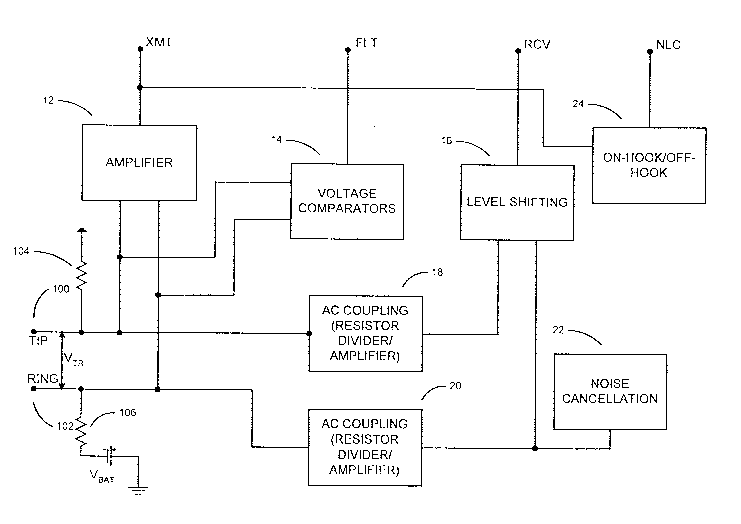
Resistive circuits are provided at the tip and ring of the battery feed circuit as
a method of alleviating the need for bulky DC transformers or complex integratedcircuitry. The voltage is monitored through a set of comparators eliminating theexpense of maintaining fused resistors. The voltages for voice or data transmission is
amplified prior to being transmitted. Received signals are AC coupled, with proper
biasing, onto the tip and ring lines. Any AC noise on the tip and ring line is shifted
180 degrees out of phase and re-inserted on the line to cancel the noise. As an
enhancement to the battery feed circuit, another voltage comparator is added to check
the line for DC current signifying an off hook condition.

Revendications

Note : Les revendications sont présentées dans la langue officielle dans laquelle elles ont été soumises.


- 5 -
CLAIMS:
1. A circuit for supplying direct current for a two-wire communication
transmission path comprising:
a resistive feed circuit supplying said direct current to said transmission
path,
tip and ring amplification means for sourcing and sinking current for
respective conductors of a telephone line,
an amplification circuit for transmitting said communication;
voltage protection means for guarding against an overvoltage condition;
and
an AC coupling network for receiving said communication.
2. The circuit of Claim 1 further comprising an AC noise cancellation
circuit for attenuating battery noise signals.
3. The circuit of Claim 2 wherein said AC noise cancellation is
accomplished by 180 degree phase shifting, amplifying and re-injecting said battery
noise signals into said transmission path.
4. The circuit of Claim 1 further comprising a means of monitoring on
hook/off hook of said telephone line.
5. The circuit of Claim 4 wherein said means of monitoring on hook/off
hook is a voltage comparator circuit.
6. The circuit of Claim 1 wherein said tip and ring amplification means
includes a capacitance means blocking DC voltage.
7. The circuit of Claim 6 wherein said capacitance means is at least one
capacitor.
8. The circuit of Claim 7 wherein said at least one capacitor is polarized.
9. The circuit of Claim 1 wherein said AC coupling network includes AC
biasing circuitry.
10. The circuit of Claim 1 wherein said voltage protection means is a
plurality of voltage comparators.

Description

Note : Les descriptions sont présentées dans la langue officielle dans laquelle elles ont été soumises.


~1~117~
BATTERY FEED CIRCUIT
BACKGROUND OF THE INVENTION
1. Field of the Invention
This invention relates generally to a battery feed circuit for telecommunications and
5 more particularly to a low cost battery feed using resistors.
2. Description of the Related Art
A battery feed circuit supplies a DC feed circuit to telecommunications equipment
through a 2-wire tr~nsmission path that also typically conducts a bi-directional voice
or data signal. The feed current is balanced, i.e., each tr~n~mission wire conducts a
10 current that is equal in magnitude but opposite in direction to the other.
A variety of battery feed circuits have been developed. In general, these circuits can
be grouped into one of two classes depending on their battery feed profile, that is the
relationship between the DC feed circuit and the voltage across the 2-wire tr~n~mi~sion
path. The first class of battery feed circuits produces a linear battery feed profile, e.g.
15 U.S. Pat. No 4,004,109 to F. S. Boxall, having a low common mode impedance tolongitudinal signals. The second class of battery feed circuits, such as those disclosed
in publication "A Floating Low-Power Subscriber Line Interface" by L. Freimanis and
D. P. Smith, ISSCC Di~est, 1980, pages 180, 181, provide a non-linear battery feed
profile which limits feed current on short 2-wire transmission paths. The noise
20 induced by longitudinal signals is minimi7ed by providing a high common mode
impedance through the use of isolation devices, e.g. transformers or opto-isolators.
These devices, however, tend to be bulky and expensive. One prior art attempt to deal
with this problem is in U.S. Pat. No. 4,476,350 to Aull et al. by the use of
bi-directional current sources.
25 SUMMARY OF THE INVENTION
In accordance with the principles of the present invention, the resistive feed circuitry
alleviates the need for bulky DC transformers or expensive, complex integrated

216~ ~L70
circuitry. The resistors are used in conjunction with a set of voltage omparators to
monitor for shorts or erroneously crossed voltage signals on the line. The comparator
circuitry eliminates the need to use fused resistors, thus, elimin~ting the expense of
having to replace the fuses as well as tracking down the cause of the fault. Once the
5 comparators detect a fault, the line can be opened with a relay device, until the cause
of the fault is found, preventing any damage to the circuitry.
Added features of the present invention is the ability to easily detect when the phone
receiver is on-hook or off-hook, and the cancellation of AC noise on the battery.
These features in combination with the resistor feed and comparator circuitry form a
10 relatively small, inexpensive means to comprehensively provide a DC current and an
AC signal to a telephone line.
BRIEF DESCRIPTION OF THE DRAWINGS
So that one skilled in the art to which the subject invention appertains will better
understand how to practice the present invention, preferred embodiments of the
15 apparatus and method will be described in detail hereinbelow with reference to the
drawings wherein:
Fig. 1 is a schematic block diagram of a battery feed circuit in accordance with the
present invention, and
Fig. 2 is a detail schematic diagram of Fig. 1.
20 DETAILED DESCRIPTION OF THE PREFERRED EMBODIMENTS
Fig. 1 illustrates, in a simplified manner, the desired operation of the resistive
feed architecture shown generally at 10. The input DC voltage to supply the loop DC
feed circuit is applied across the DC feed resistors 104 and 106. They provide
approximately 600 ohms of AC and DC impedance across the tip 100 and ring 102.
2 5 Any data or voice signals coming from a phone through the tip 100 and ring 102 will
be amplified via amplifier circuitry 12 before being transmitted on the line. At the
same time, any signal on the loop is being compared to a reference voltage in the
voltage comparator circuitry 14. This circuitry is monitoring for an over-voltage
condition on the line. Any data or voice signal that is to be transmitted to the loop
30 goes through level shifting circuit 16 and the resistor divider/amplif1er circuits 18 and

'~161170
20 which block the DC while amplifying and coupling the AC signals being sent tothe tip 100 and ring 102 of the telephone line. All the signals on the tip 100 and ring
102 lines are cleared of AC noise through the noise cancellation circuity 22. The on-
hook/off-hook circuitry 24 monitors the line to determine whether the user's phone is
5 on or off hook.
Now referring to Fig. 2, the feed resistors 104 and 106 which supply the DC
feed current to the loop from the input DC voltage are equal at 325.6 ohms each.This, together with resistors 110 and 114, provides the 600 ohm termination resistance
across the tip 100 and ring 102. The differential amplifier 128 provides an output
0 voltage equal to the differential voltage across the tip 100 and ring 102, Vtr, times the
value of the ratio of resistors 126 and 120. The value of input resistors 120 and 122
are equal, and the values of ground resistor 124 and feedback resistor 126 are also
equal. The voltage output of differential amplifier 128 represents both the differential
DC voltage and the AC voltage on the tip 100 and ring 102. This output voltage is
5 coupled to the transmit side of a 4-wire interface, where the DC is blocked thereby
allowing only transmission of the AC component. The output voltage of the
differential amplifier is also divided by resistors 130 and 132 and fed into a set of 12-
volt voltage sources 134 and 138. Two additional voltage sources 142 and 146 areconnected to the battery voltage attenuated by resistors 204, 202, 200 and 198. The
20 inputs to the differential amplifier 128 are compared against these sources using four
voltage comparators 136, 140, 144 and 148. The comparators indicate a fault if the
absolute value of the voltage across either feeding resistor 104 or 106 exceeds 36 volts.
The maximum should normally never exceed 24 volts as Vbat normally is 48 volts.
Transistors 152 and 156, along with transistors 174, 176 and 178, form a
25 differential amplifier. Those, in conjunction with current sources 150, 154 and 180
and resistor 155 couple any AC data or voice voltages representing incoming or
receive signals to amplifiers 116 and 118. Amplifiers 116 and 118 are of equal gain
but opposite phase, providing complementary drive to the tip 100 and ring 102
terminal. Having equal gain is important to provide balanced signals at the tip 100 and
3 o ring 102 terminals. Buffer 160 allows for proper biasing through resistors 170 and 172

2161~7~
of the received AC data or voice. Resistor 110 and resistor 114 form resistor dividers
going to the tip 100 and ring 102 and capacitors 108 and 112 capacitively couple the
signals from amplifiers 116 and 118, blocking the DC voltage. The capacitors 108 and
112 also reduce the quiescent power.
By blocking the DC current from the output of amplifiers 116 and 118,
polarized capacitors can be used because the DC bias of amplifiers 116 and 118 is half
supply voltage. In a fault condition, the capacitors 108 and 112 could become reverse
bias, but resistors 110 and 114 prevent any damage.
Differential amplifier formed by transistors 188, 190, 192 and 194, with currentsources 182 and 184, resistor 208 and capacitor 206, inverses the base of any noise on
the battery and re-injects it through amplifier 118 into the ring line to cancel the noise.
Resistors 202 and 204 divide Vbat by two for Vcm. Resistor 200 further
divides Vbat by three-sevenths for the reference input to comparator 196, and resistor
198 divides Vbat by three for the reference input to the voltage comparators 144 and
148. Comparator 196 indicates whether the phone is on-hook or off-hook via NLC
(Not Loop Closed).
Although the subject invention has been described with respect to preferred
embodiments, it will be readily apparent to those having ordinary skill in the art to
which it appertains that changes and modifications may be made thereto without
2 0 departing from the spirit or scope of the subject invention as defined by the appended
claims.

Dessin représentatif
Une figure unique qui représente un dessin illustrant l'invention.
États administratifs

2024-08-01 : Dans le cadre de la transition vers les Brevets de nouvelle génération (BNG), la base de données sur les brevets canadiens (BDBC) contient désormais un Historique d'événement plus détaillé, qui reproduit le Journal des événements de notre nouvelle solution interne.

Veuillez noter que les événements débutant par « Inactive : » se réfèrent à des événements qui ne sont plus utilisés dans notre nouvelle solution interne.

Pour une meilleure compréhension de l'état de la demande ou brevet qui figure sur cette page, la rubrique Mise en garde , et les descriptions de Brevet , Historique d'événement , Taxes périodiques et Historique des paiements devraient être consultées.

Historique d'événement

Description Date
Demande non rétablie avant l'échéance 1999-05-25
Inactive : Morte - Aucune rép. dem. par.30(2) Règles 1999-05-25
Inactive : Renseign. sur l'état - Complets dès date d'ent. journ. 1999-02-08
Réputée abandonnée - omission de répondre à un avis sur les taxes pour le maintien en état 1998-10-26
Inactive : Abandon. - Aucune rép dem par.30(2) Règles 1998-05-25
Inactive : Dem. de l'examinateur par.30(2) Règles 1998-02-24
Demande publiée (accessible au public) 1996-06-20
Toutes les exigences pour l'examen - jugée conforme 1995-10-24
Exigences pour une requête d'examen - jugée conforme 1995-10-24

Historique d'abandonnement

Date d'abandonnement Raison Date de rétablissement
1998-10-26

Taxes périodiques

Le dernier paiement a été reçu le 1997-08-27

Avis : Si le paiement en totalité n'a pas été reçu au plus tard à la date indiquée, une taxe supplémentaire peut être imposée, soit une des taxes suivantes :

  • taxe de rétablissement ;
  • taxe pour paiement en souffrance ; ou
  • taxe additionnelle pour le renversement d'une péremption réputée.

Les taxes sur les brevets sont ajustées au 1er janvier de chaque année. Les montants ci-dessus sont les montants actuels s'ils sont reçus au plus tard le 31 décembre de l'année en cours.
Veuillez vous référer à la page web des taxes sur les brevets de l'OPIC pour voir tous les montants actuels des taxes.

Historique des taxes

Type de taxes Anniversaire Échéance Date payée
TM (demande, 2e anniv.) - générale 02 1997-10-24 1997-08-27
Titulaires au dossier

Les titulaires actuels et antérieures au dossier sont affichés en ordre alphabétique.

Titulaires actuels au dossier
AT&T CORP.
Titulaires antérieures au dossier
DEWAYNE ALAN SPIRES
IAN ANDREW SCHORR
Les propriétaires antérieurs qui ne figurent pas dans la liste des « Propriétaires au dossier » apparaîtront dans d'autres documents au dossier.
Documents

Pour visionner les fichiers sélectionnés, entrer le code reCAPTCHA :


Pour visualiser une image, cliquer sur un lien dans la colonne description du document. Pour télécharger l'image (les images), cliquer l'une ou plusieurs cases à cocher dans la première colonne et ensuite cliquer sur le bouton "Télécharger sélection en format PDF (archive Zip)" ou le bouton "Télécharger sélection (en un fichier PDF fusionné)".

Liste des documents de brevet publiés et non publiés sur la BDBC .

Si vous avez des difficultés à accéder au contenu, veuillez communiquer avec le Centre de services à la clientèle au 1-866-997-1936, ou envoyer un courriel au Centre de service à la clientèle de l'OPIC.


Description du
Document 
Date
(aaaa-mm-jj) 
Nombre de pages   Taille de l'image (Ko) 
Description 1996-03-14 4 173
Revendications 1996-03-14 1 32
Abrégé 1996-03-14 1 18
Dessins 1996-03-14 2 42
Dessin représentatif 1998-05-11 1 14
Rappel de taxe de maintien due 1997-06-24 1 109
Courtoisie - Lettre d'abandon (taxe de maintien en état) 1998-11-22 1 184
Courtoisie - Lettre d'abandon (R30(2)) 1999-02-08 1 170