Note: Descriptions are shown in the official language in which they were submitted.
2 1 6 1 258
A COMMUNICATION METHOD FOR AN ADAPTIVE DIRECT
SEQUENCE CDMA COMMUNICATION SYSTEM
Te-hl~ir~l Field
This invention relates in general to the field of communication methods
and synchronization in data communication systems and more particularly to a
direct sequence code division multiple access (DS-CDMA) communication
system.
Background
Code division multiple access (CDMA) communication systems are used
extensively in satellite communications with military and co"~"efc;al
applications. These systems are also known as spread spectrum communication
systems because the communicated information is spread over a wide allocated
frequency spectrum. In CDMA communication systems the frequency spectrum
can be reused multiple times.
Rec~use CDMA modulation techniques are inherently more susceptible to
fading conditions present at the terrestrial and land mobile environments, theirapplication has been limited to satellite communications. However, with recent
advancements in communication signal processing, CDMA communication
systems are becoming increasingly popular in terrestrial land mobile
communication environments as well. For example, recent developments have
allowed CDMA systems to be used in cellular telephone communications
environments.
2 276~2~8
In general, there are two CDMA types of communication systems. One
is known as frequency hopping CDMA system where the wide allocated spectrum
is divided into a substantial number of narrower frequency band and information
signal is switched or "hopped" over these frequency bands in accordance with a
predetermined code. The other CDMA system is known as a direct sequence
CDMA communication system (DS-CDMA) where the user information signals
in the form of binary bits are spread over the allocated frequency spectrum by
combining them with spreading codes known as pseudorandom noise (PN) codes.
The spreading code comprises a predetermined sequence of binary states known
as chips. Thus, when combined, each user information bit interval gets coded
with a spreading chip sequence. Conventionally, a DS-CDMA transmitter
produces a direct sequence spread spectrum (DS-SS) communication signal by
multiplying the user information bit sequences by the spreading chip sequence.
Once received at a receiving end, the DS-SS communication signal is
decoded by multiplying the received signal by a despreading chip sequence
having co,lt;~onding characteristics to the spreading chip sequence. In
conventional DS-CDMA communication system, the receiver knows of the
spreading chip sequence prior to start of a communication call. Thereafter, the
receiver decodes the DS-SS communication signal based on the known spreading
chip sequence.
It is well known that in the presence of many users CDMA receivers in
addition to receiving the desired signal also receive many multiple-access
interfering signals. In presence of multiple access intelrerellce, reliable
communication may be achieved when interfering signals are received at
approximately the same power level. When there is a large disparity in received
signal powers, non-zero crosscorrelations among the signals gives rise to a
phenomenon known as near-far problem. In near-far situations, higher power
interfering signals significantly degrade reception and decoding of a lower power
desired transmission.
One conventional approach to improving the near far problem uses a
power control scheme where the powers from the receivers are fed back and
2 ~ 6 1 258
- 3 --
transmitter powers are controlled to substantially remove the power disparity.
In another approach, PN codes are constructed such that they provide
orthogonality between the user codes, thereby reducing mutual int~lrerence. Thisallows for higher capacity and better link performance, With orthogonal PN
S codes crosscorrelation is zero over a predetermined time interval resulting in no
intelrerence between the orthogonal codes provided only that the code time
frames are aligned with each other.
In conventional CDMA communication systems the spreading chip
sequence is either assigned by a self controller or it is pre-stored within the
receiving unit. As such, during despreading and demodulation process, the
receiver knows of the spreading chip sequence. A more recent approach for a
CDMA receiver proposes an adaptive despreading or demodulating process. In
an adaptive CDMA system, the receiver is enabled to ~lppless multiple access
interference by an adaptive equalization process. In such a system, a CDMA
transmitter transmits a training bit sequence which is coded with the spreading
chip sequence and the receiver adaptively determines, based on the training
sequence, the despreading code using a tapped delay line equalizer. Adaptive
del~"~ination of the despreading chip sequence and suppression of multiple
access intelrerence allows significant number of users to communicate with each
other over an spread spectrum channel without requiring central control
infrastructure, and as such paving the way for infrastructureless communication
systems.
However, in adaptive CDMA communication, the determined despreading
chip sequence is not time synchronized with the transmitter because of certain
time delays within the communication path or simply because the receiver does
not know when bit and chip timing of the transmitter starts. Conventional
methods of determining bit timing and chip timing offsets between the transmitter
and receiver comprise performing correlation routines involving complex
mathematical processing operations. These operations are time consllming and
therefore delay establishment of communication link between transmitter and
receiver. Therefore, there exists a need for a communication method which
21 61 258
-- 4 -
allows for quick establishment of communication links in an adaptive
communication system.
Sumrnary Of The Invention
Briefly, according to the present invention, there is provided a
communication method in a CDMA communication system having a transmitter
and a receiver. The trarlsmitter transmits a direct sequence spread spectrum (DS-
SS) communication signal comprising bit sequences coded with spreading chip
sequences, and the receiver receives the communication signal. The
communication method comprises the steps of, at the transmitter, spreading the
bit sequences including a training bit sequence with the chip sequence to produce
a spread bit sequence, modulating the spread bit sequence to produce a DS-SS
communication signal, and transmitting the DS-SS communication signal. At the
receiver, the DS-SS communication signal is received and demodulated. An
optimal despreading chip sequence is adaptively determined using the training bit
sequence during a training interval. After the training inteNal, chip timing offset
is determined during a chip timing interval to perform bit synchronization. After
the chip timing interval, bit timing offset is determined during a bit timing
interval to perform bit synchronization. Thus, the modulated DS-SS
communication signal is despreaded.
Brief Des~ tion Of The Drawings
FIG. 1 is a diagram of a CDMA communication system according to
present invention.
FIG. 2 is a timing diagram of a DS-SS communication signal according
to present invention.
FIG. 3 is a block diagram of a CDMA transmitter used in communication
system of FIG 1.
FIG. 4 is a block diagram of a CDMA receiver used in the
communication system of FIG 1.
2 1 6 1 258
FIG. 5 is a block diagram of a spreading equalizer transmitter used in the
receiver of FIG 4.
FIG. 6 is an exemplary timing diagram of a transmitter bit interval coded
with a spreading ehip sequence.
FIGS. 7-10 are exemplary timing diagrams showing effects of various
ehip timing offsets on output of a ehip matehed filter used in the receiver of FIG.
4.
FIG. 11 is a timing diagram of decoded DS-SS eommunication signal of
FIG. 2.
FIGS 12 - 13 are exemplary timing diagrams of output of a summer used
in spreading equalizer of FIG.5 showing effeets of various bit timing offsets.
Detailed Desc I i~)tion Of The Preferred Embodiment
While the speeifieation eoneludes with elaims defining the fea~ul~s of the
invention that are regarded as novel, it is believed that the invention will be
better understood from a eonsideration of the following deseription in eonjunction
with the drawing figures, in which like referenee numerals are earried forward.
Referring now to FIG. 1, a eommunieation system 100 embodying the
prineiples of the present invention is shown. The eommun;eation system 100
ineludes a plurality of CDMA trans,~ 10 and a plurality of CDMA reeeiver
20 whieh eommunieate direet sequenee spread speetrum (DS-SS) eommunieation
signals 30. The DS-SS communication signal 30 eomprises a radio frequency
eommunication signal modulated with binary bits coded with spreading chip
sequence. The communication system 100 is an adaptive CDMA communication
system whereby the despreading chip sequence is adaptively determined after the
CDMA receivers 20 demodulates the DS-SS communication signal 30. As
deseribed later in detail, the reeeiver ineludes a tapped delay line equalizer whieh
adaptively determines the despreading chip sequence during a training interval.
Because the adaptive equalization is performed in presence of multiple access
interfering signals, it adaptively produces the despreading chip sequence which
A
6 21 61 258
suppresses the effects of the multiple access interference and decodes the DS-SScommunication signal 30. Once CDMA receiver 20 determines the despreading
chip sequence communication between the CDMA transmitter 10 may be carried
on based on the determined despreading chip sequence provided the bit timing
and chip timing are synchronized.
In the present invention, the adaptive equalization during training is
performed without bit timing or chip timing synchronization of the receiver and
the transmitter. This is because perforrning synchronization of any kind in
presence of interfering signals is close to impossible. Thus, a redundant training
bit sequence is transmitted to circumvent the need for synchronization while thedespreading chip sequence is being determined during training interval.
Referring now to FIG. 2, a timing diagram of the DS-SS communication
signal 30 as transmitted by the transmitter 10 of FIG. 1 is shown. The DS-SS
communication signal 30 comprises string of bits which are coded with a
spreading chip sequence. The bits and the chips are binary signals ~suming one
of two states of +l and -1 represented by voltage potentials of V+l and Vl,
respectively. The V+l and V l potentials are of equal magnitude but opposite
polarity. In this description, it is assumed that V+l has a positive polarity and
the V l has a negative polarity. At the start of the DS-SS signal 30, a trainingsequence 31 is transmitted which is used by the receiver 20 to adaptively
determine despreading chip sequence using a tapped delay line equaliær based
on the training bit sequence. In the preferred embodiment of the invention, the
training bit sequence comprises a predetermined redundant bit sequence having
a non-altemating and continuous bit states, such as a sequence of consecutive + 1
bit state. The training sequence 31 is followed by a transmitter bit timing
sequence 33 which is used to synchronize receiver and transmitter bit timing.
The transmitter bit timing sequence 33 is predetermined bit sequence having
characteristics which gives the receiver information relating to the transmitter bit
timing. As described later in detail, the transmitter bit timing sequence 33
comprises an alternating bit sequence having alternating bit states of both + 1 and
-1. Following the transmitter bit timing sequence 33, a user information
-7- 2~ 61 258
sequence 35 comprising user generated data is transmitted. The user generated
data carries the actual data for communication of which the tr~n~mi~ion was
initi~t~d. The user generated data may for example be coded voice or raw binary
data.
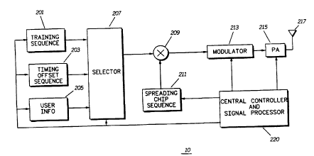
Referring now to FIG. 3, a blocked diagram of the CDMA transmitter 10
is shown. The CDMA transmitter 10, includes a central controller and signal
processor block 220, which controls the entire operation of the transmitter 10
including signal pr~cessing necessary for modulating and generating the spreading
chip sequence. The transmitter 10, includes a training sequence block 201 which
generates the predetermined training sequence. The transmitter 10 also includes
a transmitter bit timing sequence generator block 203 which generates the
transmitter bit timing sequence following the training sequence. Finally, a userinformation sequence block 205 provides user information in form of binary bit
sequences. The user information may be origin~ted from a variety of sources,
such as from a voice coder which receives voice information from a microphone
or it may comprise raw data information generated from a co",puling device. A
selector block 207 under the control of the central controller and process block220 provides for selecting one of the training, bit timing or user information
sequences in proper order and applies it to a multiplier 209. A spreading chip
sequence generator block 211 generates the spreading- chip sequence to be
combined with the bit sequence to be tr~nsmitted to the receiver. Perferably, the
generated spreading chip sequence comprise well-known gold PN codes having
desirable crosscorrelation and auto-correlation properties. The spreading chip
sequence has a predetermined number of chips (n) for coding each bit of the
transmission sequences. The multiplier 209 multiplies one of the transmission
sequences by the spreading chip sequence and applies it to a modulator 213.
Modulator 213 may comprise a number of well known binary signal modulators,
such as binary phase shift keying (BPSK) or quadrature phase shift keying
(QPSK) modulators. Output of the modulator 213 is applied to a power amplifier
215 which amplifies the modulated signal and applies it to an antennae 217 for
transmission. It may be appreciated that the block 220 and some of the other
2 1 6 t 258
blocks described in conjunction with transmitter 10 may be implemented utilizingone or more of well known digital signal processors, such as DSP 56000 series
manufactured by Motorola Inc.
Referring now to FIG. 4, the block diagram of the CDMA receiver 20 is
shown. The spread spectrum communication signal is received at the antennae
301 and is applied to a preselector filter 303 which provides the initial receiver
selectivity. The filtered signal is applied to a well known base band demodulator
305. The base band demodulator 305 comprises a well-known demodulator that
demodulates the communication signal in accordance with the modulation scheme
used in the transmitter 10 to provide a baseband signal 306. The base band
signal 306 is applied to a well-known chip matched filter block 307. The chip
matched filter comprises a well-known integrate-and-dump or a low pass filter
block where the received DS-SS communication signal 30 is sampled and
inleg,dted at chip rate and the result is dumped at the end of each chip interval.
The output of the chip matched filter is applied to a despreading equalizer 400
which, based on the training sequence adaptively determines a despreading chip
sequence. As described later in detail, the despreading equalizer provides
despreading chip sequence by adaptively eq~li7ing the detected coded bits with
an uncoded pre-stored signal corresponding to the training bit sequence. A signal
processor and controller block 320 performs all necessary signal proces~ing
requirements for the receiver 20. The equalizer 400 despreads the DS-SS
communication signal 30 and provides a decoded communication signal at its
output (415). The decoded communication signal is applied to a user interface
block 313 which may comprise one of a number of user interface devices such
as a speaker, a computing device, a data display or a fax or voice mail machine.
Referring now to FIG. 5, a block diagram of the despreading equaliær
400 is shown. The equalizer 400 comprises an n-tap delay line equalizer where,
as mentioned before, n is the number of chips per bit in the spreading chip
sequence. The tap delay line consists of a bank of n-1 serially coupled flip-flops
402 with their outputs coupled to a corresponding number of multipliers 404.
A
2~ 61 258
g
The bank of serially coupled flip-flops 402 operate as a shift register sequentially
shifting, at the chip rate, sampled outputs of the chip matched filter 307, i.e., (rl-
rn) during each bit interval. At the end of each bit interval, the multipliers 404
multiply the flip-flop out-puts with tap coefficients Cl-Cn provided by a tap
coefficient generator block 407. A summer 405 sums the outputs of the
multipliers 404 to provide the summer output 408. As such, the summer output
408 lel)r~sents integration of the multiplier outputs over one bit interval. Thesummer's output 408 is applied to a comparator 409 and a threshold decision
block 410. The threshold decision block 410 comprises a threshold co-l-paldtor
which after training interval provides the detected bits of the user bit sequence.
The threshold decision block 410 provides the equalizer output 415 The thresholddetector decision block 410 determines the decoded bit state by col,.pa,ing the
summer output 408 with a bit state threshold level. It may be appreciated that
the equalizer output 415 and the summer output 408 are related by having a (l/n)ratio therebetween.
During training, the col--palalor 409 Colll~'es the sl~mm~or~s output 408
with a pre-stored sequence as provided by a block 403. The pre-stored training
sequences is a pre-determined signal representing uncoded training sequence.
Therefore, the training sequence comprises a signal simulating uncoded redundantconsecutive and non-alternating training bits. The comparator 409 compares the
pre-stored training sequence with the summer output and provides an error signal411 which is applied to a tap coefficient generator block 407. The tap coefficient
generator blocks uses either the Least Means Square (LMS) or Recursive Least
Square (RLS) algorithm to update tap coefficients Cl-Cn once every bit interval
in order to minimize the error signal 411. The despreading equalizer 400
updates the tap coefficient C,-Cn until the error signal between the detected bit
sequence and the pre-stored training sequence is minimized. Hence, equ~li7ing
the summer output 408 with the output of the pre-store training sequencè. As a
result of equalizing the transmitted training bit sequence and the pre-stored
sequence, the tap coefficients C,-Cn become a representation of the despreading
chip sequence which despread the DS-SS communication signal 30 and suppress
2 1 6 1 258
- 10 -
multiple-access interfering signals without prior knowledge of the spreading chip
sequence. As such, the tap coefficients Cl-Cn represent of the despreading chip
sequence. These coefficients are used to despread the DS-SS communication
signal 30 after the training interval has terminated.
Operationally, upon commencement of a transmission the receiver
receives the training sequence 31 of the DS-SS communication signal 30 of FIG.
2. As mentioned, the training sequence comprises a bit sequence comprising
non-alternating bit sequence, such as a bit sequence having continuous coded
states of either +l or -1. Commlqn~urate with the training sequence, the pre-
stored sequence also p,~sen~ continuous uncoded states of either + 1 or -1 during
the training interval. When received, the training sequence is sampled at chip
rate via the chip matched filter 307. The output of chip matched filter is applied
to the tapped delay line equalizer 400 where through recursive iteration of
updating the tap coefficients C,-Cn the pre-stored training bit sequence and
detected bit sequence are equ~li7ed. When equalized, the produced tap
coefficients Cl-Cn result in decoding or despreading of the DS-SS communication
signal 30 and elimin~ion of the multiple access interfering signals. As such, the
equalizer 400 produces tap coefficients Cl-Cn which are a l~r~senlation of the
despreading chip sequence. Accordingly, the DS-SS communication signal 30
is decoded by adaptively dele,lnining a representation of the despreading chip
sequence based on the training bit sequence.
After the despreading chip sequence is determined the resulting tap
coefficients despread the received DS-SS communication signal while also
eliminating the interfering signals. It may be appreciated that after the training
interval the summer's output 408 at the end of each receiver bit interval
represents integration of the decoded communication signal over that receiver bit
interval. The integration, as herein described, constitutes summation of
multiplication result during discrete chip intervals. Ideally, when the equ~li7ing
tap coefficients (Cl-Cn) are determined after training, their multiplication by the
chip matched filter outputs (r,-rn) despreads or decodes the incoming DS-SS
communication signal. Therefore, the summer's output 408 after each receiver
- 11 - 21 6 1 258
bit interval is equal to the number of chips (n) multiplied by the bit potential of
the decoded communication signal bit, i.e. V+" or V, depending on the detecte~l
bit state, i.e., whether the detect~d bit comprises +1 or -1.
It may be appreciated that the tap delay line equalizer 400 could be
implemçnted within the digital signal processor 320 of the receiver 20. As such
the digital signal processor includes despreading means, determination means,
co".palison means and any and all other means necessary for processing and
controlling to effectuate the required functions of the present invention as
outlined in this specification. Alternatively the equalizer 400 may be
implemented 11tili7.ing conventional digital and logical discrete components as is
well known in the art.
llse of propagation delays and the fact that the receiver does not have
any information relating to the start of a tr~n.~mi~sion, a probable discrepancybetween the receiver and the transmitter timing may exist after completion of the
training interval. This timing offset may exist both for chip timing and bit timing
of the receiver. Therefore, the despreading chip sequence as provided by the tapcoefficients Cl-Cn may have to be synchronized for proper despreading of the
DS-SS communication signal 30. In the adaptive CDMA communication system
of the present invention, after the training interval, a chip timing offset estim~tion
is made during a chip timing interval. This is because, as described hereinafter,
the chip timing offset information could be extracted from the tap coefficients of
the equalizer.
Chip Tilning Offset
According to chip timing aspect of the present invention, the voltage
potential or the energy stored in the tap coefficients C,-Cn includes chip timing
information provided that the effects of the interfering multiple access signals are
suppressed. As described before, the despreading chip sequence is r~lesented
by the tap coefficients C,-Cn and potentials thereof. In the communication system
100, the interfering signals are eliminated after the training interval and upon
A
- 12- 21 61 258
determination of the despreading chip sequence. Therefore, chip timing offset
determination is commenced following the training interval to align receiver andtr~n~mitter chip timing. The chip timing offset determination process of the
present invention could take place during one or more bit intervals after the final
S tap coefficients are determined.
Referring now to FIG. 6, an exemplary chip sequence during one bit
interval is shown. The chip sequence comprises n chips which assume one of
two states + 1 and -1. Rec~l~$e the outputs of the chip matched filter 305 (rl-rn)
when sampled by the receiver contain information relating to the receiver and the
tr~n.cmitter chip timing offset and because the voltage potentials representing the
tap coefficients are directly propol lional to the energy of the received chips at the
end of receiver chip intervals, the tap coefficient potentials are processed fordetermining the timing offset. Due to binary nature of the chip sequence, the
ratio of the maximum potential of the outputs of the chip matched filter 307 to
the minimum output potentials relates to the chip timing offset. According to the
invention, the tap coefficients potentials can be divided into two sets: one having
maximum and another having minimum potentials. A first set of coefficient
potentials coll~ onds to those having maximum potentials (Vm~",) and a second
set of coefficient potentials coll~onding to those having minimum potentials
(V,"~). It has been determined that the voltage potential of tap coefficients insecond set change with respect to the tap coefficients in the second set by a factor
of (1-2 a), where a lt;presenl~ the chip timing offset in terms of one chip interval.
As such the following relationship exists between the chip timing offset and thetap coefficient voltage potentials:
a = % * (1- ¦ V m~ ¦ / ¦ V mar I ) E~ . ( 1 )
Therefore, by examining the tap coefficient potentials relating to each set the chip
timing offset may be determined. It should be noted that in equation 1 the
maximum potentials and the minimum potentials are expressed in terms of
21 6~ 258
absolute values. Therefore, their polarity is irrelevant for determination of chip
timing offset.
To illustrate the above concept, a number of exemplary situations where
the receiver bit timing off set is equal to zero lh chip interval, + 1/4 chip interval
S and -174 of chip interval will be examined.
FIG. 7 shows the output of the chip matched filter 307 as it samples at
chip rate, integrates during the chip interval, and dumps at the end of the chipinterval when the transmitter chip timing and receiver chip timing are
synchronized, that is, chip timing offset =0. As shown, the output of the chip
matched filter at the end of each intervals 701-707 has one of two equal but
opposite potentials V+l and V ,. the potentials correspond respectively to either
of the + 1 or -1 potential of the chip state. Re~use the sampled values rl-rn are
directly proportional to the tap coefficients Cl-Cn, the absolute value of the first
set of coefficient potentials, i.e., ¦ V",~" ¦, is equal to the absolute value of the
lS second set of potentials, i.e., l Vmjn l . Therefore, the ratio of
I Vmjn I / I V""Lr I is equal to 1 resulting in a timing offset determination of a=0
according to equation 1. As such, the timing offset may be determined by
processing the tap coefficient potentials at the end of each bit interval. It should
be noted that Vm~,~ (or Vmjn for that matter) as referred herein could be considered
as co-lesponding to either one of V+l or V l since the absolute values of the Vm~x
or Vmjn are of significance equation (1).
Referring to FIG. 8, a receiver chip timing offset of 1/2 chip is assumed.
That is, the chip interval 701 is half a chip off from the chip interval 801. Asshown, the output of
chip matched filter at the end of time interval 801 reaches V+l. Then at the endof time interval 802 the chip matched filter output reaches a zero potential. Atthe end of chip interval 803, the output reaches V ,. Again, at the end of chip
intervals 804-806, the outputs are at zero. And finally at the end of interval 807
the output reaches V+,. Accordingly, the first set of coefficient would have a
potential V",~ which is equal to V+, (i.e., V m~"=V+I (or V ,)) and the second
set of coefficients Vmin would have a potential equal to zero (i.e., Vmin=O).
21 61 258
- 14 -
Therefore, from equation (1) a chip timing offset of a=l/2 chip interval would
result.
Referring to FIG. 9, a receiver chip timing offset of +1/4 iS
assumed. The positive sign of the chip timing offset signifies that the transmitter
chip timing leads the receiver chip timing. That is, the transmitter chip timingreference starts prior to the receiver chip timing reference. Following the above
analysis V",~,~, is equal to V+, (or V l) and Vm" is equal to l/2 of V+l. As such,
the equation (1) yields a timing offset a=l/z chip timing.
The timing offset determined based on Equation (1), however,
does not provide information relating to whether the timing offset is positive or
negative. The sign of the timing offset indicates whether the receiver chip timing
is leading or trailing the transmitter timing offset. According to the invention, the
sign of information can be determined by ex~mining the polarity and magnitude
of successive tap coefficient potentials during one bit interval or two successive
bit intervals. Therefore, once the absolute value of the timing offset a is
determined further proceccing of the tap value coefficients results in
determination of the timing offset sign.
It may be appreciated that when the timing offset is equal to l/2
chip interval the sign of the offset becomes irrelevant since the receiver chip
timing could be adjusted by one half chip interval in positive or negative
direction resulting in synchronization with transmitter chip timing. Furthermore,
positive chip timing offset of greater than l/2 chip timing offset could be
expressed in terms of a negative complementary offset. For example, a positive
3~4 timing offset could be expressed as a - Ih timing offset and so on. Therefore,
the timing offset a would be a value within the range of zero to l/2 with the offset
timing sign signifying the leading or trailing status of the receive chip timingoffset.
Referring to FIG. 10, a receiver chip timing offset of 1/4 is`shown.
In order to better understand the process by which sign of the timing offset maybe determined, the --lh timing offset of FIG. 10 will be compared with the + 1/4timing offset condition of FIG. 9. As can be seen in FIG. 9, during consecutive
A
2~ 6t 258
- 15 -
intervals 901, 902 and 903, when there is a transition from a V+l to a V l (chiptransition of positive potential to negative potential), the outputs of the chipmatched consist of V+l, l/2 V+l, and V l. Due to the fact that the timing offsetis positive in FIG. 9, after completion of a positive to negative chip transition
occurring during intervals 601 to 602 (shown in FIG. 6), the output of the chip
matched filter reaches a positive polarity, i.e., l/z V+" at the end of interval 902.
Conversely, in FIG. 10, because of negative timing offset, the output of the chip
m~tched filter after completion of the same positive to negative chip transitionwould reach a negative polarity, ie., l/z Vl, at the end of interval 103.
Therefore, the sign of the timing offset could be determined based on the polarity
of at least one of the tap coefficient potentials after one or more chip transitions.
It may be appreciated that the same type of analysis is applicable to a negativeto positive chip transition as well as other chip sequence arrangements.
The tap coefficient potential processing needed for d~le~ ination
of the chip timing offset a and its sign could all be accomplished by a~ropliately
progr~mming the digital signal processor 320 utilizing well known signal
proces~ing techniques. As such the signal processor 320 includes means for
determining chip timing offset based on the tap coefficient potentials as well as
the means for determining sign of the chip timing offset based on the polarity of
at least one of the tap coefficients after a chip transition.
Upon determination of the chip timing offset and sign thereof, the
receiver chip timing could be adjusted to synchroniæ it with the transmitter chip
timing. It should be noted that because of existence of multiple access
interference the chip timing offset determination according to the present
invention produces an estimate and not the precise chip timing offset. Therefore,
there may still be a need to perform some minor correlation routines to completechip synchronization. However, the amount of time needed to perform such
routines is minimal. Once the chip timing synchronization is performed, the
receiver 20 commences a bit timing synchronization process during a bit timing
interval.
- 16- 21 61 258
BIT TIMING OFFSET
Rcc~use of redundancy of the training sequence no synchronization
is necessary during training interval. Ass~lming that the chip timing is
synchronized, bit timing offset between the receiver and the transmitter during
the training interval causes the resulting tap coefficients Cl-Cn, which ~lesents
the despreading chip sequence, to be cyclically shifted by a corresponding
number of chips. Therefore, the receiver bit timing offset may be e~ ssed in
terms of chip numbers.When the DS-SS communication signal 30 is despreaded,
after the determination of tap coefficient Cl-Cn the resulting decoded DS-SS
communication signal includes bit timing information which may be extracted in
conjunction with the transmitter bit timing sequence 33 of FIG. 2.
After the training interval, the summer output 408 provides a
~preser~tion of the decoded DS-SS communication signal 30. Therefore, the
summer output 408 is processed to determine the bit timing offset.
It has been determined that the following relationship exists
between the bit timing offset and the summer output:
y,=bt, (n-m) + bl(m) Equation (2).
Where Y, is the summer output at time t, b,, and b, are decoded bits at times t-l
and t, m is bit timing offset in terms of number of chips, and n is number of
chips per bit. When b, l and b, are consecutive non-alt~nating bits, then Y, is
equal to their bit state, i.e., either + 1 or -1. When b, ~ and bl, are ~lt~rn~tin~ bits
then Y,= +(n-2 m) if b,, = + 1 and b, = -1, and Yt= +(n-2 m) if b, l = -1
and b,= + 1. Accordingly, the bit timing offset information may be extracted by
procescing the summer output 408 after an alternating transition from one bit
state to another bit state has occurred.
Referring to FIG. 11, a decoded communication signal upon
completion of the training interval and after determination of the despreading
sequence is shown. As shown, the transmitter bit timing sequence 33 follows the
training sequence. The transmitter bit timing sequence when received, provides
the receiver 20 with the capability of detecting start of the transmitter bit interval.
The transmitter bit timing sequence 33 comprises a sequence of alternating bit
- 17- 21 61 258
sequence with at least two consecutive bits having alternating states such that the
state of one bit changes from one interval to the succeeding interval. In other
words, a transition from +1 to -1, or vice versa, would exist between two
consecutive bits from a first bit interval to the subsequent second bit interval. The
transitions occurring over the transmitter bit timing sequence are critical because
they are indicative of transmitter bit timing which is used in the receiver to
determine the bit timing offset according to equation 2. As shown, an exemplary
transmitter bit timing sequence may consist of the sequential bit states of +1,
+ 1, -1, -1, + 1, + 1, -1, -1 occurring respectively in transmitter bit intervals
111, 113, 11S, 117. It may be appreciated that the transmitter bit timing
sequence may be of other variety of sequences, such as alternating bit sequence
of + 1, + 1, -1, + 1, -1 as long as the sequence consists of transitions conveying
transmitter bit timing information.
In the plefell~d embodiment, the receiver bit timing offset is
determined after the training interval by integrating, over a first receiver bitinterval, non-alternating bits of the decoded communication signal to produce a
first result, and integrating over, a second receiver bit interval, alternating
consecutive bits of the decoded communication signal to produce a second result.Thereafter the first result is compared with the second result to
determine the bit timing offset. The bit timing offset is determined by
det~ll,lining half the difference between the first result and the second result. It
should be noted that the first result may be a prestored constant value
representing the result of integration over non-alternating bits.
The above concept may be better understood by referring to FIG.
12, where the summer output in a situation where the bit timing offset is -m
chips is shown. The negative sign of the timing offset indicates that the
transmitter bit interval occurs before the receiver bit interval. The normalizedoutput of the summer at the end of the first receiver bit intervals which` occurs
during the consecutive non-alternating bit states of + 1, corresponding transmitter
bit intervals 111 and 113, is equal to n, i.e. first result =n. The normalized
summer output 408 at the end of the second receiver bit interval after integration
A
2 1 6 1 258
- 18 -
during the alternating bit transition from + 1 to -1 occurring on the transmitter
bit interval 115 is equal to -(n-2 m), i.e., second result is n-2 m. Therefore, by
delellllining half the dirrer~nce between absolute values of the first result and the
second result the absolute value of the bit timing offset m is determined.
S The absolute value of the chip timing offset as determined above
does not indicate sign of the receiver bit timing offset. In order to better
understand the process by which the sign of bit timing offset is determined, an
exemplary situation where the receiver bit timing is equal to +m chips as shown
in FIG. 13, is compared to the situation of FIG. 12 where the receiver bit timing
is -m chips. In FIG. 12, during a positive to negative transition (occurring during
transmitter bit intervals 113 to 115), a negative bit timing offset produces a first
result which has a positive polarity and a second result which has a negative
polarity after the transition. Whereas, in FIG. 13, during the same positive to
negative transition, a positive bit timing offset produces a positive polarity first
result and second result. In another example, referring to FIG. 12th negative topositive transition from the transmitter bit interval 117 to 119, produces a
negative polarity first result (the polarity of the summer output as a result ofintegration of two consecutive -ls of intervals 115 and 117), and a positive
second result when the bit timing offset sign is negative. In FIG. 13, during the
same negative to positive transition, a positive bit timing offset sign producesnegative first and second results. As such, it may be appreciated that the sign of
the bit timing offset may be determined by determining the type of transition, i.e.
positive to negative or vice versa and comparing the polarities of the first result
and the second result. Accordingly, of the bit timing offset is determined by
comparing results of integration produced during consecutive non-alternating bits
with that obtained during alternating bits.
Upon determination of the bit timing offset and sign thereof, the
receiver bit timing could be adjusted to synchronize it with the transmitter bittiming. It should be noted that because of existence of multiple access
interference the bit timing offset determination according to the present invention
produces an estimate and not the precise bit timing offset. Therefore, there may
- 19- 21 61 258
still be a need to perform some minor correlation routines to complete bit
synchronization. However, the amount of time needed to perform such routines
is minim~l. Once the bit timing synchronization is completed, the receiver 20
commences to decode user information sequence.
As outlined above, the adaptive communication system 100
uniquely communicates DS-SS communication signal 30 from the transmitter 10
to the receiver 20 in three sequential intervals: first the training interval, then the
chip timing interval and finally the bit timing interval. The unique communication
sequence of the present invention greatly facilitates receiver and transmitter
timing synchronization in an adaptive CDMA communication system which
results in quick establishment of communication links between CDMA receivers
20 and the CDMA transmitters 10. First during the training interval, the
despreading equalizer 400 decodes the DS-SS communication signal 30 which
includes the training bit sequence. The DS-SS communication signal 30 is
decoded by adaptively determining, based on the training bit sequence, tap
coefficients of the equalizer which represent the despreading chip sequence. As
result of the training process, the effects of multiple access interfering signals are
eliminated paving the way for chip timing and bit timing offset determination.
Rec~use the bit timing offset information can be easily extracted following the
chip timing offset determination, therefore, after training interval the chip timing
offset is determined during the chip timing interval. The chip timing offset is
determined based on the potential of the representation of the despreading chip
sequence. Finally, during the bit timing interval, the bit timing offset is
determined based on the decoded DS-SS communication signal and the
transmitter bit timing sequence which is transmitted following the training bit
sequence.
While the preferred embodiments of the invention have been
illustrated and described, it will be clear that the invention is not so limited.
Numerous modifications, changes, variations, substitutions and equivalents will
-20- 21 61 258
occur to those skilled in the art without departing from the spirit and scope of the
present invention as defined by the appended claims.