Note: Descriptions are shown in the official language in which they were submitted.
~ 2 l 61 932 CFO 10992 CA
Photovoltaic Element and
Method for Producing The Same
BACKGROUND OF THE INVENTION
Field of the Invention
The present invention relates to a photovoltaic
element for a solar cell, a photo sensor and others,
and a method for producing the same.
Related Backqround Art
Solar cells applying photovoltaic elements are
expected as an alternative energy source for existing
power generation of fired power generation and
hydroelectric power generation solving the problems of
these conventional power generation. In particular,
various studies have been made on amorphous silicone
solar cells, because the cells can be made relatively
at low cost and can be produced as the elements that
have larger area than solar cells using crystalline
solar cell elements. Improvement of the photoelectric
conversion efficiency of amorphous silicone solar cells
is one of important problems for commercializing the
amorphous silicone solar cells. Studies have been made
ardently for solving the problems as shown hereunder.
The structure of amorphous silicone solar cell
elements is known in which back electrode,
semiconductor layer and incident surface electrode are
laminated in this order on a conductive substrate such
2161932
-- 2 --
as stainless plate. The incident surface electrode is
made, for example, by transparent conductive oxides.
Furthermore, a collector electrode comprising fine
metallic wire is placed on the incident surface
electrode mentioned above for collecting the generated
electricity. The collector electrode mentioned above is
provided on the incident surface; consequently it
reduces effective generating area of the solar cell.
The area loss is called shadow loss. For this reason,
the collector electrode mentioned above is usually made
in a fine comb shape. Thus, the shape of the collector
electrode normally tends to be fine and long shape, and
the selection of material and the design of cross
sectional shape are required so as to make the electric
resistance small.
An electrode called bus bar electrode is formed on
the surface of the collector electrode mentioned above,
for collecting the electric current that is collected
by the collector electrode. The bus bar electrode is
made from metallic wire that is thicker than the wire
of the collector electrode.
Now, the present situation of the research is
explained for minimizing shadow loss and loss by
electric resistance and for improving the conversion
efficiency of solar cell that is constructed as
described above.
Materials that have small resistivity such as
2161932
-- 3
-
silver (1.62 x 10⁻⁶ Qcm) or copper (1.72 x 10⁻⁶ Qcm) are
used for the above mentioned collector electrode to
reduce the shadow loss and electric resistance loss.
Vacuum evaporation, plating and screen printing
are used as the method to form the collector electrode.
The vacuums evaporation method has problems such
as slow sedimentation, low through put, caused by the
use of vacuum process, and necessity of masking to form
the linear pattern, and also the masking results in the
loss of metal, sediment on the masked portion. The
problem in the screen printing is the difficulty
forming low resistance electrode.
For example, the resistivity of the lowest
resistance of conductive paste is about 4.0 x 10⁻⁵Qcm,
this is the value one order higher than that of bulky
pure silver, this means resistance of the paste is
larger than that of the silver in one order. The
following three methods are used to reduce the
resistance without area reduction of the collector
electrode using such a material.
(a) Increasing the thickness of the electrode. In this
case, practically usable upper limit of the thickness
is 10 ,um to 20 ,um. When this thickness of electrode is
used to form a long, for example more than 10 cm,
collector electrode, it is necessary to make the width
of the electrode more than 200 ,um in order to keep the
electric resistance loss small, and the Aspect ratio
_ 4 _ 2 1 6 1 93~
(ratio of thickness and width) becomes small value such
as 1:10, and the shadow loss becomes larger.
(b) Collector electrode that is made by coating a
metallic wire with a conductive particle containing
polymer is proposed in USP 4,260,429 and USP 4,283,591.
The cross section of the collector electrode proposed
in the USP 4,260,429 is shown in Fig. lA. In this
figure, reference numeral 101 is a metallic wire, and
reference numeral 102 is a coated layer made of the
conductive polymer. This invention has a merit that
even the long electrode that is made using the copper
wire has small electric resistance loss, and the shadow
loss is also small because the Aspect ratio can be made
small value such as 1:1. The security of the collector
electrode proposed in the USP 4,260,429 is that the
wire can be fixed by a simple method using conductive
adhesive. A method to prevent physical contact between
the metallic electrode and Cu2S layer is proposed in USP
4,283,591, this method provides prevention of the
metallic copper deposition.
However, these proposals have following problems.
(1) In the case of USP 4,260,429.
A) Following problems were found by a long term
exposure test or by temperature-humidity tests that
short circuit between upper electrode and lower
electrode is formed in a defective part such as pin
hole or short circuit; lower conversion efficiency
_ 5 _ 2l 6l 932
results from the small shunt resistance, tends to get
worse yield. Experiments by the present inventors
showed that the problem comes from electro-chemical
reaction in which the ion component of the above
mentioned metallic wire diffuses through the conductive
polymer and reach the above mentioned semiconductor
element.
B) The electrode disclosed by USP 4,260,429
proposes to get good electro-conductivity between the
metallic wire and the semiconductor element, and the
solution of the problem that the occurrence of the
trouble by the electro-chemical reaction between the
metallic wire and the semiconductor element is not
included.
C) The electrode disclosed by USP 4,260,429 has a
problem that some portion of the electrode may have not
enough bonding force. In some occasion, tub of some
metallic material almost did not have enough bonding
force when the adhesive connection between the solar
cell substrate and metallic tub of the collector
electrode was required.
D) Not only initial bonding force but constant
bonding force between the electrode and the solar cell
is required for the solar cell used in open atmosphere
in severe condition. The solar cell that used
electrode described above had a problem that the series
resistance increase and the conversion efficiency
_ - 6 ~ 21 61 932
decrease caused by the deterioration of the bonding
force occurred during the temperature-humidity test and
the heat resistance test as the acceleration test.
E) Some problems of peeling off were observed on
the solar cell caused by the lack of initial bonding
force between the solar cell substrate and metallic
tub, and also by degradation of the bonding force
between the cell element, metallic wire and the coating
layer, affected by the humidity and temperature.
F) The solar cell was affected easily by the
humidity because tight covering layer was not formed as
the covering film.
G) It is desirable that the covered wire electrode
can be manufactured in off line and be used from the
storage, however, in the case where thermosetting resin
was used the above mentioned electrode had a problem
that it was difficult to obtain the enough bonding
force when it was formed on the solar cell because the
cure acceleration of the polymer after the drying up
was difficult to control. Furthermore there was no
means on the selection of the curing agent to cure the
thermosetting resin and relatively long curing time was
required.
H) When only thermoplastic resin was used,
deformation of the electrode occurred caused by the
thermo-hysteresis during the lamination process after
the formation of the electrode, and the following
2161932
_ - 7 -
problems were observed, line width change, partial
peeling and position shift of the electrode.
I) For the solar cell that is used in open
atmosphere, it is required that there is no change in
the bonding force between the electrode and the solar
cell element even if it is used for long term in severe
condition. The solar cell that used above mentioned
electrode had a problem that series resistance increase
and conversion efficiency decrease caused by the
deterioration of the bonding force during long time
open air exposure test or temperature-humidity test as
the acceleration test.
(2) In the case of USP 4,283,591.
A) Although the idea to prevent physical contact
between metallic electrode and semiconductor layer was
disclosed, but the solution of the problem, in which
the metallic ion diffuses slowly through the conductive
polymer and induces trouble, was not proposed.
B) The electrode proposed by this invention has
the possibility that the metallic wire may contacts
with the solar cell substrate as the result of breakage
of the above mentioned covering layer during the
thermal crimp process. The concrete counter measure of
this problem is not proposed.
C) The proposal has some limit in the electrode
formation because the procedure do not contain drying
process and the covered wire can not be stored.
- 8 -21 61 932
(3) In the cases of USP 4,260,429 and USP 4,283,591.
A) Either proposal has the problem that it is
difficult to get covering layer of uniform thickness
and stable good electric conductivity.
B) Short circuit between upper electrode and lower
electrode is formed when the covering layer has pin
hole that induces large enough leak current. As the
result the shunt resistance decreased, lower conversion
efficiency is resulted and the yield was decreased.
C) The electrode proposed by the invention has the
possibility that the metallic wire may contacts with
the solar cell substrate, and when it is used outdoors
enough effect of migration and shunt closure was not
obtained.
(4) In the case of USP 5,084,104.
A) Short circuit between upper electrode and lower
electrode is formed when an amorphous silicone solar
cell that has defective part such as pin hole or short
circuit was used, and lower conversion efficiency is
resulted from the small shunt resistance, tends to get
worse yield.
B) Series resistance of the electrode that is
covered by conductive adhesive increases by thermo-
hysteresis because of the solution or the softening of
the electrode caused by the penetration of the paint
solvent.
C) The series resistance of the photovoltaic
2161932
g
element increases and the conversion efficiency
decreases when it is tested by open air exposure test
or temperature-humidity test as the acceleration test.
SUMMARY OF THE INVENTION
An object of the present invention is to provide a
collector electrode that has excellent storability,
adhesiveness, and resistance to leak due to humidity.
Another object of the present invention is to
provide a photovoltaic element that has high initial
characteristic and long term reliability, using the
above mentioned collector electrode, can avoid short
circuit between the upper electrode and lower
electrode, can avoid penetration of the paint solvent
to the electrode covered by the conductive adhesive,
and can prevent the increase of resistance in series.
Still another object of this invention is to
provide a manufacturing process that can make the
photovoltaic element in a high yield and in stable
operation.
According to the first example of the present
invention, a photovoltaic element is provided of a
structure in which an electrode coated with a
conductive adhesive is placed on a photoactive
semiconductor layer through the conductive adhesive,
wherein the conductive adhesive is composed of at least
two layers; and the softening point of the conductive
2161932
-- 10 --
adhesive composing the layer nearer to the electrode is
higher than the highest temperature in the heat history
of the photovoltaic element.
According to the second example of the present
invention, a collector electrode is provided in which a
metal wire does not contact photovoltaic elements
directly because a coating layer comprising a
conductive resin is provided on to the metal wire,
wherein the metal ion of the metal does not diffuse
into the semiconductor layer of the photovoltaic
element.
According to the third example of the present
invention, a collector electrode in which a metal wire
comprising a coating layer consisting of a conductive
adhesive is formed with adhesion on photovoltaic
elements through said coating layer, wherein that the
metal ion of said metal wire does not diffuse into the
semiconductor layer of said photovoltaic elements.
According to the fourth example of the present
invention, a photovoltaic element which comprises a
semiconductor layer consisting of at least one pin
junction or pn junction and a collector electrode
provided in the incident side of the semiconductor
layer, wherein the collèctor electrode comprises the
collector electrode obtained in the second or third
example.
According to the fifth example of the present
- 11 21 61 932
invention, a method for manufacturing a photovoltaic
element of a structure having a collector electrode in
the incident side, wherein the collector electrode
obtained in the second, third or fourth example is
adhered to the incident face of the photovoltaic
element by means of heat, pressure, or heat and
pressure.
BRIEF DESCRIPTION OF THE DRAWINGS
Figs. lA and lB are schematic cross-sectional
views illustrating composition of a collector electrode
that is provided with a coating layer on the metal
wire, according to the present invention.
Figs. 2A, 2B and 2C are schematic cross-sectional
views illustrating composition of a collector electrode
having a plurality of coating layers and the fixation
condition of the collector electrode on to a substrate.
Fig. 3 is a schematic cross-sectional view
illustrating for a wire coat device used for
manufacturing a collector electrode of the present
invention.
Figs. 4A, 4B and 4C are schematic cross-sectional
views illustrating composition of a solar cell of
amorphous silicon type, according to the present
invention.
Fig. 5is a schematic cross-sectional view
illustrating composition of a solar cell of single
- 12 _ 21 61 932
-
crystal silicon type, according to the present
invention.
Fig. 6 is a schematic cross-sectional view
illustrating composition of a solar cell of polycrystal
silicon type, according to the present invention.
Fig. 7 is a schematic cross-sectional view
illustrating composition of a thin film solar cell of
polycrystal silicon type according to the present
invention.
Figs. 8A and 8B are schematic plan views
illustrating composition of a solar cell that is an
example of the photovoltaic element according to the
present invention.
Fig. 9 is a schematic cross-sectional view
illustrating composition of a photovoltaic elements
module using a collector electrode having two layers
coating, according to the present invention.
Fig. 10 is a schematic cross-sectional view
illustrating composition of a photovoltaic elements
module using a collector electrode having two or three
layers coating, according to the present invention.
Fig. 11 is a schematic cross-sectional view
illustrating composition of a photovoltaic elements
module using a collector electrode having three layers
coating, according to the present invention.
Fig. 12 is a graph showing the relationship
between volume resistivity and conversion efficiency in
- 13 _ 2 1 6 1 932
`
a module of photovoltaic elements according to the
present invention.
Fig. 13 is a schematic plan view illustrating
composition of another module of photovoltaic elements
using a collector electrode having the coating layer,
according to the present invention.
Fig. 14 is a graph showing the relationship
between steaming cycles and series resistance for a
module of photovoltaic elements according to the
present invention.
DETAILED DESCRIPTION OF THE PREFERRED EMBODIMENTS
According to experiments conducted by the
inventors, the problem arising in the formation of the
existing collecting electrode, during the process
following the coating and drying of the wire; in
environments where light and moisture are present; was
found to be caused by electromotive force being applied
to the collecting electrode, thereby diffusing ions
from the metal wire to the conductive resin layer.
Also, the problem of shunt with the existing collecting
electrode formation was found to be caused by the
possibility that the metalwire could contact the
semiconductor layer or the transparentconductive film,
because the conductive resin coating consisted of only
one layer. In other words, it is not possible, with
the existing collecting electrode, to prevent the metal
2161932
- 14 -
wire from directly contacting the semiconductor layer
without the inclusion of conductive resin during the
thermocompression bonding process and therefore, it was
found that contact of the faulty area and the wire was
the cause of the initial decrease in yield. In
addition, we have discovered that, even if such contact
was prevented, metal ion diffùsion occurred during
actual usage, because of minute pores in the conductive
resin, as well as the moisture and ion permeability of
the resin itself. We have also discovered that the
problem of long-term dependability was attributed to
the deterioration of conductivity with the conductive
resin, caused by oxidation of the metal wire surface
(consisting of copper, etc.), which is caused by
moisture penetrating during outdoor use, because the
polymer used in solar batteries laminated with polymer
is not perfectly water tight.
We have also found out that it is problematic that
the bridging density of the conductive resin layer
could not be controlled regarding the shelf life and
adhesive strength of the collecting electrode. In
other words, the problem was that, when curing resin is
used in polymers that form the conductive resins of the
existing collecting electrode, the resin would harden
after drying, for example during storage, while the use
of thermoplastic resin was also a problem because the
fluidity would become too large from the heat history
2161932
- 15 -
of later processes, because the resin will not bridge.
Furthermore, low resistance copper and aluminum
wires used in wiring for electric appliances are
inexpensive and good conductors. Enamel wires, etc.
are made by coating these metal wires with insulating
varnish, but generally, it is not easy to coat metal,
which are inorganic, with material that contains
organic material. In addition, sufficient adhesive
strength may not be obtained when adhering the wire,
through the coating layer, to semiconductors and
metals. This is because a special bond does no exist
between the organic material in the coating layer and
the semiconductor or metal material. This problem
becomes even more pronounced depending on the metal
material and its surface conditions, and we have
discovered that almost no adhesive strength can be
obtained when they are affected by moisture.
As a result of studies by the inventors of this
invention aimed at tackling these problems, we have
discovered that good adhesion, offering good storage
characteristics with no progressive curing after the
heat/drying process, can be achieved without altering
the shape of the electrode by using a curing agent,
such as block isocyanate, etc. to control the bridging
density of the conductive resin layer before and after
the process of forming the electrode on the surface of
the solar cell.
2161932
- 16 -
We were able to create solar batteries of good
characteristics by dividing the coating layer into
multiple layers, where each layer will be assigned
different jobs, such as preventing moisture and ion
permeation, and the adhesion of the metal wire to the
semiconductor layer or the transparent electrode.
Also, by creating a coating layer consisting of
polymer containing a coupling agent and conductive
filler, the surface of the metal was altered in such a
way that it will readily adhere to organic material,
whereby a good adhesion between the metal and the
conductive resin layer containing organic material was
achieved based on the knowledge of this invention.
Next, we will describe the constitutive
characteristics of the embodiment of this invention, as
well as the interactive effects based thereon.
(1) With regard to the collecting electrode on
which a metal wire; coated with a layer consisting of
conductive adhesive; is adhesion-formed on the
photovoltaic element through the layer of coating, we
have prevented the metal ions in the metal wire to
diffuse into the semiconductor layer of the
photovoltaic element. As a result, we were able to
prevent the short circuiting of the metal wire and the
semiconductor layer of the photovoltaic element, which
causes deterioration of the photovoltaic element's
exchange efficiency.
- 17 - 21 61 932
-
(2) Because the coating layer possesses the
property of preventing the diffusion of the metal ions,
it becomes possible to prevent the deterioration of the
photovoltaic element's exchange efficiency caused by
the short circuiting of the metal wire and the
semiconductor layer of the photovoltaic element, even
if the metal wire is applied with a voltage that is
greater than the photovoltaic element's electromotive
force, regardless of the voltage which is applied on
the metal wire.
(3) Because the conductive adhesive consists of
conductive particles and polymer, the resistivity of
the conductive adhesive can be variably adjusted
between 0.1 Qcm and 100 Qcm.
(4) The surface of the metal, for example, a
metal wire, is altered in such a way that it is readily
bonded to organic material and therefore providing a
good adhesion between metals and conductive resin
containing organic material, because the conductive
adhesive consists of a coupling agent, conductive
particles and polymer.
(5) Since one of the following; silane based,
titanate based and aluminum based coupling agents; will
be chosen as the coupling agent, it is possible to
control the interface between dissimilar material. In
other words, it will act as a medium between the
inorganic material (metal) and the organic material
- 18 -
2161~32
(binder resin included in the conductive resin), to
form a strong bond between the two.
(6) Because we have determined the space ratio of
the conductive adhesive to be 0.04ml/g or less, at a
space radius of 1 ,um or less, we are able to avoid
short circuits caused by the ionization and migration
of silver in the conductive adhesive.
(7) Because the numeric mean molecular weight of
the polymer ranges from 500 to 50,000, it is possible
to prevent diffusion of the metal ions.
(8) Because the gel rate of the polymer ranges
from 20% to 100~, it is possible to control deformation
and dislocation of the electrode even when heat history
is applied after the electrode is formed. As a result,
it becomes possible to prevent diffusion of the metal
ions.
(9) Because the layer of coating consists of two
or more layers and the conductive adhesive which makes
up all inner coating layers, other than the outermost
layer, consist of the polymer, it is possible to assign
different tasks; such as prevention of moisture and
metal ion permeation, and the adhesion between the
metal wire and the semiconductor layer or the
transparent electrode; to different layers.
(10) Because the layer of coating consists of two
or more layers and conductive adhesive which makes up
the outermost layer consists of an uncured
2161932
thermoplastic polymer, the collecting electrode can be
stored, providing sufficient adhesive strength when
curing is completed during the formation of the
electrode on the photovoltaic element. As a result, we
were able to prevent deformation of the electrode that
cause changes in line width, partial peeling or
positional dislocation of the electrode, caused by heat
history during processes, such as lamination following
the formation of the collecting electrode.
(11) Because the conducive adhesive consists of
two or more layers and because the softening point of
the conductive adhesive making up the layer closest to
the electrode is set higher than the maximum
temperature of the heat history applied to the
photovoltaic element during the manufacturing process,
we are able to prevent melting or peeling during the
formation of the moisture protection layer, or
deformation or peeling during lamination.
(12) Because we have limited the resistivity
range of the conductive adhesive to 0.1 Qcm to 100 Qcm,
it possesses a preventive function against shunt and we
were able to reduce the electric resistance loss to
negligible levels.
(13) Because at least one of the following:
urethane, phenoxy, epoxy, butyral, phenol and
polyimide, will be chosen as the polymer, we are able
to choose the desired hardness of the resin from a wide
- 20 -
- 2 1 6 1 932
range. As a result, the metal wire can be coated
readily, workability is good, good flexibility is
provided and it can be heat cured. As a result,
durability is improved.
(14) Because we have selected block isocyanate as
the curing agent to be contained in the conductive
adhesive, we are able to control the bridging density
of the conductive adhesive, before and after the
formation of the electrode on the photovoltaic element.
As a result, the collecting electrode is easy to handle
and guarantees stability during storage. Furthermore,
the process of applying the conductive adhesive to the
collecting electrode can be operated at low costs.
(15) Because the glass transition point of the
conductive adhesive was specified to be 100 degrees
centigrade or higher, the permeation of paint solvents
into the electrode coated with conductive adhesive,
when compression bonding the electrode coated with
conductive adhesive to the cell surface of the
photovoltaic element, can be prevented.
(16) Because the average diameter of the primary
particles of the conductive particles was limited to a
range of 0.02 ,um to 15 ,um, they are smaller than the
thickness of the coating and the increase in
resistivity caused by the contact between particles can
be controlled.
(17) Because we have specified the conductive
~ - 21 -2 1 6 1 ~32
particles to be at least one of the following:
graphite, carbon black, In203, TiO2, SnO2, ITO, ZnO or a
substance that is created by adding to these a dopant
consisting of tervalent metal elements, it was possible
to make particles with diameters of 0.02 ,um to 15 ~m.
(18) The transparent electrode installed on the
semiconductor layer of the photovoltaic element and the
conductive adhesive were installed in contact with each
other. As a result, the efficiency of semiconductors;
in particular the non-monocrystal semiconductors that
offer large resistance in the planar direction; was
improved by installing on the semiconductor layer, a
transparent electrode for the light that the
semiconductors absorb.
(19) In the case of a photovoltaic element which
consists of a semiconductor layer (consisting of at
least one pin junction or pn junction) and a collecting
electrode installed on the light entry side of the
semiconductor layer, we were able to obtain a
photovoltaic element of good initial characteristics
and long term dependability, because the collecting
electrode consists of the above mentioned collecting
electrode.
(20) We were able to obtain a photovoltaic
element with good conductivity and sufficiently low
series resistance, because the semiconductor layer had
a transparent electrode on the light entry side and the
- - 22 - 2161932
collecting electrode was installed on the transparent
electrode.
(21) We were able to obtain a photovoltaic
element of good initial characteristics and long term
dependability, because we have specified at least one
of the following to be used for the semiconductor
layer: monocrystal silicone, polycrystalline silicone,
thin film polycrystalline silicone, amorphous silicone,
amorphous silicone germanium or amorphous silicone
carbon.
(22) Because the semiconductor layer was made
into a triple cell, consisting of three layers of cells
consisting of pin junction or pn junction, a
photovoltaic element of better initial characteristics
was obtained.
(23) As for the production method of photovoltaic
elements with a collecting electrode on the light entry
side, we were able to realize a production method of
photovoltaic elements that offered good production
yield, because the collecting electrode is adhered to
the light entry side of the photovoltaic element with
heat and/or pressure.
(24) We were able to obtain a method of producing
photovoltaic elements of good initial characteristics
and long term dependability, because the heat applied
to the collecting electrode is higher than the
dissociation temperature of the block isocyanate,
- 23 _ 2 1 6 1 q32
therefore allowing the adhesion and curing of the
formed collecting electrode to be completed in a short
period of time.
(25) We were able to obtain a method of producing
photovoltaic elements of long term dependability, which
were not affected readily by moisture after the
adhesive formation of the photovoltaic elements,
because the collecting electrode is heated until the
gel rate of the uncured said heat curing polymer which
forms the coating layer is between 20~ to lO0~.
The following sections describe the embodiment of
this invention.
(Collecting electrode)
Collecting electrodes, according to this
invention, are described in Figs. lA and lB, and 2A to
2C. The collecting electrode 100 shown in Fig. lA is
one in which the metal wire 101 is coated with one type
of coating layer 102. The collecting electrode 200
shown in Fig. 2A is one in which the metal wire 201 is
coated with two types of coating layers, namely, first
coating layer 202 and second coating layer 203.
It is desirable for the metal wires 101 and 202
composing the collecting electrode 100 and 200 to be
wire material, for which an industrially stable supply
is available. It is also desirable that the material
of the metal composing the metal wires 101 and 201,
possess a resistivity of 10-4 Qcm or less.
2161~32
- 24 -
_
For example, copper, silver, gold, platinum, aluminum,
molybdenum and tungsten are suitable for use because of
their low electric resistance. Of these, copper,
silver and gold are the most desirable for their low
electric resistance. The metal wire can also be an
alloy of these metals.
If so desired, it is also proper to form thin
metal layers 103 and 204, such as those shown in Figs.
lB and 2B, on the surface of the metal wire; for
purposes such as corrosion prevention, oxidation
prevention, improvement of adhesion with the conductive
resin and the improvement of electric conductivity.
Candidates for metal layers to be applied to the metal
wire surface are precious metals that offer resistance
to corrosion, such as silver, palladium, silver and
palladium alloy and gold, as well as metals with good
corrosion resistance, such as nickel and tin. Of
these, gold, silver and tin are not readily affected by
moisture, therefore making them suitable for the metal
layer. For example, plating and cladding are suitable
methods of forming the metal layer on the metal wire
surface. It is also possible to create a coating of
conductive resin in which the metals are used as
fillers and distributed throughout the resin. Though
the thickness of the coating will depend on individual
preferences, the ideal thickness for metal wires with a
circular cross section would be 1% to 10% of its
- 25 _ 2 1 6 1 932
-
diameter. The ideal resistivity of the metal layer,
considering the electric conductivity, effectiveness of
corrosion resistance and the thickness of the metal
layer, wouId be 10-6 Qcm to lOO Qcm.
The cross section of the metal wire can be
circular or rectangular and can be chosen depending on
preferences. The diameter of the metal wire was
designed so that the sum of the electric resistance
loss and shadow loss is minimal. In specific terms, a
copper wire for enamel wire with a diameter of 25 ,um to
lmm, as indicated in the JIS-C-3203 is suitable for
use. It is even more desirable to use diameters of 25
,um to 200 ,um to create photovoltaic elements with good
photoelectric exchange efficiency. Wires with
diameters smaller than 25 ~um are prone to breakage,
difficult to produce and their power loss is larger.
Meanwhile, diameters of 200 ~um or more possess larger
shadow loss or the surface of the photovoltaic element
becomes bumpy, making it necessary to make the filler
used on the surface coating layer, such as EVA,
thicker.
The metal wire is produced by using a well-known
wire drawing machine to mold it into the desired
diameter. The wire which has passed through the wire
drawing machine is hard, but it will be annealed using
a well-known method to meet desired characteristics in
stretchability and bendability, and it can be also used
_ - 26 - 2l 6l 932
as a soft wire.
(A collecting electrode coated with a conductive
adhesive consisting of one layer)
An example of "a collecting electrode coated with
a conductive adhesive consisting of one layer"
according to this invention is shown in Fig. lA.
In Fig. lA, 101 is a metal wire for the electrode
and 102 is the coating layer. The metal wire 101 is
the core wire of the collecting electrode, and uses a
wire that possesses good conductivity, such as copper
wire, silver plated copper wire or silver copper clad
wire, in order to reduce power loss. The coating layer
102 is formed from heat curing conductive adhesive or
thermoplastic conductive adhesive, and its function is
to mechanically and electrically connect the main part
of the collecting electrode to the photovoltaic element
substrate, through the thermocompression bonding
process.
(A collecting electrode coated with a conductive
adhesive consisting of two layers)
An example of "a collecting electrode coated with
a conductive adhesive consisting of two layers" is
shown in Fig. 2A.
In Fig. 2A, 201 is a metal wire for the electrode,
202 is the first coating layer and 202 is the second
coating layer. The metal wire 201 is the core wire of
the collecting electrode, and uses a wire that offers
- 27 - 21 61 932
good conductivity, such as copper wire, silver plated
copper wire or silver copper clad wire, in order to
reduce power loss. The first layer 202 is formed with
heat curing conductive adhesive, and protects the
electrode metal, and provides mechanical and electrical
connection. It also has the function of preventing
migration by the electrode metal and controlling the
flow of current into defective areas of the
photovoltaic element from the collecting electrode.
The second layer 203 is also formed of heat curing
conductive adhesive, and its function is to
mechanically and electrically connect the main part of
the collecting electrode to the photovoltaic element
substrate, through the thermocompression bonding
process. And also because it heat cures, it is not
readily damaged by paints used in the moisture
prevention layer in later processes.
In other words, the first coating layer 202, which
is in direct contact with the metal wire 201, is a
barrier layer which prevents moisture from reaching the
metal wire to prevent corrosion of the metal wire
surface, as well as prevent metal ion migration from
the metal wire. The second layer 203 is an adhesive
layer, which has the functions of adhering the
collecting electrode to the semiconductor layer or
transparent electrode and of current collection.
As for polymers included in the conductive
- 28 - 2 1 6 1 932
adhesive that make up the first layer 202, resins with
relatively little permeability are suitable for use
among the resins mentioned above. In other words,
urethane, epoxy, phenol or heat curing resins created
by denaturating these resins are ideal. Also, it is
desirable to allow thorough curing after these resins
are applied. In addition, it is desirable that the
thickness of the first layer be 1 ,um to 15 ,um, in order
to prevent excessive shadow loss. Thicknesses of under
1 ,um will make it difficult to create a uniform coating
and pin-holes will occur, rendering it insufficient as
a barrier. On the other hand, thicknesses of over 15
,um are not desirable because they are difficult to peel
and shadow loss becomes too great.
As for polymers included in the conductive
adhesive that make up the second layer 203, resins with
good adhesive properties and good flexibility, in
particular are suitable. In other words, urethane,
epoxy, phenol or heat curing resins made by
denaturating these resins or thermoplastic resins, such
as phenoxy, polyamide or polyamideimide would be
suitable. In particular, urethane resin is suitable
for use because its bridging density is readily
adjusted. It is desirable to leave these resins
uncured after coating and cured only after the adhesion
process is complete. For this reason, block isocyanate
is desirable as the polymeric curing agent. This block
~ - 29 -21 6~ ~32
isocyanate has the mechanism of progressively curing
when heated above the dissociation temperature.
Therefore, by drying it at temperatures lower than the
dissociation temperature, any solvent contained in it
can be completely removed, therefore depriving it of
its stickiness and tackiness, allowing it to be coiled
on a reel for storage. In addition, because curing
will not progress unless temperatures exceeding the
dissociation temperature of the isocyanate are applied,
it will uniformly provide sufficient adhesive strength
during the formation of the collecting electrode.
The thickness of the second coating layer will
depend on the diameter of the wire. For example, if
the diameter of the metal wire is 100 ,um, the ideal
thickness of the second coating layer would be 5 ,um to
30 ,um; which is a thickness that would have no
pin-holes, would provide sufficient properties as an
adhesive layer and offer no extreme shadow loss.
(A collecting electrode coated with a conductive
adhesive consisting of three layers)
An example of "a collecting electrode coated with
a conductive adhesive consisting of three layers"
according to this invention is shown in Fig. 11.
In Fig. 11, 1101 is the metal wire for the
electrode, 1102 is the first coating layer, 1103 is the
second coating layer and 1104 is the third coating
layer. The metal wire 1101 is the core wire of the
_ ~ 30 -2 1 6 1 9 3 2
collecting electrode, and uses a wire that offers good
conductivity, such as copper wire, silver plated copper
wire or silver copper clad wire, in order to reduce
power loss. The first layer 1102 is formed of heat
curing conductive adhesive, and provides electrical
connection with the electrode metal. Metallic
conductive adhesives would be suitable for the first
coating layer 1102, to provide an electrical connection
with the electrode metal. The second layer 1103
prevents migration caused by the metal fillers in the
metallic conductive adhesive used in the electrode
metal and the first coating layer. It also controls
the flow of current to defective areas in the
photovoltaic element from the collecting electrode.
The third coating layer 1104 is also formed of heat
curing conductive adhesive and its function is to
mechanically and electrically connect the main part of
the collecting electrode to the photovoltaic element
substrate, through the thermocompression bonding
process. And also because it heat cures, it is not
readily damaged by paints used in the moisture
prevention layer in later processes.
(Conductive adhesives and their resistivity)
In this invention, the conductive adhesive used to
coat the metal wire is made by distributing conductive
particles and polymer. The resistivity of the
conductive adhesive must be negligible in terms of
_ - 31 _ 21 61 932
collecting the electric current generated by the
photovoltaic element and at the same time, provide
adequate resistance to prevent shunt. In specific
terms, 0.1 Qcm to 100 Qcm is desirable. When resistance
is smaller than 0.1 Qcm, the shunt retention function
becomes insufficient and when it is greater than
100 Qcm, loss from electric resistance becomes
too great.
(Conductive particles)
Conductive particles according to this invention
are pigment which add conductivity. Materials suitable
for this purpose are, for example, carbon black,
graphite, In203, TiO2, SnO2, ITO, ZnO and oxide
semiconductor material made by adding the appropriate
dopant to the material. The diameter of the conductive
particles should be smaller than the coating layer to
be formed, but if particles are too small the
resistance on the contact point of the particles to
each other becomes great and making it impossible to
obtain the desired resistivity. For these reasons, the
suitable average diameter for the conductive particles
is 0.02 ,um to 15 ~um. It is also acceptable to adjust
the resistivity and the distribution in the conductive
resin by mixing two or more types of conductive
particles. It is also acceptable to add translucency
by using materials, such as ITO, In203, TiO2, SnO2 and
ZnO. The usage of ITO produces especially good
- 32 - 21 61 932
-
translucency.
The conductive particles and the resin are mixed
in suitable ratios to obtain the desired resistivity.
Resistivity will decrease as the amount of conductive
particles increase, but the coating layer will loose
its stability as the proportion of resin decreases.
And when the polymers are increased, the contact of the
conductive particles to each other becomes faulty and
will result in high resistance. Therefore, the optimum
ratio should be determined depending on the polymer and
conductive resin used, as well as its desired physical
properties. In specific terms, good resistivity is
obtained at volume percentages of the conductive
particles ranging from 5% to 95%.
(Polymer)
The suitable resin according to this invention
will be one that facilitates coat formation on the
metal wire, with good workability, flexibility and
weather resistance. Polymers with such characteristics
are heat curing resins and thermoplastic resins.
As for heat curing resins, urethane, epoxy,
phenol, polyvinyl formal, alkyd resin and resins made
by denaturing these materials are examples which are
suitable for use. In particular, urethane, epoxy and
phenol resins are used as coating material for enamel
lines, and are good in terms of flexibility and
productivity. They are also suitable as material for
_ 33 2 ~ 6 1 932
_
collecting electrodes of the photovoltaic element, in
terms of weather resistance and adhesion.
As for thermoplastic resins, butyral, phenoxy,
polyamide, polyamideimide, melamine, butyral, acryl,
styrene, polyester and fluoride are examples of
suitable materials. In particular, butyral, phenoxy,
polyamide and polyamideimide resins are good materials
in terms of flexibility, weather resistance and
adhesion, making them suitable for use in collecting
electrodes of photovoltaic elements.
(Coupling agent)
In this invention, a conductive adhesive
consisting of a polymer containing a coupling agent and
conductive particles are suitable. The reason why good
characteristics are obtained when a conductive adhesion
added with a coupling agent is used is described below.
Generally, low resistance copper and aluminum
wires used in wiring for electric appliances are
inexpensive and good conductors. Enamel wires, etc.
are made by coating these metal wires with insulating
varnish, but generally, it is not easy to coat metal,
which are inorganic, with material that contain organic
material. In addition, sufficient adhesive strength
may not be obtained when adhering (the wire), through
the coating layer, to semiconductors and metals. This
is because a special bond does not exist between the
organic material in the coating layer and the
_ 34 _ 21 61 932
semiconductor or metal material. This problem becomes
even more pronounced depending on the metal material
and its surface conditions, and we have discovered that
almost no adhesive strength can be obtained when they
are affected by moisture.
When the collecting electrode stated in this
invention is used for solar batteries, its coupling
agent acts to strengthen the bond between the organic
material in the coating layer, with inorganic material,
such as the surface of the solar cell substrate or
metal tabs of the takeoff electrode. This makes it
possible to prevent areas from loosing sufficient
adhesive strength. In addition, because the coating
layer consists of two or more layers, effectiveness can
be improved by determining the type of coupling agents
to be used in the inner most side, which is in direct
contact with the metal wire, and the outer most layer,
which is in direct contact with the solar cell
substrate; depending on the material of the metal wire,
material of the solar cell substrate, material of the
metal tab and the polymer composing these coating
layers. Also, the adhesive strength enhanced by the
coupling agents is maintained in high temperatures,
high humidity and high temperature/humidity
environments, and therefore maintained even when the
solar cell is used outdoors. This makes it possible to
prevent deterioration of the exchange efficiency caused
-
- 35 - 21 61 932
-
by the rise in series resistance from the deterioration
of adhesive strength between the electrode and the
solar cell substrate or metal tab, as well as from
peeling.
As the coupling agents used in this invention,
silane derivative coupling agent, titanate derivative
coupling agent and aluminum derivative coupling agent
are among those cited. Such a coupling agent consists
of a hydrophilic portion which has a mutual function
with inorganic material and an organic function group
which has a mutual function with organic material. The
surface control between foreign materials is the main
purpose of the use, particularly its function is based
on a covalent bond and in this respect it is different
from conventional surface active agents. That is, the
coupling agent acts as go-between between a combination
of inorganic material (metal) and an organic material
(polymer in conductive adhesive) and the two materials
are firmly combined. A silane derivative coupling
agent is covalently bonded to both the inorganic
material and the organic one, however, titanate
derivative coupling agent and aluminum derivative
coupling sometimes do not form covalent bonds of
organic material. By changing the polarity and surface
energy of the surface of inorganic material, the
strength of the bond can be increased. So, it is said
that a silane coupling agent is the most effective.
- 36 - 2 1 6 1 93 2
As silane coupling agents suitable for this
invention, the following products are among those
cited: y-mercaptoxy propyltrimethoxysilane,
y-glycixidpropyltrimethoxysilane, y-(2-aminoethyl)
aminopropyltrimethoxysilane, y-(2-aminoethyl)
aminopropylmethyldimethoxysilane, aminosilane,
y-anilinopropyltrimethoxysilane, vinyltriacetoxysilane,
hexamethyldisilane, y-chloropropyltrimethoxysilane.
As titanate coupling agents suitable for the
invention, the following products are cited:
isopropyltriisostearoyltitanate, tetra(2,
2-diallyloxymethyl-1-butyl) bis (di-tridecyl)
phosphitetitanate, tetraisopyruvis (dioctylphosphite)
titanate, isopropyltri (N-aminoethyl-aminoethyl)
titanate, tetraoctyl bis (ditridecylphosphite)
titanate, isopropyltris (dioctylpyrophosphanate)
titanate, bis (octylpyrophosphate) oxyacetatetitanate.
As an aluminum derivative coupling agent suitable
for the invention, acetoalkoxyaluminiumdiisopropylate
is cited.
When the preceding coupling agent reacts with the
surface of inorganic material, there is an optimum
amount in order to obtain the optimum properties such
as adhesive power. Usually, a coupling agent is mixed
with a desirable solvent, adjusted and used. Such
solvents are methanol, ethanol, isopropyl alcohol,
toluene, benzene, acetone, methyl cellosolve,
~ 37 ~ 21 6l 93 2
tetrahydrofuran and water. The solvent which is
compatible with each coupling agent is selected and
used. If solvent is used at high concentration, the
activity of coupling agent would loose. Therefore, low
concentration is used, 0.01% - 10.0~ is usually
optimum.
Also, the hydrophilic portion of the preceding
coupling agent depends on silane, titanate, and
aluminum derivatives; the suitability to the reaction
of inorganic material must be considered. On the other
hand, the organic function group of coupling agents are
amino, epoxy, carboxy, phosphite radicals, etc. The
suitability to reaction of organic material with these
organic function groups must be considered.
(Mean molecular weight of polymer)
In order to prevent diffusion of the preceding
metal ion from the preceding metal wire, it is
necessary to get good adhesion of the conductive
particle with the polymer. For this reason, as said
polymer, the polymer of more than 500 and less than
50,000 figure mean molecular mean weight is desirable.
In this invention, in order to form a dense
coating film, it is necessary to improve the
dispersibility between the used polymer and the
conductive particles, and to decrease the hole volume
of the formed coating layer. It becomes possible to
control the effect of humidity by proper selection and
- 38 ~ 21 ~1 9~2
combination of polymers having more than 500 and less
than 50,000 mean molecular weight and various kinds and
diameters of conductive particles. The favorable
resins for use are urethane, phenoxy, epoxy, butyral,
phenol, polyimide, melamine, alkyd, fluorine
polyvinylformal, polyamide, polyamideimide, polyester,
acrylic and styrene resins. Especially, urethane,
phenoxy, epoxy and phenol resins are widely used
industrially for insulation material for enamel wire.
Good properties in respect to humidity resistance,
control of flexibility and productivity can be
obtained. Moreover, butyral resin has good
dispersibility, polyimide resin has good heat
resistance.
(The gel ratio of the polymer)
One way to measure the degree of bridging of the
polymer is to measure its gel ratio. In other words,
when a specimen of the polymer is soaked in solvents,
such as xylene, the gel parts that have bridged by
gelation will not elute, but the sol parts which have
not bridged will. In other words, when bridging is
complete, there will be no elution of the sol parts.
Next, when the specimen is removed and the xylene is
evaporated, the undissolved gel part, from which the
sol part has been removed, will remain. The gel ratio
is obtained by measuring the amount of unbridged and
eluted zol. The method of calculation is described
_ ~ 39 ~ 21 61 q32
below.
Gel ratio = [(weight of undissolved part) / original
weight of specimen] x 100 (%)
High gel ratios after the drying process will
result in decreased adhesive strength during the
formation of the collecting electrode. In addition,
low sol ratios of the conductive resin layer of the
collecting electrode formed by thermocompression, may
result in decreased dependability when subjected to
moisture.
Therefore by limiting the gel ratio of the polymer
layer of the conductive resin layer to 0% to 20%, after
the adhesive layer has been coated and dried onto the
metal wire, its initial adhesion will not be affected
during storage. In addition, by keeping the gel ratio
of the adhesive layer to 20% to 100%, after the
thermocompression formation of the collecting
electrode, dependability during usage will also be
improved.
(The mixing of the conductive particles and the
polymer)
"The mixing of the conductive particles and the
polymer" according to this invention is conducted at a
suitable ratio to obtain the desired resistivity.
Resistivity will decrease as the amount of conductive
particles increase, but the coating layer will loose
its stability as the proportion of resin decreases.
21 61 93~
- 40 -
And when the polymers are increased, the contact of the
conductive particles to each other becomes faulty and
resulting in high resistance. Therefore, the optimum
ratio should be determined depending on the polymer and
conductive resin to be used, as well as its desired
physical properties. In specific terms, good
resistivity is obtained at volume percentages of the
conductive particles ranging from 5% to 95%.
The distributing devices used in "the mixing of
the conductive particles and the polymer" according to
this invention are, for example, regular triple roll
mills, ball mills, paint shakers and bead mills. It is
acceptable to add distributing agents and coupling
agents as desired to improve distribution. It is also
acceptable to dilute it with a suitable solvent to
adjust the viscosity of the conductive adhesive, during
or after distribution.
(Layer closer to the electrode)
"Layer closer to the electrode" according to this
invention, are those layers which have either one or
both of the following functions: to protect the metal
wire used in the electrode from the surrounding
environment or to establish an electrical connection
with the metal wire. The resistivity of "layer closer
to the electrode" must be such that it does not offer
electric resistance when collecting the current
generated by the photovoltaic element and a suitable
2161932
_ - 41 -
range would be 0.1 Qcm to 100 Qcm. By using heat cured
conductive adhesive for this "layer closer to the
electrode", solvent resistance and heat resistance
during production, as well as dependability during
usage is improved.
If so desired, it is acceptable to form the
contact layer, of which the main ingredient is metal,
as the "layer closer to the electrode". The contact
layer has the function of improving the electrical
contact between the metal wire and the conductive
adhesive. In particular, when copper is used for the
electrode metal wire, its surface is subject to
oxidation, resulting in high resistance, in which case
the contact resistance will increase, should graphite
and substances like metal oxides be used for the
conductive particles. Use the contact layer to prevent
such incidents. Candidates materials for the contact
layer are precious metals that offer resistance to
corrosion, such as silver, palladium, silver and
palladium alloy and gold, as well as metals with good
corrosion resistance, such as nickel and tin. When
this consists of a conductive adhesive, it is desirable
to produce an adhesive with the metal as its filler.
It is also acceptable to form a layer of tin or silver
on the metal wire by plating, without using conductive
adhesives. Silver clad copper wires are also
acceptable.
2161932
- 42 -
When metal based conductive adhesive is used in
the "layer closer to the electrode", it is acceptable
to form a barrier layer on top of it that will prevent
metal ion migration.
The thickness of the barrier layer will vary
depending on the wire diameter and preference. For
example, for a wire with a diameter of 100 ,um, a
thickness of 1 ~um to 15 ~m would be desirable, to
prevent pin-holes, to provide sufficient function as a
barrier and to prevent excessive shadow loss.
Thicknesses of under 1 lum make it difficult to create a
uniform coating and pin-holes will occur, rendering it
insufficient as a barrier. On the other hand,
thicknesses of over 15 ,um are not desirable because
they are difficult to peel and shadow loss becomes too
great.
(The void ratio of the conductive adhesive)
In order to improve its barrier effect against
metal ions, the void ratio of the conductive adhesive
used in the barrier layer must be 0.04 ml/g or smaller,
for a void radius of 1 ,um or smaller.
Void radii of over 1 ,um or more exist only very
rarely for regular adhesives containing pigment. And
when voids larger than this do exist, the mechanical
strength of the conductive adhesive deteriorates after
curing. Also, void ratios exceeding 0.04 ml/g will
allow water to penetrate, which will degrade the bond
2161932
- 43 -
between the conductive particles and the polymer in the
conductive adhesive, resulting in greater resistance or
metal ion migration.
(The glass transition point of the conductive adhesive)
According to this invention, it is desirable that
the glass transition point of the conductive adhesive
after curing is 100 C or higher. This will give it
characteristics to sufficiently withstand the heat
history during over-coating after the formation of the
coating, as well as during the top coat agent and
lamination processes.
(The method of coating the conductive adhesive)
Regular coating methods used for enamel wires can
be suitably used as "the method of coating the
conductive adhesive" in this invention. In specific
terms, the conductive adhesive will be diluted to an
appropriate viscosity, after which it will be coated
onto the metal wire using a roll coater etc., after
which it will be passed through dies or felt to form
the desired thickness and finally dried and cured using
infrared heating, etc.
Fig. 3 is a type diagram describing a suitable
coating device. In Fig. 3, 301 is the delivery reel,
302 is the metal wire, 303 is the cleaning tank, 304 is
the coater, 305 is the die, 306 is the drying oven, 307
is the film thickness gauge, 308 is the tension
controller, 309 is the aligned winding motor, 310 is
~ 44 ~ 2l 6l 93 2
the take-up reel and 311 is the temperature regulator.
The delivery reel 301 is the bobbin to which the
metal wire before coat formation is wound. The
cleaning tank 303 is used only when required. This tank
is filled with solvents, such as acetone, MEK and IPA,
and is used to clean the surface of the metal wire 302
of any dirt. The coater 304 is a device which is used
to apply the conductive adhesive to metal wire 302.
The coater 304 contains a certain amount of conductive
adhesive to be applied and can be equipped with a
solvent adding mechanism for adjusting viscosity, a
conductive adhesive replenishing mechanism or a filter
mechanism if desired. The die 305 is a device which
controls the thickness of the applied conductive
adhesive to the desired thickness. As for the die 305,
commercially available die for enamel coats are
suitable for use, but felt may be used if desired. The
drying oven 306 is used to remove solvent from the
applied conductive adhesive and to dry it. It is also
used for curing and if desired, these can be hot air
driers or infrared driers. The film thickness gauge
307 is used to measure and manage the thickness of the
applied conductive adhesive, and a commercially
available outer diameter gauge is suitable for this
purpose. It is also acceptable to use the information
obtained through the film thickness gauge to conduct
feedback controls, such as for delivery speed and
_ ~ 45 ~ 2161932
viscosity of the conductive adhesive. The tension
controller 308 maintains a constant tension, to prevent
sag or forces exceeding the yielding point to be
applied to the metal wire 302. The aligned winding
motor 309 is a device that controls the spacing of the
wire while the wire is being wound to the take-up reel
310. The take-up reel 310 is rotated at the desired
speed, by a motor which is not shown in the figure.
The temperature regulator is a device which maintains
the temperature in the drying oven 306 at the set
value. Well-known methods, such as slidack, on/off
control and PID can be used if desired.
Fig. 3 shows a vertically oriented device, but the
direction of travel of the metal wire 302 can be either
vertical or horizontal and can be determined based on
preference.
When applying multiple coats of conductive
adhesive, (the wire) may be taken up by the bobbin
after each coating, but it may also be taken up by the
bobbin after multiple coatings are complete. Fig. 3
shows the coating of one wire, but multiple wires may
be coated simultaneously.
The metal wire, onto which conductive adhesive has
been coated, is to be stored wound to the bobbin, to be
unwound for use when forming the collecting electrode
for the photovoltaic element.
(Photovoltaic element)
_ - 46 ~ 21 61 9~
Solar batteries configured as shown in Figs. 4A to
4C through Figs. 8A and 8B are examples of photovoltaic
elements according to this invention.
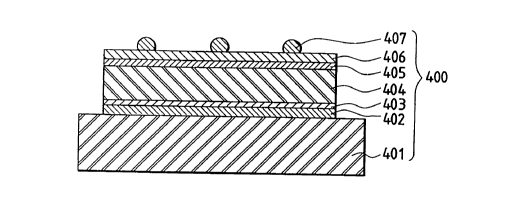
Shown in Figs. 4A to 4C is a typical cross section
of an amorphous silicone based solar cell, which
receives light from the surface opposite the substrate.
In this figure, 401 is the substrate, 402 is the lower
electrode, 403, 413 and 423 are the n-type
semiconductor layers, 404, 414 and 424 are i-type
semiconductor layers, 405, 415 and 425 are p-type
semiconductor layers, 406 is the upper electrode
consisting of a transparent conductive film and 407 is
the grid electrode where a collector electrode is used.
Fig. 5 shows a cross section of a monocrystal
silicone solar cell. 501 is the semiconductor layer
consisting of the silicone wafer substrate, 502 is the
semiconductor layer which forms a pn junction with the
semiconductor layer 501, 503 is the rear face
electrode, 504 is the collecting electrode and 505 is
the low reflection coating.
Fig. 6 shows the cross section of a
polycrystalline silicone solar cell, 601 is a
semiconductor layer consisting of a silicon wafer
substrate, 602 is a semiconductor layer which forms a
pn junction with semiconductor layer 601, 603 is the
rear face electrode, 604 is the collecting electrode
and 605 is the low reflection coating.
_ 47 _ 21 61 ~32
Fig. 7 shows the cross section of a thin film
polycrystalline silicon solar cell, 701 is the
substrate, 702 is the polycrystalized semiconductor
layer, 703 is the semiconductor layer which forms a pn
junction with semiconductor layer 702, 704 is the rear
face electrode, 705 is the collecting electrode and 706
is the low reflection coating.
Figs. 8A and 8B show the solar cells shown in
Figs. 4A to 4C through 7, from the light entry side.
801 is the substrate, 802 is the positive electrode,
803 is the negative electrode and 804 is the collecting
electrode.
The structure of the "photovoltaic element" in
this invention, is desirable to consist of, for
example, a semiconductor layer which contributes to
electricity generation, a transparent conductive layer
installed on the light entry side of the semiconductor
layer, a collecting electrode consisting of the metal
wire and conductive adhesive on the transparent
electrode and a rear face electrode installed on the
side opposite of light entry of the semiconductor
layer.
The semiconductor layer is required to have a
structure which possesses semiconductor junctions, such
as pn junction, pin junction or Schottky splicing, etc.
Materials suitable for this purpose are, for example,
semiconductors in the group IV, such as crystalline
2 1 6 1 932
silicon, polycrystalline silicone and amorphous
silicon, semiconductors in the group II-VI, such as Cds
and CdTe, or semiconductors in the group III-V, such as
GaAs.
In the photovoltaic element of this invention, the
collecting electrode is positioned on the light entry
side of the semiconductor layer, positioned in a
parallel configuration, with appropriate spacing. The
electrode in this invention is particularly suitable
for the formation of photovoltaic elements with large
areas. For example, when producing a 30 cm x 30 cm
photovoltaic element, collecting electrodes can be
formed by placing electrodes, consisting of metal wires
30 cm in length and conductive adhesive, on the
semiconductor layer at specified intervals.
Furthermore, for the purpose of sending electric
currents from the collecting electrode to one terminal,
a bus bar electrode of relatively large capacity is to
be formed.
The rear face electrode of the photovoltaic
element stated in this invention is one that is
installed on the rear face of the semiconductor layer,
the metal of which is formed, for example, by screen
printing or deposition. The type of metal used, should
be chosen from one that offers good ohmic contact with
the semiconductor.
When the semiconductor layer is made of a thin
- 49 -
2l 61 ~32
film consisting of monocrystal semiconductors
containing amorphous silicon, microcrystal silicon or
polycrystalline silicon based substances, it will need
a subsidiary substrate. Both insulative and conductive
substrates may be used for the subsidiary substrate.
Substrates of metals, such as stainless steel or
aluminum are suitable for use and these also function
as the rear face electrode. When insulative
substrates, such as glass, polymer and ceramics, etc.
are used, metals such as chrome, aluminum or silver are
to be depositioned to create the rear face electrode.
The lower electrode 402 is an electrode on one side to
retrieve the power generated in the semiconductor
layers 403, 404, 405, 413, 414, 415, 423, 424 and 425,
and is required to possess a work function that will
create an ohmic contact with semiconductor layer 403.
Materials used are, for example, metals or alloys, and
transparent conductive oxides (TCO), such as Al, Ag,
Pt, Au, Ni, Ti, Mo, W, Fe, V, Cr, Cu, nichrome, SnO2,
In203j ZnO or ITO, etc. It is desirable that the surface
of the lower electrode is smooth, but it may be
textured if it is a cause of irregular reflection of
light. Also, if substrate 401 is conductive, there is
no need for a lower electrode 402. The lower electrode
may be formed with well-known methods, such as plating,
depositioning or spattering.
Not only are single structure with n-layer 403,
- 2161932
i-layer 404 and p-layer 405 as one set suitable for the
amorphous silicone semiconductor layer, but so are
double or triple structure consisting of two or three
sets of pin or pn junctions. Materials such as a-Si,
a-SiGe and a-Sic, or the so called group IV and group
IV alloy-type amorphous semiconductors, are suitable in
particular, for the semiconductor material used for the
i-layers 404, 414 and 424. Methods such as
depositioning, spattering, high-frequency plasma CVD,
microplasma CVC, ECR, heat CVD, and LPCVD methods, for
example, can be used for the film formation of the
amorphous semiconductor layer if desired. Transparent
conductive film 406 is required when the sheet
resistance is high, such as is the case with amorphous
silicone. And because it is positioned on the light
entry side, it is required to be transparent.
Materials such as SnO2, In203, ZnO, CdO, CdSNO4 and ITO,
for example are suitable for the transparent conductive
film 406.
As for monocrystal silicone solar cell 500 and
polycrystalline silicon solar cell 600, a subsidiary
substrate is not installed and the monocrystal wafer
501 and polycrystalline wafer 601 act as the
substrates. The monocrystal wafer 501 is made by
cutting, etc. an Si ingot which is pulled up with the
CZ method. The polycrystalline wafer 601 is formed by
cutting an Si ingot obtained with the cast method or by
- 51 -
2161932
obtaining a polycrystal in sheet form using the ribbon
method. For example, the vapor phase diffusion method
using POC 13, the coat diffusion method using TiO2,
SiO2 or P205, or the ion placing method which dopes it
directly in ions is used to make semiconductor layers
502 and 602. The rear face electrodes 503 and 603 are
made by forming metal films with deposition or
spattering, or by screen printing of silver paste. The
low reflection coating 504 and 604 are formed to
prevent the loss of efficiency, caused by light
reflecting off of the solar cell surface. Suitable
materials are, for example, SiO2, Ta20s and Nb20s.
The thin film polycrystal 700 is formed by growing
Si polycrystal thin film 702 on substrate 701 made of
alumina or graphite, etc. And in some cases, a
particle diameter enlargement process is conducted,
after which this is used as a substrate once again,
onto which the base layer is formed, on top of which
the surface layer 703 is formed using the epitaxial
growth process. Low cost substrates, such as metal Si
may be used for substrate 701.
The second electrode consisting of the collecting
electrode of this invention is positioned on the light
entry side of the semiconductor layer. It is desirable
that they be positioned in appropriate intervals, so
that the sum of the loss caused by the electric
resistance of current collecting and shadow loss is
- 52 -
2 1 6 1 932
minimam. For example, if sheet resistance is
approximately 100 ohms/~, the desired intervals of the
collecting electrodes would be about 5 mm. Also,
optimization by narrowing pitch for thin diameter wires
and widening pitch for thicker diameter wires will
offer optimum efficiency.
The electrode in this invention is particularly
suitable for the formation of solar cells with large
areas. For example, when producing a 30 cm x 30 cm
solar cell, collecting electrodes can be formed by
placing electrodes of this invention, on the
semiconductor layer at specified intervals.
Furthermore, for the purpose of sending electric
currents from the collecting electrode to one terminal,
a tab may be positioned as the collector.
A solar cell produced in this manner is
encapsulated using a well-known process, for better
weather resistance and to maintain its mechanical
strength, and is modularized for outdoor use. In
specific terms, with regard to the materials used for
encapsulation, EVA (ethylene vinyl acetate), etc. is
suitable for the adhesive layer. It is also acceptable
to impregnate EVA in clay glass, etc. to improve
mechanical strength. In addition, a fluoride resin is
laminated as a surface protectant to improve moisture
and scratch resistance. Suitable materials are for
example, a polymer of tetrafluoroethylene (TFE), a
- 53 - 21 61 932
-
copolymer (ETFE) of tetrafluoroethylene and ethylene,
polyvinyl fluoride and polychloro fluoroethylene
(CTFE), etc.. It is also acceptable to improve their
weather resistance by adding ultraviolet ray absorbers
to the resin. As for the method of laminating these
resins with the solar cell substrate, heating and
compression in a vacuum, using a commercially available
device, such as vacuum laminator, for example, can be
used.
Fig. 9 is a typical cross section showing an
example of the photovoltaic element. In Fig. 9, 901 is
the subsidiary substrate, 902 is the rear face
electrode, 903 is the p-type semiconductor layer, 904
is the i-type semiconductor layer, 905 is the n-type
semiconductor layer, 906 is the light receiving plane
electrode and 907 is the collecting electrode.
Fig. 10 is a type diagram of a photovoltaic
element module 100, using a "collecting electrode
coated with conductive adhesive consisting of two
layers (hereinafter abbreviated as: two-layer coated
collecting electrode)" of this invention. In Fig. 10,
1001 is the photovoltaic element substrate, 1002 is the
positive electrode, 1003 is the negative electrode and
1004 is the two-layer coated collecting electrode of
this invention. Photovoltaic element substrate 1001 is
made by forming films of p, i and n semiconductor and
transparent conductive layers on the stainless steel
2161932
- 54 -
substrate, using the CVD or spattering process. The
positive electrode 1002 is an electrode which is used
to retrieve the current collected by the collecting
electrode and materials suitable for this are, for
example, copper or silver plated copper which offer
good conductance. The negative electrode 1003 is an
electrode which is used to retrieve current from the
stainless steel substrate and the material suitable for
this would also be copper. The two-layer coated
collecting electrode 1004 has the function of
collecting the current generated by the photovoltaic
element substrate. The two-layer coated collecting
electrode 1004 is mechanically and electrically
connected to the photovoltaic element substrate and the
positive electrode by means of the thermocompression
process.
In terms of the method by which the metal wire is
positioned as the collecting electrode on the
photovoltaic element; for example, when more than one
wires are to be positioned on the surface of the
photovoltaic element surface; optimum efficiency can be
obtained with optimization procedures, namely narrowing
the pitch for thin wires and widening the pitch for
thicker wires.
As for the method of adhesion, the outer most
layer of the collecting electrode must not be cured
during application on the wire and only be dried of the
2161932
- 55 -
solvent. And heated when adhering to achieve adhesion
and curing.
(Production method)
One method of production of the photovoltaic
element of this invention is, for example the
production method of photovoltaic cells described
below.
It is desirable to adhere the collecting electrode
to the semiconductor or the transparent electrode of
the light entry side with heat and/or pressure.
The desirable heating temperature would be the
softening point of the adhesive layer and the
conductive resin of the second layer, which will form
the adhesive layer. It is desirable that only the
adhesive layer and the second layer will be softened to
make the collecting electrode adhere to the solar cell,
without softening the first layer to maintain the
initial film thickness. Also, if block isocyanate is
used as the curing agent for the conductive resin, it
is desirable to apply temperatures exceeding the
dissociation temperature of isocyanate, so that curing
will occur during the adhesion process.
The desirable pressure will be such that the
adhesive layer and said second layer will undergo
moderate deformation, but must also be lower than any
pressure that will destroy the solar cell. In specific
terms, O.lkg to 1.0 kg/cm2 would be suitable for solar
_ - 56 ~ 21 61 932
cells with thin films, such as amorphous silicon.
If the adhesive layer and the second layer, which
will form the adhesive layer, are of the hot-melt type,
the desirable adhesive method would be to soften them
and adhering them to the solar cell. Suitable pressure
may be applied during adhering. If the second layer is
thermoplastic, it will soften with heat. For heat
curing resins, it is acceptable to dry the solvent,
leaving the resins uncured during the application
process to the wire for them to be heat cured during
adhesion.
Also, the collecting electrode of this invention
and the photovoltaic elements using the collecting
electrode and their production method are entirely
applicable to the photovoltaic elements other than the
solar cell.
(Curing agents to be included in the conductive
adhesive)
One of the problems of production is that, in
order to produce coated wire electrodes off-line and to
facilitate storage until the formation of electrodes,
it is difficult to control accelerated hardening of the
resins, after the resin has been coated and dried on
the metal wire. By using block isocyanate as the
curing agent, only the solvent contained in the resin
is dried during and after the coating drying process,
and by heating it at a constant temperature, the block
2 1 6 1 932
- 57 -
-
agent dissociates, allowing active isocyanate radicals
to react with the resin to achieve hardening. In other
words, whereas it has been very difficult to control
accelerated hardening with other curing agents, such
problems are solved by using block isocyanate as the
curing agent.
(The glass transition point of the conductive
adhesives)
Another production related problem was, that it is
convenient for handling if the metal wires are wound to
a bobbin, etc. after the resin has been coated,
however, the tackiness of the coated wires themselves
made it difficult to unwind them from the bobbin and in
some cases where tackiness was strong, the coating
would peel off. This occurs when the glass transition
point of the coating layer resin is low. By using
resins with glass transition points of over 0 C, the
effects of tackiness reduction can-be felt, but better
results are obtained when the glass transition
temperature is over 100 C. Also, by mixing polymers
with different glass transition points, it becomes
possible to form coating layers with superior
properties in terms of flexibility, adhesion and
reduced tackiness. Preferable combinations are
urethane resin and phenoxy resin, etc.
(The average particle diameter of primary particle of
conductive particles)
2161932
- 58 -
To obtain stably a coating layer with uniform film
thickness and good conductivity, the dispersibility of
conductive particles into resin becomes important as
well as the selection of high polymer. Although the
diameter of a conductive particle should be formed
smaller than the thickness of conductive coating layer,
too small diameter increases resistance at the surface
of particles where they contact each other, making it
impossible to obtain the desired resistivity. When the
conductive particles are dispersed into the resin,
agglomerated particles exist; such as primary particles
which are systematically agglomerated crystallites,
secondary particles which consist of primary particles
agglomerating with particles' surface charge or van der
Waals force or with other force. If the dispersibility
is poor, agglomerated particles of a high order would
exist to cause not only ununiform film thickness but
also unstable conductivity. This invention has solved
the problem by making the average diameter of primary
particles of conductive particles in the coating layer
bigger than 0.02 um and smaller than 15 ,um, the sizes
which prevent formation of agglomerated particles of a
higher order. As the method to measure particles'
agglomerating state in dispersion and particles'
diameter (generally called 'grading'), there are the
laser diffraction method, the light-particle
correlation method, the light scattering method etc.
21~1932
- 59 -
The suitable conductive particles for the coating
layer are graphite, In203, SnO2, TiOz, ITO, ZnO, and
oxide semiconductor materials made from the materials
by adding suitable dopants. The conductive particles
and the polymer are mixed at a suitable ratio to obtain
the desired resistivity. Although increased conductive
particles reduce resistivity, they decrease the ratio
of resin resulting in poor stability as coating film.
Therefore, a suitable ratio should be properly selected
considering what kind of high polymer and conductive
particles will be used and what physical property value
is desired for the film. Going into detail, around 5
volume percent to 95 volume percent of conductive
particles give good resistivity. When the conductive
particles and polymer are mixed, ordinary dispersing
methods, such as a three-roll-mill or a paint shaker
etc., can be used. During or after the dispersion, the
conductive paint can be diluted with a suitable solvent
to adjust viscosity.
(The thickness of coating layer composed of conductive
adhesive)
A problem during and after the formation of
electrodes on a photovoltaic element is forming of
pinholes which causes leakage current to defective
parts reducing the characteristics of the photovoltaic
element. However, this problem is solved by forming
coated layers precisely and forming coating layers with
2161932
- 60 -
-
sufficient thickness. The thickness of the coating
layer varies with the diameter of the metal wire or
characteristics desired. For example, when the metal
wire is 100 ,um in diameter, to have sufficient function
as a barrier layer against leakage current, at the same
time not to cause extreme shadow loss, the suitable
thickness is between 1 ,um and 30 ~m. Another problem
is, while forming of electrodes, metal wires touch the
solar cell substrate to cause shunt. The solution to
this problem is to form more than 2 of coating layers,
and to harden completely the innermost layer of the
coating layer while coating. In this way, metal wires
are prevented from direct contact with the solar cell
substrate during the compression process. The
problems, such as migration etc., which occur when a
photovoltaic element is used outdoors, can be solved by
separating functions into layers; by preparing more
than 2 layers of coating layers to share the functions
such as current collecting, shunt prevention, migration
prevention, electrode fixing, etc.
Fig. 2A shows the sectional plan of an electrode
with conductive coating layer on. Fig. 2C shows the
sectional plan of the part where the electrode is fixed
on a photovoltaic element substrate through the coating
layer. In Fig. 2A and Fig. 2C, 201 is the metal wire,
202 is the primary coating layer which is directly
coated on the metal wire, 203 is the secondary coating
21 61 932
layer which forms the outermost layer, 205 is the
coating layer (the whole) composed of conductive
adhesive, and 206 is the photovoltaic element
substrate. Coating of conductive coating layers is
desired to be made cocentrically. As the method to
coat the conductive resin on the metal wire, the
ordinary spreading method of insulating coating film,
the method used for enameled wire, can be suitably
used. Going into detail, the conductive resin is
diluted with a solvent to obtain suitable viscosity,
then coats the metal wire with a roll coater, etc. The
coated wire is passed through the dice to form a
desired thickness, and is put in a furnace for drying
the solvent and heat curing.
(Components of photovoltaic element)
In the following part, the components of
photovoltaic element will be explained according to the
invention, using Fig. 4A, Fig. 4C, and Fig. 13. Fig.
4A shows an amorphous silicon solar cell which has
single cell structure with the light incidence on the
other side of the substrate. Fig. 4C shows an
amorphous silicon solar cell which has a triple
structure of the solar cell in Fig. 4A. Fig. 13 shows
the solar cells when looked at from the side of light
incoming side shown in Figs. 4A and 4C. Grid
electrodes of about 30 cm long are seen formed.
Although no illustrations are shown, it goes
21 61 932
- 62 -
without saying that the composition according to the
invention's idea can be applied to amorphous silicon
solar cells which are accumulated on a transparent
insulated substrate, and also to monocrystalline and
thin-film polycrystalline solar cells.
In Fig. 4A, 401 shows the subsidiary substrate,
402 shows the lower electrode, 403, 404, and 405
respectively show the semiconductor layer which form
pin-junction, 406 shows the upper electrode of
transparent conductive film, and 407 shows the grid
electrode using collecting electrode.
In Fig. 4C, 403, 404, and 405 show the
semiconductor layers which form the first pin-junction,
413, 414, and 415 show the semiconductor layers which
form the second pin-junction, 423, 424, and 425 show
the semiconductor layers which form the third
pin-junction.
In Fig. 13, 1301 shows the metal tab, 1302 shows
the output port of anode, and 1303 shows the output
port of cathode.
(Substrate)
The substrate 401 according to the invention is a
membrane which mechanically supports semiconductor
layers 403, 404 and 405 which are a thin film solar
cell such as non-crystaline silicone. It is also used
as an electrode in some cases. The substrate 401 has a
required heat resistance to the heat temperature for
21 61 932
- 63 -
forming film of semiconductor layers 403, 404 and 405.
However, both the one having the electroconductive
property and the one having an electro insulating
property can be used. As electroconductive material,
such metals as Fe, Ni, Cr, Al, Mo, Au, Nb, Ta, V, Ti,
Pt, Pb and Ti are used; these alloys, for example,
brass and stainless steel thin plate and its complex,
carbon sheet and zinc plated steel plate are among
those that can be used. As electro insulating
material, film or sheet of heat resistant resin such as
polyester, polyethylene, polycarbonate, cellulose
acetate, polypropylene, polyvinylchloride,
polyvinylidenechloride, polystyrene, polyamide,
polyimide and epoxy resin are used. Or the compound
with the resin and glass fiber, carbon fiber, boron
fiber, metal fiber are among those also cited. And on
the surface of the thin metallic plate and resin sheet,
a coating treatment with foreign material metal thin
film and/or insulating thin film of SiO2, Si3N4, Al2O3,
AlN, etc., is carried out by a sputtering, vapor
deposition and plating method. Glass and ceramic are
also cited.
(Lower electrode)
According to the invention, the lower electrode
402 is one electrode to take out the electric power
generated at semiconductor layers 403, 404, and 405.
It is required to have such a work function as to form
2161932
_ - 64 -
an ohmic contact to the semiconductor layer 403. As
its materials, for example, Al, Ag, Pt, Au, Ni, Ti, Mo,
W, Fe, V, Cr, Cu, stainless steel, brass, nichrome,
SnO2, In203, ZnO, ITO, etc. are used as simple metallic
substances or as their alloys or as transparent
conductive oxides (TCO), etc. Although the surface of
the lower electrode 402 is desirable to be smooth, the
surface can be textured to cause diffused reflection of
light. When the substrate 401 is conductive, the lower
electrode 402 is not necessarily to be prepared.
The methods to prepare the lower electrode are
plating, deposition, spattering etc. As the methods to
prepare the upper electrode, there are the
ohmic-resistance heating deposition method, the
electron beam heating deposition method, the spattering
method, the spraying method etc. to choose the desired.
(Semiconductor layer)
According to the invention, the named
semiconductor layers are amorphous silicon,
polycrystalline silicon, monocrystalline silicon, etc..
In an amorphous silicon solar cell, the semiconductor
materials to compose i-layer 404 are; a-Si:H, a-Si:F,
a-Si:H:F, a-SiGe:H, a-SiGe:F, a-SiGe:H:F, a-SiC:H,
a-SiC:F, a-SiC:H:F, etc. The named are, what is
called, IV group and the IV group's alloy-amorphous
semiconductor. The semiconductor materials to compose
p-layer 405 or n-layer 403 are obtained from the
21 61 q32
semiconductor materials for the i-layer 404 by doping
valence electron control agent. As the materials for
valence electron control agent to obtain p-type
semiconductor, the compounds of elements in group III
of the periodic table are used. Elements in group III
are B, Al, Ga, and In. As the valence electron control
agent to obtain n-type semiconductor, the compounds of
elements in group V of the periodic table are used.
The elements in group V are P, N, As, and Sb.
The methods to form films of amorphous silicon
semiconductor layers can be chosen whatever desired
from the well known methods such as the deposition
method, the spattering method, the RF plasma CVD
method, the microwave plasma CVD method, the ECR
method, the thermal CVD method, the LPCVD method, etc.
Industrially, the RF plasma CVD method is favorably
used, in which the material gas is decomposed with RF
plasma and accumulated on the substrate. However, the
RF plasma CVD method has problems such as the low yield
in the material gas decomposition (about 10 ~) and the
slow accumulating speed (about 0.1 nm/sec. to 1
nm/sec.). The microwave plasma CVD method is
attracting attention as an improved method for these
problems. As the reactor to do the film formation,
well known devices, such as the Batch reactor or a
continuous film formation device, etc., can be used
whatever desired. The invented solar cell can also be
2161932
- 66 -
used for, what is called, tandem cell or triple cell,
in which more than two semiconductor splices are
laminated in order to obtain better spectral
sensitivity and higher voltage.
(Upper electrode)
According to the invention, the upper electrode
406 is the electrode to take out electromotive force
generated at the semiconductor layers 403, 404; and
405. It makes the pair to the lower electrode 402.
The upper electrode 406 is necessary for semiconductors
with high sheet resistivity, such as amorphous silicon.
Because crystalline solar cells have low sheet
resistivity, they do not necessarily need the upper
electrode. The upper electrode 406 is positioned on
the light incoming side and it needs to be transparent,
and it is also called the transparent electrode. The
upper electrode 406 is desirable to have more than 85 %
of transmissivity for effective absorption of light
from the sun and daylight fluorescent lamps etc. into
semiconductor layers. Electrically, the upper
electrode 406 is desirable to have a sheet resistivity
value of less than 100 Q/D to let the electric current
generated with light flow horizontally to the
semiconductor layers. Materials with these
characteristics are the metal oxides of SnO2, In203,
ZnO, CdO, CdSnO4, ITO, etc.
(Grid electrode)
2161932
- 67 -
The grid electrode 407 consists of the metal wire
201, as shown in Fig. 2A, and the conductive coating
layer 205. The conductive coating layer 205 needs to
have resistivity value which is low enough not to
reduce the efficiency of photovoltaic element and at
the same time high enough to prevent shunt. That is,
it does not act as resistance to the electric current
generated by solar cells, but works as resistance to
prevent serious leakage when any defect is around. The
suitable resistivity value for the conductive coating
layer 205 depends on the design of the grid, and on the
photovoltaic element's electric current value and the
scale of defect at its operating point. The desirable
resistivity value is 0.1 - 100 Qcm. When shunt occurs
in this range, the value becomes sufficient resistance,
and at the same time, this value is almost negligible
to the electric current generated at the photovoltaic
element. The grld electrode 407 is positioned on the
light incoming surface side of the photovoltaic element
400 (shown in Fig. 4A). As the grid's arrangement, the
parallel arrangement with suitable intervals is
recommendable. The invented collecting electrodes are
particularly suitable for forming a solar cell with
large area. For example, when solar cell of 30 cm2 is
built, all needed is to install the invented collecting
electrodes of 30 cm long parallel on the semiconductor
layer with prescribed intervals. Furthermore, because
21 61 932
- 68 -
the electrode is composed to reduce the current leakage
caused by shunt or leaks, it is suitable for amorphous
silicon solar cells. However, such composition is, of
course, applicable to other types of solar cells than
amorphous silicon type; to the solar cell of
monocrystalline, polycrystalline, or of other
semiconductors than silicon, or of Shottky splicing
type.
(Tab)
According to the invention, the tab 501 is the
collector which collects the flowing current at the
grid electrode 407 to one end. As the materials for
the collector, metals like Cu, Ag, Pt, and alloys of
these metals are usable. The desirable shapes are
sheets, tapes, or foils to be glued with adhesive
agents.
(The method to form the collecting electrode on the
photovoltaic element)
According to the invention, as "the method to form
the collecting electrode on the photovoltaic element",
the following method is illustrated as how to build
solar cells.
The collecting electrodes are desirable to be
glued on the light incoming side of the semiconductor
layer or on the surface of the transparent conductive
film, using heat, pressure, or both.
The favorable heating temperature is to higher
- 69 - 21 61 932
-
than the softening point of the outermost coating
layer, which is to become the glueing layer, and of the
high polymer which forms the coating layer. When the
conductive resin's hardening agent is composed of block
isocyanates, it is desirable to keep the temperature
higher than the block isocyanate's dissociation
temperature, then let the resin cause heat curing while
glueing process.
The favorable pressure should be high enough to
suitably transform the glueing layer, the outermost
layer of the coating layer, but should be lower than
the pressure which keeps the solar cell without
damaging. Going into detail, for example, for a
film-type solar cell, such as amorphous silicon, a
pressure of 0.1 kg/cm2 to 1.0 kg/cm2 will be suitable.
As the glueing method, when the glueing layer, the
outermost layer of the coating layer, is hot-melt-type,
it is desirable to be glued to the solar cell by
softening with heat. While glueing, a suitable
pressure can be applied.
(Encapsulation)
The solar cell made by the abovementioned method
is modularized by well-known encapsulation in order to
improve weather resistance and mechanical strength. As
encapsulation material, adhesive layer is concerned,
EVA (ethylene vinyl acetate) is favorably used from the
point of adhesive property to solar cell, weather
2161932
- 70 -
-
resistance and buffer effect. In order to improve
further moisture resistance and anti scratching
property, a fluorine resin is laminated as a surface
protecting layer. For example, 4 fluoro ethylene
copolymer TFE (Du Pont TEFLON), copolymer of 4
fluoroethylene and ethylene ETFE (Du Pont TEFZEL),
polyvinyl fluoride (Du Pont TEDLER), polyvinyl fluoride
(Du Pont TEDLER), polychlorofluoroethylene CTFEC Daikin
Industries Neoflon) are cited. Weather resistance can
also be improved by adding well-known UV absorber.
As the method for encapsulation, for example, it
is desirable to use well known devices such as the
vacuum laminater, for thermocompression bonding of the
solar cell substrate and the resin film in a vacuum.
(Embodiment)
The following is the detailed and embodied
explanation of this invention's "the collecting
electrode, the photovoltaic element with the collecting
electrodes, and their building process". However, this
invention shall not be limited by these embodiments.
Firstly, in Embodiments 1 - 40 and Examples for
Comparisons 1 - 2, a detailed discussion is given on
"the case when conductive adhesive is composed of
conductive particles and high polymer".
Secondary, in Embodiments 41 - 46 and Examples for
Comparisons 3 - 4, a detailed discussion is given on
"the case when the coating layer is composed of at
2161932
_~ - 71 -
least more than 2 layers, and at least the conductive
adhesive, which forms the outermost layer of the
coating layers, is composed of not yet hardened but
heat curing high polymer".
Furthermore, in Embodiments 47 - 55 and Examples
for Comparisons 5 - 6, a detailed discussion is given
on "the case when the conductive adhesive contains
coupling agent".
Concerning Embodiments 1 - 40 and Examples for
Comparisons 1 - 2, the following information is
collected and shown in Tables 9 - 16; the formative
conditions of the collecting electrode, the solar cell
structure, and the characteristic evaluation results of
solar cells.
(Embodiment 1)
In this embodiment, an explanation is given on the
case when a collecting electrode is composed of Cu
wire, carbon black, and urethane.
As Fig. lA shows, the collecting electrode 100 of
this invention was formed as follows. As the metal
wire 101, copper wire of 100 ,um in diameter was used.
The carbon paste, to form conductive adhesive for
the coating layer 102, was prepared as follows. First,
a mixed solvent of ethyl acetate 2.5 g and IPA 2.5 g
was placed in a shake bottle for dispersion. Next,
22.0 g of urethane resin, the main ingredient, was
added into the shake bottle, and all was mixed
2161932
- 72 -
thoroughly with the ball mill. The number average
molecular weight of urethane resin was 3000. Then,
1.1 g of block isocyanate, as a hardening agent, and
10 g of glass beads, for dispersion, were added to the
solution. Then, as conductive particles, 2.5 g of
carbon black of 0.05 ,um in average primary particle
diameter was added to the solution.
The shake bottle containing the materials was
placed in a paint shaker, of Toyo Seiki Co., for 10
hours for dispersion. Then glass beads for dispersion
were removed from the prepared paste. The average
particle diameter of the paste was measured to be about
1 ~m. The results of using the beads mill instead of a
paint shaker were almost the same.
The paste was hardened at 160C for 30 minutes,
the standard hardening condition of the hardening
agent. Its volume resistivity was measured to be 0.6
Qcm to prove being low enough.
The void ratio of the paste was measured by a
mercury Polosimeter to be 0.01 ml/g. Then, carbon
black was removed from the paste and only resin was
hardened to form a sheet. Its gel ratio was measured
to be approximately 100 %.
The coating layer 102 was formed as follows, using
a vertical wire-coating machine 300 shown in Fig. 3.
First, the delivery reel 301 was set with a reel
which is wound with metal wire 307. Next, the metal
2161q32
- 73 -
wire was stretched toward the take-up reel 310. Then,
the paste was poured into the coater.
The coating speed was 40 m/min, and the residence
time was 2 seconds. The drying furnace 306 was set at
120C. The coating was done 5 times. The dice, the
one for enamel coating, were used in a variety of
diameters, from 110 ,um to 200 ,um in order. Under this
condition, the paste was preserved, with solvent
evaporated and in unhardened state. The thickness of
the coating layer 102 was 20 ,um on average. Variations
in the film thickness after c`oating were within +0.5 ,um
per 100 m.
As an embodiment of this invention, an amorphous
solar cell 400 was built. It had the layer composition
shown in Fig. 4C and pin-junction-type triple structure
with grid electrodes of 30 cm long.
First, an SUS 430 BA substrate 401 was thoroughly
degreased and washed, then was placed in a DC
spattering device (not illustrated) to accumulate 450
nm of Ag followed by 1000 nm of ZnO. Thus the lower
electrode 402 was formed. The substrate was taken out
and placed in a microwave plasma CVD film formation
device (not illustrated) to form in order of silicon
layer as the n-layer 403, silicon-germanium layer as
the i-layer 404, and silicon layer as the p-layer 405.
Thus the bottom layer was formed. Then, in the same
way, the middle layer was formed in order of silicon
216193~
- 74 -
layer as the n-layer 413, silicon-germanium layer as
the i-layer 414, and silicon layer as the p-layer 415.
The top layer of the silicon layer was formed in order
of the n-layer 423, the i-layer 424, and the p-layer.
Thus, the semiconductor layer was accumulated. Then,
it was placed in the spattering device (not
illustrated) to form 70 nm of IT0 film, the transparent
conductive film 406, which also has low reflectance
function. Then, the solar cell substrate 401 was
trimmed into the size of 30 x 30 cm with an effective
area of 900 cm2 by removing unnecessary part of
transparent conductive film, using etching paste, whose
main ingredient is ferric chloride, and a printer on
the market.
Then, out of the effective area, the anode 802 and
the cathode 803, both of hard copper, were prepared.
As the collecting electrode 805, the coated wire lO0
was stretched between the both anode 802 at 6 mm
intervals and to be within the effective area, then was
fixed with an ultraviolet-ray hardening adhesive.
The fixed said coating wire 100 was bonded by
thermocompression, using a heating device (not
illustrated), to form the collecting electrode 804 on
the cell surface of the solar cell substrate 401 and on
the anode 802. Thus, a triple-cell of 30 x 30 cm,
shown in Fig. 8A, was built. The heating condition
was; at 200C, for 45 seconds, and at the pressure of 1
2161932
- 75 -
kg/cm2.
The encapsulation of this sample was done as
follows. On the top and bottom of the solar cell
substrate 801, plane glass and EVA were laminated, and
fluorine-contained resin film ETFE (Tefzel of Du Pont)
was laminated further on the top and bottom of it.
Then, the substrate was placed in a vacuum laminater
and laminated at 150C for 60 minutes.
In the same method, 50 solar cell modules were
built.
The initial characteristics of the obtained sample
were measured as follows. First, the voltage/current
characteristics were measured in the dark state. The
shunt resistivity was measured at the slope near the
home position to be 200 kQcm2 to 500 kQcm2, favorable
results. Next, the solar cell characteristics were
measured, using pseudo solar light source (hereafter
called simulator) with quantity of light of 100 mW/cm2
by the AM 1.5 global sunlight spectrum. The obtained
conversion efficiency was 9.6 % + 0.02 %, showing
favorable characteristics with little variations. The
series resistivity was 32.0 Qcm2 on average, also a
favorable value. The yield rate of normal I-V curve
was favorable 94 %.
The reliability test was given to these samples in
conformity with the Japanese Industrial Standards C
8917; the environmental testing method for crystalline
2161932
- 76 -
-
solar cell modules, and the hygrothermal cycle test
A - 2 provided by the endurance testing method.
The samples were placed in a thermo-hygrostat,
which can control temperatures and humidity, and
repeated 20 times of cycle tests varied between -40C
and +85C (with relative humidity 85 %). Then, the
samples, which completed the cycle test, were measured
their solar cell characteristics in the same way as the
initial characteristics were, using the simulator. Its
conversion efficiency was lower 2 % on average than the
initial value, showing no occurrence of meaningful
deterioration.
The results of this embodiment show that a solar
cell, with collecting electrodes of the metal wire
coated with the invented conductive adhesive, has
favorable characteristics and high reliability.
(Example for Comparison)
In this example, as a conventional example, an
explanation is given on the case when the collecting
electrode consists of Cu wire with fluorine-contained
resin paste containing carbon.
For comparison, the conventional collecting
electrode 100 was built in the same way as in
Embodiment 1, in Fig. lA, with the following
exceptions.
The paste, used for the coating layer 102 of the
collecting electrode 100 in Fig. lA, was a
2161932
fluorine-contained resin paste (Electrodag +502 SS of
Acheson Colloid), similar to the one mentioned in the
U. S. Patent No. 4,260,429.
The wire was coated in the same way as in
Embodiment 1. The thickness of the coating layer 102
was 20 ,um on average, and the deflection of film
thickness in 100 meter long was over +1.0 ,um after
coating.
The paste was hardened at 120C for 5 minutes, the
standard hardening condition for the hardening agent.
The volume resistivity was measured to be 0.1 Qcm2, a
low enough value. The hole volume of this conductive
adhesive was 0.05 ml/g. Then, like in Embodiment 1, 50
solar cell modules were built, using this wire as
collection electrodes.
The initial characteristics of the obtained sample
were measured in the similar method to Embodiment 1.
First, the shunt resistivity was measured to be
4 kQcmZ - 300 kQcm2, showing a wide variation. Next,
the conversion efficiency was obtained to be 9.0 % +1.2
%, varying widely. The series resistivity of normal
1 - 1 V curve was obtained to be 32.1 Qcm2 on average, a
favorable value. The initial yield rate of normal
I - V curve was as low as 64 %.
The reliability test was done to this sample
similarly to Embodiment 1. The tested sample was
measured its solar cell characteristics with the
2161932
- 78 -
simulator similarly to the initial characteristics.
The result was on average 11 % lower than the initial
conversion efficiency, showing the occurrence of
meaningful deterioration. The series resistivity was
measured to have risen to 62 Qcm2 on average. This
indicated that the rise of the series resistivity
caused the deterioration of the conversion efficiency.
It is supposed that the outside humidity entered
into the device to raise the interfacial resistivity in
the contacting part of the paste in the adhesive
interface of coating layer and transparent conductive
film surface.
This result showed that the solar cell using the
invented collecting electrodes have a good initial
yield rate and favorable reliability.
(Embodiment 2)
In this example, an explanation is given on the
case when the collecting electrode consists of Cu wire,
IT0, and butyral.
In this case, the same process was used to build
collecting electrodes as in Embodiment 1, except that ,
for the invented collecting electrode 100 according to
the invention shown in Fig. lA, butyral resin (Slec BL
- S of Sekisui Chemical Co., Ltd.) was used as the main
ingredient high polymer to form conductive adhesive,
and that IT0 powder (HYX of Sumitomo Metal Mining Co.,
Ltd.) of 0.05 ,um in the average primary particle
2161932
- 79 -
diameter was used as conductive particles.
The above-described paste was hardened at the
temperature of 160 C for thirty minutes which were the
standard hardening condition of the above-described
hardener and then was measured in its volume
resistivity, and it was verified that its volume
resistivity was low enough because the measured value
was 1.2 Q cm2. Further, transmittance of light was
measured using a spectroscope and its transmittance was
satisfactory because the measured value was 90% per 400
nm. The volume of a hole of this conductive adhesive
agent was 0.02 ml/g and the ratio of gel was 20%. The
average molecular weight of polymeric resin was fifty
thousand.
Wire was coated as the first embodiment to form a
collecting electrode 100. Fifty solar battery modules
were produced using the collecting electrode 100 by the
same method as that in the first embodiment.
The initial characteristics of the obtained sample
were measured by the same method as that in the first
embodiment and satisfactory characteristics could be
obtained because its conversion efficiency was 9.7% +
0.05%, its shunt resistance was 250 to 300 kQ cm2, its
series resistance was 32.5 Q cm2 on average. The yield
rate of samples of which I-V curve was normal was
satisfactory because it was 94%.
The reliability test of these samples was
2161932
- 80 -
performed by the same method as that in the first
embodiment. Next, the solar battery characteristics of
the samples after the test was finished were measured
using a simulator as in measurement of initial values,
and its measured conversion efficiency was lower 2~ on
average than the initial conversion efficiency,
however, no significant deterioration occurred.
The result of this embodiment shows a solar
battery using a collecting electrode according to the
invention has excellent characteristics and high
reliability.
(Embodiment 3)
Referring to this embodiment, the case that a
collecting electrode comprises Ag wire, urethane and
SnO2 will be described.
In this embodiment, a collecting electrode 100
according to the invention shown in Fig. lA is produced
as the first embodiment except that a metallic wire 101
is formed by silver, and SnO2 powder manufactured by
Mitsui Mining and Smelting Co., Ltd. of which average
primary particle diameter is 0.2 ,um is used as a
conductive particle forming a coated layer 102.
The above-described paste was hardened at the
temperature of 160 C for thirty minutes which were the
standard hardening condition of the above-described
hardener and then, was measured in its volume
resistivity, and it was verified that its volume
2161932
- 81 -
resistivity was low enough because the measured value
was 1.0 Q cm2. Wire was coated as the first embodiment
to form a collecting electrode 100. Fifty solar
battery modules were produced using the collecting
electrode 100 by the same method as that in the first
embodiment.
The initial characteristics of the obtained sample
were measured by the same method as that in the first
embodiment and satisfactory characteristics could be
obtained because its conversion efficiency was 9.1% +
0.06%, its shunt resistance was 250 to 400 kQ cm2, its
series resistance was 32.9 Q cm2 on average. The yield
rate of samples of which I-V curve was normal was
satisfactory because it was 92%.
The reliability test of these samples was
performed by the same method as that in the first
embodiment. Next, the solar battery characteristics of
the samples after the test was finished were measured
using a simulator as in measurement of initial values,
and the conversion efficiency was lower 2.5% on average
than the initial conversion efficiency, however, no
significant deterioration occurred.
The result of this embodiment shows a solar
battery using a collecting electrode according to the
invention has excellent characteristics and high
reliability.
(Embodiment 4)
2161~32
- 82 -
Referring to this embodiment, the case that a
collecting electrode comprises Au wire, polyamide and
In203 will be described.
In this embodiment, a collecting electrode 100
according to the invention shown in Fig. lA is produced
as the first embodiment except that a metallic wire 101
is formed by gold, polyamide resin manufactured by
Mitsubishi Chemical Industries Ltd. is used as
polymeric resin which mainly constitutes paste forming
a coated layer 102, and In203 manufactured by Sumitomo
Metal Mining Co., Ltd. of which average primary
particle diameter is 0.05 ,um is used as a conductive
particle.
The above-described paste was hardened at the
temperature of 160 C for thirty minutes which were the
standard hardening condition of the above-described
hardener and then, was measured in its volume
resistivity, and it was verified that its volume
resistivity was low enough because the measured value
was 1.5 Q cm2. The volume of a hole of this conductive
adhesive was 0.04 l/g and average molecular weight of
polymeric resin was ten thousand.
Wire was coated as the first embodiment to form a
collecting electrode 100. Fifty solar battery modules
were produced using the collecting electrode 100 by the
same method as that in the first embodiment.
The initial characteristics of the obtained sample
2161932
- 83 -
were measured by the same method as that in the first
embodiment and satisfactory characteristics could be
obtained because its conversion efficiency was 9.2% +
0.01%, its shunt resistance was 400 to 500 kQ cm2, its
series resistance was 32.3 n cm2 on average. The yield
rate of samples of which I-V curve was normal was
satisfactory because it was 90%.
The reliability test of these samples was
performed by the same method as that in the first
embodiment. Next, the solar battery characteristics of
the samples after the test was finished were measured
using a simulator as in measurement of initial values,
and the conversion efficiency was lower 2% on average
than the initial conversion efficiency, however, no
significant deterioration occurred.
The result of this embodiment shows a solar
battery using a collecting electrode according to the
invention has excellent characteristics and high
reliability.
(Embodiment 5)
Referring to this embodiment, the case that a
collecting electrode comprises Cu wire, silver clad,
urethane and carbon black will be described.
In this embodiment, a collecting electrode 100
according to the invention shown in Fig. lB is produced
as the first embodiment except that a silver-clad
copper wire 100 ,um in diameter produced by forming a
- 84 _ 2 1 6 1 932
silver-clad metal layer 103 2 ,um thick on a copper wire
101 to enhance adhesion and electrical connection with
a conductive adhesive is used.
Paste for forming a conductive adhesive for a
coated layer 102 is produced as follows:
First, mixed solution comprising ethyl acetate 2.5 g
and IPA 2.5 g as a solvent is put in a shaker for
dispersion. Next, urethane resin 22.0 g which is main
material is added in the above-described shaker and is
sufficiently stirred with a ball mill. Next, as a
hardener, block isocyanate 1.1 g and glass beads for
dispersion 10 g are added in the above-described
solution. Next, carbon black 2.5 g of which average
primary particle diameter is 0.05 ,um as a conductive
particle is added in the above-described solution.
The shaker in which the above-described materials
were put is dispersed with a paint shaker manufactured
by Toyo Precision Mechanical Equipment for ten hours.
Then, the glass beads for dispersion are removed from
produced paste. The average particle diameter of the
paste was measured and the measured value was
approximately 1 ~m. The similar result was also
obtained if a bead mill was used in place of a paint
shaker.
The above-described paste was hardened at the
temperature of 160 C for thirty minutes which were the
standard hardening condition of the above-described
2161932
- 85 -
hardener and then, was measured in its volume
resistivity, and it was verified that its volume
resistivity was low enough because the measured value
was 0.6 Q cm2.
Next, a coated layer 403 is formed using a
vertical-type wire coating machine 400 shown in Fig. 4
as described below.
A layer 102 was coated on a silver-clad layer 103
as the first embodiment to form a collecting electrode
100. Fifty solar battery modules were produced using
the collecting electrode 100 by the same method as that
in the first embodiment.
The initial characteristics of the obtained sample
were measured by the same method as that in the first
embodiment and satisfactory characteristics could be
obtained because its conversion efficiency was 9.7% +
0.03~, its shunt resistance was 300 to 400 kQ cm2, its
series resistance was 31.5 Q cm2 on average. The yield
rate of samples of which I-V curve was normal was
satisfactory because it was 90%.
The reliability test of these samples was
performed by the same method as that in the first
embodiment. Next, the solar battery characteristics of
the samples after the test was finished were measured
using a simulator as in measurement of initial values,
and the conversion efficiency was lower 1.5~ on average
than the initial conversion efficiency, however, no
2161932
- 86 -
significant deterioration occurred.
The result of this embodiment shows a solar
battery using a collecting electrode according to the
invention has excellent characteristics and high
reliability.
(Embodiment 6)
Referring to this embodiment, the case that a
collecting electrode comprises Cu wire, silver clad,
phenoxy and ZnO will be described.
In this embodiment, a collecting electrode 100
according to the invention shown in Fig. lB is produced
as the fifth embodiment except that phenoxy resin
manufactured by PKHH Tomoe Industries is used as
polymeric resin which mainly constitutes paste forming
a coated layer 102 and ZnO powder manufactured by
Mitsui Mining and Smelting Co. Ltd. of which average
primary particle diameter is 0.1 ,um is used as a
conductive particle.
The above-described paste was hardened at the
temperature of 160 C for thirty minutes which were the
standard hardening condition of the above-described
hardener and then, was measured in its volume
resistivity, and it was verified that its volume
resistivity was low enough because the measured value
was 1.3 Q cm2. The volume of a hole of this conductive
adhesive was 0.01 ml/g and the ratio of gel was 100%.
The average molecular weight of polymeric resin was
2161932
- 87 -
-
twenty-five thousand.
Wire was coated as the fifth embodiment to form a
collecting electrode 100. Fifty solar battery modules
were produced using the collecting electrode 100 by the
same method as that in the first embodiment.
The initial characteristics of the obtained sample
were measured by the same method as that in the first
embodiment and satisfactory characteristics could be
obtained because its conversion efficiency was 9.6% +
0.02%, its shunt resistance was 310 to 390 kQ cm2, its
series resistance was 32.4 Q cm2 on average. The yield
rate of samples of which I-V curve was normal was
satisfactory because it was 94%.
The reliability test of these samples was
performed by the same method as that in the first
embodiment. Next, the solar battery characteristics of
the samples after the test was finished were measured
using a simulator as in measurement of initial values,
and the conversion efficiency was lower 2% on average
than the initial conversion efficiency, however, no
significant deterioration occurred.
The result of this embodiment shows a solar
battery using a collecting electrode according to the
invention has excellent characteristics and high
reliability.
(Embodiment 7)
Referring to this embodiment, the case that a
2161932
- 88 -
collecting electrode comprises Cu wire, silver clad,
phenoxy and ZnO + Al will be described.
In this embodiment, a collecting electrode 100
according to the invention shown in Fig. lB is produced
as the fifth embodiment except that ZnO powder produced
by adding aluminum to ZnO as dopant so as to lower
contact resistance of a conductive particle is used.
The above-described paste was hardened at the
temperature of 160 C for thirty minutes which were the
standard hardening condition of the above-described
hardener and then, was measured in its volume
resistivity, and it was verified that its volume
resistivity was low enough because the measured value
was 0.9 Q cm2.
Wire was coated as the fifth embodiment to form a
collecting electrode 100. Fifty solar battery modules
were produced using the collecting electrode 100 by the
same method as that in the first embodiment.
The initial characteristics of the obtained sample
were measured by the same method as that in the first
embodiment and satisfactory characteristics could be
obtained because its conversion efficiency was 9.6% _
0.09%, its shunt resistance was 400 to 500 kQ cm2, its
series resistance was 31.5 Q cm2 on average. The yield
rate of samples of which I-V curve was normal was
satisfactory because it was 92%.
The reliability test of these samples was
2 1 G ~ ~32
- 89 -
-
performed by the same method as that in the first
embodiment. Next, the solar battery characteristics of
the samples after the test was finished were measured
using a simulator as in measurement of initial values,
and the conversion efficiency was lower 2~ on average
than the initial conversion efficiency, however, no
significant deterioration occurred.
The result of this embodiment shows a solar
battery using a collecting electrode according to the
invention has excellent characteristics and high
reliability.
(Embodiment 8)
Referring to this embodiment, the case that a
collecting electrode comprises Cu wire, silver plating,
urethane and TiO2 will be described.
In this embodiment, a collecting electrode 100
according to the invention shown in Fig. lB is produced
as the fifth embodiment except that a metallic layer
103 on a copper wire 101 is changed from silver clad
according to the fifth embodiment to silver plating and
TiO2 manufactured by Ishihara Sangyo Kaisha of which
average primary particle diameter is 0.2 ,um is used as
a conductive particle.
The above-described paste was hardened at the
temperature of 160 C for thirty minutes which were the
standard hardening condition of the above-described
hardener and then, was measured in its volume
2161932
-- 90 --
-
resistivity, and it was verified that its volume
resistivity was low enough because the measured value
was 1.1 Q cmZ. Wire was coated as the fifth embodiment
to form a collecting electrode 100.
Fifty solar battery modules were produced using
the collecting electrode 100 by the same method as that
in the first embodiment.
The initial characteristics of the obtained sample
were measured by the same method as that in the first
embodiment and satisfactory characteristics could be
obtained because its conversion efficiency was 9.5% +
0.01%, its shunt resistance was 400 to 500 kQ cm2, its
series resistance was 31.6 Q cm2 on average. The yield
rate of samples of which I-V curve was normal was
satisfactory because it was 92%.
The reliability test of these samples was
performed by the same method as that in the first
embodiment. Next, the solar battery characteristics of
the samples after the test was finished were measured
using a simulator as in measurement of initial values,
and the conversion efficiency was lower 2.3% on average
than the initial conversion efficiency, however, no
significant deterioration occurred.
The result of this embodiment shows a solar
battery using a collecting electrode according to the
invention has excellent characteristics and high
reliability.
2161~32
- 91 -
(Embodiment 9)
Referring to this embodiment, the case that a
collecting electrode comprises Cu wire, tin plating,
polyamide and graphite will be described.
In this embodiment, a collecting electrode 100
according to the invention shown in Fig. lB is produced
as the fifth embodiment except that a metallic layer
103 on a copper wire 101 is changed from silver clad
according to the fifth embodiment to tin plating, and
polyamide imide resin manufactured by Mitsubishi
Chemical Industries Ltd. is used as polymeric resin
which mainly constitutes paste and a conductive
particle is changed to graphite manufactured by Tokai
Carbon.
The above-described paste was hardened at the
temperature of 180 C for thirty minutes which were the
standard hardening condition of the above-described
hardener and then, was measured in its volume
resistivity, and it was verified that its volume
resistivity was low enough because the measured value
was 2.0 Q cm2. The volume of a hole of this conductive
adhesive was 0.01 ml/g and the average molecular weight
of polymeric resin was twenty-five thousand.
Wire was coated as the fifth embodiment to form a
collecting electrode 100. Fifty solar battery modules
were produced using the collecting electrode 100 by the
same method as that in the first embodiment.
2161932
- 92 -
-
The initial characteristics of the obtained sample
were measured by the same method as that in the first
embodiment and satisfactory characteristics could be
obtained because its conversion efficiency was 9.3% +
0.09%, its shunt resistance was 400 to 500 kQ cm2, its
series resistance was 33.6 Q cm2 on average. The yield
rate of samples of which I-V curve was normal was
satisfactory because it was 94%.
The reliability test of these samples was
performed by the same method as that in the first
embodiment. Next, the solar battery characteristics of
the samples after the test was finished were measured
using a simulator as in measurement of initial values,
and the conversion efficiency was lower 2.9% on average
than the initial conversion efficiency, however, no
significant deterioration occurred.
The result of this embodiment shows a solar
battery using a collecting electrode according to the
invention has excellent characteristics and high
reliability.
(Embodiment 10)
Referring to this embodiment, the case that a
collecting electrode comprises Cu wire, silver paste,
urethane and carbon black will be described.
In this embodiment, a collecting electrode 100
according to the invention shown in Fig. lB is produced
as the fifth embodiment except that a metallic layer
216~932
- 93 -
103 on a copper wire 101 is changed from silver clad
according to the fifth embodiment to silver paste, 5007
manufactured by Du Pont.
For paste used for the above-described metallic
layer 103, paste in which a silver particle is
dispersed in epoxy resin is used.
The above-described paste was hardened at the
temperature of 150 C for thirty minutes which were the
standard hardening condition of the above-described
hardener and then, was measured in its volume
resistivity, and it was verified that its volume
resistivity was low enough because the measured value
was 5 x 10⁻⁵ Q cm2.
Next, a metallic layer 302 comprising the above-
described silver paste which is coated on a Cu wiresequentially from the innermost layer by the same
method as that in the first embodiment is constituted
as follows:
First, a reel on which a Cu wire 302 is wound is
set on a delivery reel 301 and the above-described Cu
wire is stretched to a take-up reel 310. Next, the
above-described silver paste 5007 is injected into a
coater.
The take-up speed of Cu wire shall be 40 m/min.,
the hardening time 2 sec., the temperature of a drying
furnace 200 C and the diameter of the used die for
enamel coating 160 ,um. The above-described conditions
2161q32
_ - 94 -
on which paste 5007 applied on wire is hardened are
determined based upon the result of experiments. The
thickness of formed metallic layer 103 was 5 um on
average and fluctuation of the thickness of film when
wire 100 m long was coated was within +0.2 ,um.
Next, a carbon paste-coated layer 102 comprising
urethane resin was formed by the same method as that in
the fifth embodiment.
The thickness of the coated layer 102 was 20 ,um on
average and fluctuation of the thickness of film when a
wire 100 m long was coated was within +1 ,um.
Next, fifty solar battery modules using this wire
as a collecting electrode which were constituted as in
the first embodiment and shown in Fig. 8A were
produced.
The initial characteristics of the obtained sample
were measured by the same method as that in the first
embodiment. First, the shunt resistance was checked
and a satisfactory value could be obtained because the
measured value was 150 to 200 kQ cm2. Next, the
characteristics of the above-described solar battery
were measured, and it was verified that such solar
battery had satisfactory characteristics and such
characteristics varied little because its conversion
efficiency was 9.2% + 0.05% and its series resistance
was 31.8 Q cm2 on average. The yield rate of samples of
which I-V curve was normal was satisfactory because it
2161932
- 95 -
was 88%.
The reliability test of these samples was
performed by the same method as that in the first
embodiment. Next, the solar battery characteristics of
the samples after the test was finished were measured
using a simulator as in measurement of initial values,
and the conversion efficiency was lower 2.1% on average
than the initial conversion efficiency, however, no
significant deterioration occurred.
Next, a test in which low illuminance of light was
irradiated to such solar battery module under the
environment where the temperature was +85 C and the
relative humidity was 85% so as to check possibility of
migration of silver because silver is used for a
collecting electrode was continued for lO0 hours.
Next, the shunt resistance of such sample after
the above-described test was finished was measured by
the same method as that in the first embodiment, as a
result, the measured value was 130 to 160 kQ cm2, and no
significant deterioration occurred.
The result of this embodiment shows a solar
battery using a metallic wire on which a conductive
adhesive is coated according to the invention as a
collecting electrode has excellent characteristics and
high reliability.
(Embodiment ll)
In this embodiment, an amorphous solar battery 400
2161932
_ - 96 -
is produced according to the following procedure by the
same method as that in the first embodiment except that
it is constituted as a single type which is constituted
only by a Si layer shown in Fig. 4A and radio-frequency
(RF) plasma CVD is used for forming a semiconductor
layer.
First, SUS430BA substrate 401 sufficiently
degreased and cleaned is put in a DC sputtering device
not shown, Ag is deposited until the film is 400 nm
thick, then ZnO is deposited until the film is 400 nm
thick so as to form the lower electrode 402. The
substrate is taken out of the sputtering device and is
put in a RF plasma CVD film forming system not shown,
and a silicon semiconductor layer is formed in the
order of n layer 403, i-layer 404 and p-layer 405.
Then, the substrate is put in a resistance heating
deposition system not shown and In2O3 film is formed as
transparent conductive film 506 provided with a
function also with anti-reflection effect. Next, fifty
solar battery modules were produced using the above-
described collecting electrode 100 by the same method
as that in the first embodiment. At this time, the
above-described coated wire 100 was used at intervals
of 5.5 mm.
The initial characteristics of the obtained sample
were measured by the same method as that in the first
embodiment and satisfactory characteristics could be
_ 97 2 1 6 1 q32
-
obtained because its conversion efficiency was 5.2% +
0.05%, its shunt resistance was 150 to 320 kn cm2, its
series resistance was 9.5 Q cm2 on average. The yield
rate of samples of which I-V curve was normal was
satisfactory because it was 90%.
The reliability test of these samples was
performed by the same method as that in the first
embodiment. Next, the solar battery characteristics of
the samples after the test was finished were measured
using a simulator as in measurement of initial values,
and the conversion efficiency was lower 2.4% on average
than the initial conversion efficiency, however, no
significant deterioration occurred.
The result of this embodiment shows a solar
battery using a collecting electrode according to the
invention has excellent characteristics and high
reliability.
(Embodiment 12)
In this embodiment, an amorphous solar battery 400
is produced according to the following procedure by the
same method as that in the first embodiment except that
it is constituted as a double type which is constituted
by two Si layers shown in Fig. 4B and RF plasma CVD is
used for forming a semiconductor layer.
First, SUS430BA substrate 401 sufficiently
degreased and cleaned is put in a DC sputtering device
not shown, Ag is deposited until the film is 400 nm
- 98 - 21 61 932
-
thick, then ZnO is deposited until the film is 400 nm
thick so as to form the lower electrode 402. The
substrate is taken out of the sputtering device and is
put in a RF plasma CVD film forming system not shown,
and the bottom layer of a silicon layer is formed in
the order of n layer 403, i-layer 404 and p-layer 405.
Next, similarly, the top layer of a silicon layer is
sequentially formed in the order of n layer 413,
i-layer 414 and p-layer 415, and as a result, a silicon
semiconductor layer is deposited. Then, the substrate
is put in a resistance heating deposition system not
shown and In203 film is formed as transparent conductive
film 406 provided with a function also with anti-
reflection effect.
Next, fifty solar battery modules were
produced using the above-described collecting electrode
100 by the same method as that in the first embodiment.
At this time, the above-described coated wire 100 was
used at intervals of 5.5 mm.
The initial characteristics of the obtained sample
were measured by the same method as that in the first
embodiment and satisfactory characteristics could be
obtained because its conversion efficiency was 7.5% +
0.01%, its shunt resistance was 400 to 500 kQ cm2, its
series resistance was 23.1 Q cm2 on average. The yield
rate of samples of which I-V curve was normal was
satisfactory because it was 94%.
2161932
99
The reliability test of these samples was
performed by the same method as that in the first
embodiment. Next, the solar battery characteristics of
the samples after the test was finished were measured
using a simulator as in measurement of initial values,
and the conversion efficiency was lower 1.9% on average
than the initial conversion efficiency, however, no
significant deterioration occurred.
The result of this embodiment shows a solar
battery using a collecting electrode according to the
invention has excellent characteristics and high
reliability.
(Embodiment 13)
In this embodiment, an amorphous solar battery 400
is produced according to the following procedure by the
same method as that in the first embodiment except that
it is constituted as a double type which is constituted
by Si and SiGe layers shown in Fig. 6, RF plasma CVD is
used for forming a semiconductor layer, and a silicon
germanium semiconductor layer is used for i-layer of
the bottom layer.
First, SUS430BA substrate 401 sufficiently
degreased and cleaned is put in a DC sputtering device
not shown, Ag is deposited until the film is 400 nm
thick, then ZnO is deposited until the film is 400 nm
thick so as to form the lower electrode 402. The
substrate is taken out of the sputtering device and is
loo 2 1 6 1 932
put in a microwave plasma CVD film forming system not
shown, and the bottom layer is formed in the order of a
silicon layer for n layer 403, a silicon germanium
layer for i-layer 404 and a silicon layer for p-layer
405. Next, similarly, the top layer of a silicon layer
is sequentially formed in the order of n layer 413,
i-layer 414 and p-layer 415, and as a result, a silicon
semiconductor layer is deposited. Then, the substrate
is put in a resistance heating deposition system not
shown and In203 film is formed as transparent conductive
film 406 provided with a function also with anti-
reflection effect.
Next, fifty solar battery modules were
produced using the above-described collecting electrode
100 by the same method as that in the first embodiment.
At this time, the above-described coated wire 100 was
used at intervals of 5.5 mm.
The initial characteristics of the obtained sample
were measured by the same method as that in the first
embodiment and satisfactory characteristics could be
obtained because its conversion efficiency was 7.7% +
0.02%, its shunt resistance was 400 to 500 kQ cm2, its
series resistance was 20 Q cm2 on average. The yield
rate of samples of which I-V curve was normal was
satisfactory because it was 92%.
The reliability test of these samples was
performed by the same method as that in the first
-lol- 2161932
embodiment. Next, the solar battery characteristics of
the samples after the test was finished were measured
using a simulator as in measurement of initial values,
and the conversion efficiency was lower 2.0% on average
than the initial conversion efficiency, however, no
significant deterioration occurred.
The result of this embodiment shows a solar
battery using a collecting electrode according to the
invention has excellent characteristics and high
reliability.
(Embodiment 14)
In this embodiment, an amorphous solar battery 400
is produced according to the following procedure by the
same method as that in the first embodiment except that
it is constituted as a triple type which is constituted
by SiC, Si and SiGe layers shown in Fig. 4C, RF plasma
CVD is used for forming a semiconductor layer, and a
silicon germanium semiconductor layer is used for
i-layer of the bottom layer.
First, SUS430BA substrate 401 sufficiently
degreased and cleaned is put in a DC sputtering device
not shown, Ag is deposited until the film is 400 nm
thick, then ZnO is deposited until the film is 400 nm
thick so as to form the lower electrode 402. The
substrate is taken out of the sputtering device and is
put in a microwave plasma CVD film forming system not
shown, and the bottom layer is formed in the order of a
~ 61 ~2
- 102 -
silicon layer for n layer 403, a silicon germanium
layer for i-layer 404 and a silicon layer for p-layer
405. Next, similarly, the middle layer of a silicon
layer is sequentially formed in the order of n layer
413, i-layer 414 and p-layer 415, further the top layer
is formed in the order of a silicon layer for n layer
423, a silicon-C layer for i-layer 404 and a silicon
layer for p-layer 405, and as a result, a semiconductor
layer is deposited. Then, the substrate is put in a
resistance heating deposition system not shown and In203
film is formed as transparent conductive film 406
provided with a function also with anti-reflection
effect.
Next, fifty solar battery modules were
produced using the above-described collecting electrode
lO0 by the same method as that in the first embodiment.
The initial characteristics of the obtained sample
were measured by the same method as that in the first
embodiment and satisfactory characteristics could be
obtained because its conversion efficiency was 9.5% +
0.06%, its shunt resistance was 260 to 330 kQ cmZ, its
series resistance was 33.7 Q cm2 on average. The yield
rate of samples of which I-V curve was normal was
satisfactory because it was 92%.
The reliability test of these samples was
performed by the same method as that in the first
embodiment. Next, the solar battery characteristics of
2161~32
- 103 -
the samples after the test was finished were measured
using a simulator as in measurement of initial values,
and the conversion efficiency was lower 2.4% on average
than the initial conversion efficiency, however, no
significant deterioration occurred.
The result of this embodiment shows a solar
battery using a collecting electrode according to the
invention has excellent characteristics and high
reliability.
(Embodiment 15)
In this embodiment, a monocrystalline solar
battery 500 is produced according to the following
procedure by the same method as that in the first
embodiment except that it is constituted by a
monocrystalline solar battery (monocrystalline Si)
shown in Fig. 5.
First, a silicon monocrystal of which valence
electron is controlled by Czochralski process so that
it is p type is produced, the monocrystal is sliced,
and a silicon wafer 500 approximately 300 ,um thick is
produced. Further, a n+-type layer 501 is formed in a
diffusion process by applying P205 on the above-
described wafer. Next, silver paste is printed on the
rear side of p-layer 500 by a screen printing machine
not shown, heated and burnt, and as a result, the lower
electrode 502 is formed. Next, the above-described
collecting electrode 100 used in the first embodiment
2161932
_ - 104 -
is formed on n~-type layer 501 on the side of light
irradiated face by the above-described method. Then,
SiO2 film 504 is formed as anti-reflection film by a
sputtering process. Next, fifty solar battery modules
shown in Fig. 8B by the same method as that in the
first embodiment were produced. At this time, the
above-described coated wire 100 was used at intervals
of 8.5 mm.
The initial characteristics of the obtained sample
were measured by the same method as that in the first
embodiment and satisfactory characteristics could be
obtained because its conversion efficiency was 15.8% +
0.09%, its shunt resistance was 500 to 760 kQ cm2, its
series resistance was 2.8 Q cm2 on average. The yield
rate of samples of which I-V curve was normal was
satisfactory because it was 98%.
The reliability test of these samples was
performed by the same method as that in the first
embodiment. Next, the solar battery characteristics of
the samples after the test was finished were measured
using a simulator as in measurement of initial values,
and the conversion efficiency was lower 1.9~ on average
than the initial conversion efficiency, however, no
significant deterioration occurred.
The result of this embodiment shows a solar
battery using a collecting electrode according to the
invention has excellent characteristics and high
2 1 61 932
- 105 -
reliability.
(Embodiment 16)
In this embodiment, a polycrystalline solar
battery 600 is produced according to the following
procedure by the same method as that in the first
embodiment except that it is constituted by a
polycrystalline solar battery (polycrystalline Si)
shown in Fig. 6.
First, a polycrystalline ingot is produced by a
casting process, the polycrystal is sliced, and n+-type
layer 601 is formed on the obtained polycrystalline
silicon wafer 600 in a diffusion process by applying
P205 on the above-described wafer. Next, silver paste
is printed on the rear side of p-layer 600 by a screen
printing machine not shown, heated and burnt, and as a
result, the lower electrode 602 is formed. Next, the
above-described collecting electrode 100 used in the
first embodiment is formed on n+-type layer 601 on the
side of light irradiated face by the above-described
method. Then, SiO2 film 604 is formed as anti-
reflection film by a sputtering process. Next, fifty
solar battery modules shown in Fig. 8B by the same
method as that in the first embodiment were produced.
At this time, the above-described coated wire 100 was
used at intervals of 8 mm.
The initial characteristics of the obtained sample
were measured by the same method as that in the first
2161~32
- 106 -
embodiment and satisfactory characteristics could be
obtained because its conversion efficiency was 13.8% +
0.01%, its shunt resistance was 450 to 650 kQ cm2, its
series resistance was 2.6 Q cm2 on average. The yield
rate of samples of which I-V curve was normal was
satisfactory because it was 94%.
The reliability test of these samples was
performed by the same method as that in the first
embodiment. Next, the solar battery characteristics of
the samples after the test was finished were measured
using a simulator as in measurement of initial values,
and the conversion efficiency was lower 2% on average
than the initial conversion efficiency, however, no
significant deterioration occurred.
The result of this embodiment shows a solar
battery using a collecting electrode according to the
invention has excellent characteristics and high
reliability.
(Embodiment 17)
In this embodiment, a thin-film polycrystalline
solar battery 600 is produced according to the
following procedure by the same method as that in the
first embodiment except that it is constituted by a
thin-film polycrystalline solar battery (thin-film
polycrystalline Si) shown in Fig. 7.
First, a metallic Si substrate 701 sufficiently
degreased and cleaned is put in a microwave plasma CVD
21 bl 932
- 107 -
film forming system not shown so as to form n layer
702. Next, this substrate is put in a heating furnace
not shown so as to polycrystallize n layer 702. Then,
the substrate is put in a microwave plasma CVD film
forming system not shown so as to form p-layer 703.
Further, the substrate is put in a sputtering device
not shown and IT0 film is formed as transparent
conductive film 704 provided with a function also with
anti-reflection effect. Next, a collecting electrode
705 is formed on the above-described transparent
conductive film 704 by the same method as that in the
first embodiment and fifty solar battery modules shown
in Fig. 8B were produced.
The initial characteristics of the obtained sample
were measured by the same method as that in the first
embodiment and satisfactory characteristics could be
obtained because its conversion efficiency was 12.5% +
0.01%, its shunt resistance was 400 to 510 kQ cm2, its
series resistance was 20 n cm2 on average. The yield
rate of samples of which I-V curve was normal was
satisfactory because it was 92%.
The reliability test of these samples was
performed by the same method as that in the first
embodiment. Next, the solar battery characteristics of
the samples after the test was finished were measured
using a simulator as in measurement of initial values,
and the conversion efficiency was lower 2.1~ on average
- 108 - 2 1 6 1 9~2
`_
than the initial conversion efficiency, however, no
significant deterioration occurred.
The result of this embodiment shows a solar
battery using a collecting electrode according to the
invention has excellent characteristics and high
reliability.
(Embodiment 18)
This embodiment is different from the first
embodiment in that resistivity of a conductive adhesive
is varied within the range of 0.005 to 200 Q cm. For a
method for varying resistivity of a conductive
adhesive, mixing ratio (in weight) of polymeric resin
and a conductive particle in conductive coating
material was varied to any of 5:95, 10:90, 20:80,
80:20, 90:10, 95:5.
This embodiment is similar to the first embodiment
in other ways.
Ten triple cells shown in Fig. 4C were produced
according to the same procedure as that in the first
embodiment except that these conductive adhesives were
used and similarly evaluated. Table 1 shows the
result.
21 6i -9~2
- 109 -
-
[Table 1]
Resistivity ( n cm) 0.0050.01 1 100 200
Initial status
Transformation
efficiency(%) 8.2 9.6 9.6 9.4 8.5
Series
resistance(Q cm2) 31.4 31.4 31.8 32.3 39.8
Shunt
resistance(kQ cm2) 4.9 25.9 250 320 350
Status after
confidence test
Transformation
efficiency(~) 7.2 9.5 9.5 9.3 7.3
Series
resistance( n cm2) 31.3 31.6 31.9 32.6 50.3
Shunt
resistance(kQ cm2) 2.3 25.9 251 325 350
Table 1 shows that initial shunting can be
controlled by setting the resistivity of a coated layer
102 to 0.01 Q cm or more and more stable conversion
efficiency can be obtained. Table 1 also shows that
series resistance can be reduced by setting the
resistivity to 100 Q cm or less and higher conversion
efficiency can be obtained. Table 1 further shows that
increase of series resistance and lowering of
conversion efficiency after a reliability test can be
reduced and a solar battery using a collecting
electrode according to the invention has high
reliability.
(Embodiment 19)
This embodiment is different from the first
embodiment in that the heating pressure-bonding
temperature of a conductive adhesive is varied in the
2161932
-- 110 --
-
range of 50 to 300 C. For temperature for heating and
pressure-bonding a collecting electrode 100,
measurement was performed at four different temperature
of 100, 160, 200 and 250 C. Used block isocyanate is
similar to that in the first embodiment and its
dissociative temperature is 150 C.
In other ways this embodiment is similar to the
first embodiment.
Ten triple cells shown in Fig. 4 were produced and
similarly evaluated according to the same procedure as
that in the first embodiment except that heating
pressure-bonding temperature was set as their
temperature. Table 2 shows the result.
[Table 2]
Heating pressure- 100 160 200 250
bonding
temperature (C)
Initial status
Transformation
efficiency(%) 6.3 9.0 9.6 9.6
Series
resistance(Q cm2)51.331.4 31.3 31.2
Shunt
resistance(kQ cm2) 57.3 253 352 390
Status after
confidence test
Transformation
efficiency(%) 3.1 8.7 9.6 9.6
Series
resistance(Q cm2)121 36.5 31.3 31.2
Shunt
resistance(kQ cm2) 56.8 254 356 389
2161932
- 111
Table 2 shows that series resistance can be
reduced by setting heating pressure-bonding temperature
to the dissociative temperature or higher of coated
layer resin and higher conversion efficiency can be
obtained. The table 2 also shows increase of series
resistance after a reliability test and lowering of
conversion efficiency can be reduced and a solar
battery using a collecting electrode according to the
invention has high reliability.
(Embodiment 20)
This embodiment is different from the first
embodiment in that the heating pressure-bonding time of
a conductive adhesive is varied in the range of 10 to
60 seconds. For heating pressure-bonding time of a
collecting electrode 100, four different time of 10,
20, 45 and 60 seconds was set. To check the hardening
factor of a conductive adhesive under such a condition,
an amount eluted into a solvent before and after
immersion was measured and as a result, the ratio of
gel was 5%, 15~, 80~ and 100% respectively. Used block
isocyanate is similar to that in the first embodiment
and its dissociative temperature is 150 C.
In other ways this embodiment is similar to the
first embodiment.
Ten triple cells shown in Figs 4A to 4C were
produced and similarly evaluated according to the same
procedure as that in the first embodiment except that
2161932
- 112 -
-
for heating pressure-bonding temperature, the above-
described temperature was set. Table 3 shows the
result.
[Table 3]
Heating contact
bonding 10 20 45 60
time(sec.)
Initial status
Transformation 6.9 8.5 9.5 9.6
efficiency(%)
Series 43.5 36.2 31.4 31.2
resistance(Q cm2)
Shunt 25.1 96.3 265 312
resistance(kQ cm2)
Status after
confidence test
Transformation
efficiency(%) 5.2 8.0 9.5 9.6
Series
resistance(Q cm2) 58.3 40.2 31.5 31.3
Shunt
resistance(kQ cm2) 20.3 96.5 264 315
Table 3 shows that series resistance can be
reduced and higher conversion efficiency can be
obtained by adjusting heating pressure-bonding time and
setting the ratio of gel of coated layer resin to 20%
or more. The table 3 also shows increase of series
resistance after a reliability test and lowering of
conversion efficiency can be reduced and a solar
battery using a collecting electrode according to the
invention has high reliability.
(Embodiment 21)
2161932
- 113 -
-
In this embodiment, the amount of a hardener
applied to a conductive adhesive was measured. The
ratio in weight of urethane resin mainly used for a
coated layer of a collecting electrode 100 and block
isocyanate used for a hardener was changed to 100:1,
50:1, 20:1 and 10:1. At this time, the ratio of gel of
a conductive adhesive was 5%, 15%, 85% and 100%
respectively. Used block isocyanate is similar to that
in the first embodiment and its dissociative
temperature is 150 C.
In other ways this embodiment is similar to the
first embodiment.
Ten triple cells shown in Figs. 4A to 4C were
produced and evaluated according to the same procedure
as that in the first embodiment. Table 4 shows the
result.
- 114 - 2161932
[Table 4]
Ratio of
resin/hardener 100:1 50:1 20:1 10:1
Initial status
Transformation
efficiency(%) 7.8 8.7 9.7 9.6
Series
resistance(Q cm2)39.9 33.8 31.0 31.7
Shunt
resistance(kQ cm2) 15.3 165 369 374
Status after
confidence test
Transformation
efficiency(~) 6.1 8.4 9.7 9.6
Series
resistance(Q cm2)51.2 38.9 31.1 31.9
Shunt
resistance(kQ cm2) 14.2 172 368 372
Table 4 shows that series resistance can be
reduced and higher conversion efficiency can be
obtained by adjusting an amount of a hardener and
setting the ratio of gel of coated layer resin to 20
or more. Table 4 also shows that increase of series
resistance and lowering of conversion efficiency after
a reliability test can be reduced and the table 3 also
shows increase of series resistance after a reliability
test and lowering of conversion efficiency can be
reduced and a solar battery using a collecting
electrode according to the invention has high
reliability.
(Embodiment 22)
Referring to this embodiment, the case that a
- 115 - 21 61 932
collecting electrode comprises Cu wire, carbon black,
urethane will be described.
In this embodiment, a collecting electrode 200
according to the invention shown in Fig. 2A is produced
according to the follow procedure.
For metallic wire 201, a copper wire 100 ,um in
diameter is used.
Carbon paste No. 1 for forming a conductive
adhesive for the first layer 202 is produced according
to the following procedure. First, mixed solution
comprising BCA 2.5 g and xylene 2.5 g as a solvent is
put in a shaker for dispersion. Next, urethane resin
22.0 g which is main material is added in the above-
described shaker and is sufficiently stirred with a
ball mill. Next, as a hardener, block isocyanate 1.1 g
and glass beads for dispersion 10 g are added in the
above-described solution.
Next, carbon black 2.5 g of which average primary
particle diameter is 0.05 ,um as a conductive particle
is added in the above-described solution.
The shaker in which the above-described materials
are put is dispersed with a paint shaker manufactured
by Toyo Precision Mechanical Equipment for ten hours.
Then, the glass beads for dispersion are removed from
produced paste. The average particle diameter of the
paste was measured and the measured value was
approximately 1 ,um. The similar result was also
2161932
- 116 -
obtained if a bead mill was used in place of a paint
shaker.
The above-described paste No. 1 was hardened at
the temperature of 160 C for thirty minutes which were
the standard hardening condition of the above-described
hardener and then, was measured in its volume
resistivity, and it was verified that its volume
resistivity was low enough because the measurea value
was 1.0 Q cm2. The volume of a hole of this conductive
adhesive was 0.01 ml/g and the ratio of gel was 100~.
The average molecular weight of polymeric resin was one
thousand.
Next, carbon paste No. 2 for forming a conductive
adhesive the second layer 203 is produced according to
the following procedure. First, for a solvent,
cyclohexanone 2.5 g is put in a shaker for dispersion.
Next, urethane resin 22.0 g which is main material
and phenoxy resin 2.0 g are added in the above-
described shaker and are sufficiently stirred with a
ball mill. Next, as a hardener, block isocyanate 1.1 g
and glass beads for dispersion 10 g are added in the
above-described solution. Next, carbon black 2.5 g of
which average primary particle diameter is 0.05 ,um as a
conductive particle is added in the above-described
solution. This is dispersed by the same method as that
in the case of paste No. 1.
The above-described paste No. 2 was hardened at
2161932
- 117 -
-
the temperature of 160 C for thirty minutes which were
the standard hardening condition of the above-described
hardener, then the volume resistivity of it was
measured, and it was verified that it was low enough
because the measured value was 0.5 Q cm.
Next, the first layer 202 and the second layer 203
are sequentially formed in the order described above
using a vertical type of wire coater 300 shown in Fig.
3 as follows:
First, a reel on which a metallic wire 307 is
wound is set on a delivery reel 301 and the above-
described metallic wire is stretched to a take-up reel
310. Next, the above-described paste No. 1 is injected
into a coater.
The take-up speed of metallic wire was 40 m/min.,
the residence time was 2 sec., the temperature of a
drying furnace 306 was 350 C and the metallic wire was
coated five times. A die for enamel coating 110 to 200
,um in diameter was sequentially used. Paste No. 1 was
sufficiently hardened on the above-described
conditions, and adhesion and resistance to a solvent of
paste were satisfactory. The thickness of the first
layer 202 was 5 ,um on average and fluctuation of the
thickness of film when wire 100 m long was coated was
within +1 ,um.
Next, the second layer 203 comprising paste No. 2
is formed by the same method as described above except
2161932
- 118 -
-
the described below.
A reel 310 on which the wire on which the above-
described first layer 202 was coated is wound is set on
a delivery reel 301 and the above-described wire is
stretched to a take-up reel 310. Next, the above-
- described carbon paste No. 2 is injected into a coater.
The take-up speed of the wire was 40 m/min., the
drying time was 2 sec., the temperature of a drying
furnace 306 was 120 C and the wire was coated five
times. A die for enamel coating 150 to 200 ,um in
diameter was used. Paste No. 2 applied on the above-
described wire was in a condition not hardened yet in
which its solvent was volatilized. The thickness of
the second layer 203 was 20 ,um on average and
fluctuation of the thickness of film when the wire 100
m long was coated was within +0.5 ,um.
Next, in an embodiment according to the invention,
a pin-junction triple amorphous solar battery 400 with
constitution of layers shown in Figs. 4A to 4C provided
with a grid electrode 30 cm in grid length is produced.
First, SUS430BA substrate 401 sufficiently
degreased and cleaned is put in a DC sputtering device
not shown, Ag is deposited until the film is 400 nm
thick, then ZnO is deposited until the film is 400 nm
thick so as to form the lower electrode 402. The
substrate is taken out of the sputtering device and is
put in a microwave plasma CVD film forming system not
2161932
- 119 -
shown, and the bottom layer is formed in the order of a
silicon layer for n layer 403, a silicon germanium
layer for i-layer 404 and a silicon layer for p-layer
405. Next, similarly, the middle layer is sequentially
formed in the order of a silicon layer for n layer 413,
a silicon germanium layer for i-layer 414 and a silicon
layer for p-layer 415, further the top layer of a
silicon layer is formed in the order of n layer 423, i-
layer 424 and p-layer, and as a result, a semiconductor
layer is deposited. Then, the semiconductor layer is
put in a resistance heating deposition system not shown
and IT0 film is formed as transparent conductive film
506 provided with a function also with anti-reflection
effect. Next, unnecessary transparent conductive film
is removed using etching paste which mainly comprises
ferric chloride and a printing machine on the market so
that the solar battery substrate 401 is 30 x 30 cm in
size and effective area of the cell is 900 cm2.
Next, hard copper positive electrode 802 and
negative electrode 803 are provided outside the
effective area, as a collecting electrode 804 the
above-described coated wire 100 is stretched between
positive electrodes 802 at intervals of 7 mm so that
the wire is contained in the effective area and is
fixed using an ultraviolet hardening adhesive.
Next, the above-described collecting electrode 804
is heated and crimped using a heater not shown so as to
2161932
- 120 -
-
stick the collecting electrode on the cell face of the
solar battery substrate 401 and as a result, a triple
cell 30 x 30 in size shown in Fig. 8A is produced. The
collecting electrode is heated at the temperature of
200 C for 45 seconds under pressure of 1 kg/cm2.
Next, this sample is encapsulated according to the
following procedure. Kroehnkite glass and EVA are
laminated on the upper and rear surfaces of the solar
battery substrate 801, further fluororesin film ETFE is
laminated on the upper and rear surfaces, the substrate
is put in a vacuum laminater and is left at the
temperature of 150 C for an hour for lamination.
Fifty solar battery modules were produced by the
same method.
The initial characteristics of the obtained sample
were measured according to the following procedure.
First, volt-ampere characteristic of the sample in an
off state was measured, its shunt resistance on an
inclination in the vicinity of the origin was 200 to
500 kQ cm2 and it was a satisfactory value. Next, the
solar battery characteristics were measured using a
pseudo solar light source (hereinafter called a
simulator) with a solar spectrum of AM 1.5 global and
quantity of light of 100 mW/cm2, and its conversion
efficiency was satisfactory and there was little
dispersion because the measured value was 9.6% + 0.02%.
Its series resistance was 32.0 Q cm2 on average and
2161932
- 121 -
satisfactory. The yield rate of samples of which I-V
curve was normal was 98~ and satisfactory.
The reliability test of these samples was
performed by the same method as that in the first
embodiment. Next, the solar battery characteristics of
the samples after the test was finished were measured
using a simulator as in measurement of initial values,
and the conversion efficiency was lower 2~ on average
than the initial conversion efficiency, however, no
significant deterioration occurred.
Further, to check moisture resistance and a
leakage factor of these samples, a reliability test was
performed as follows: First, a sample was put in a
constant temperature and humidity oven with a window
lS through which light could be transmitted which could
control temperature and humidity, and was left at the
temperature of +85 C and relative humidity of 85%.
When the temperature and humidity in it was
sufficiently balanced, quantity of light of 100 mW/cm2
with a solar spectrum of AM 1.5 global was irradiated
by a simulator installed outside the window.
Next, the solar battery characteristics of a
sample after a reliability test was finished were
measured using a simulator as in measurement of initial
values and its conversion efficiency was lower 2~ on
average than its initial conversion efficiency,
however, no significant deterioration occurred.
21619~2
- 122 -
The result of this embodiment shows a solar
battery using a metallic wire on which a conductive
adhesive according to the invention is coated as a
collecting electrode has excellent characteristics and
high reliability.
(Comparative Embodiment 2)
Referring to this comparative embodiment, the case
that a collecting electrode comprises Cu wire, Ag and
polyester will be described.
For comparison, paste 5007 including a silver
particle manufactured by Du Pont was coated on wire to
form a collecting electrode 100. The volume of a hole
of this conductive adhesive was 0.1 ml/g. Fifty solar
battery modules were produced using the collecting
electrode 100 by the same method as that in the first
embodiment.
The initial characteristics of the obtained sample
were measured, its conversion efficiency was 7.5% +
1.8%, fluctuation of the values was large. Its shunt
resistance was 1.8 kQ cm2 on average and fluctuation of
the values was large. Its series resistance was 32.0 Q
cm2 on average. The yield rate of samples of which I-V
curve was normal was low because it was 54%.
Samples of which shunt resistance were normal were
selected of these samples and a reliability test of
moisture resistance and leakage was performed by the
same method as that in the twenty-second embodiment.
-l23-2l6l932
-
Next, the solar battery characteristics of a sample
after the test was finished were measured using a
simulator as in measurement of initial values, its
conversion efficiency was lower 20% than its initial
conversion efficiency and its shunt resistance was
smaller than a half of its initial shunt resistance
value.
(Embodiment 23)
Referring to this embodiment, the case that a
collecting electrode comprises Cu wire, carbon black
and epoxy, and carbon black and butyral will be
described.
This embodiment is similar to the twenty-second
embodiment except that epoxy resin manufactured by
Epicoat Petrochemical Shell Epoxy is used as polymeric
resin which mainly constitutes paste No. 1 for forming
a conductive adhesive for a collecting electrode 200
shown in Fig. 2A according to the invention, and
butyryl resin manufactured by Eslec BL-S Sekisui
Chemical is used as polymeric resin which mainly
constitutes paste No. 2.
The volume of a hole of this paste No. 1 was 0.01
ml/g and the ratio of gel was 100%. The average
molecular weight of polymeric resin was one thousand.
The above-described paste No. 1 was hardened at
the temperature of 160 C for thirty minutes which were
the standard hardening condition of the above-described
2161932
- 124 -
hardener, then its volume resistivity was measured, and
it was verified that its volume resistivity was low
enough because the measured value was 2.1 Q cm.
Wire was coated as in the twenty-second embodiment
to form a collecting electrode 200. Fifty solar
battery modules were produced using the collecting
electrode 200 by the same method as that in the twenty-
second embodiment.
The initial characteristics of the obtained sample
were measured by the same method as that in the first
embodiment, its conversion efficiency was 9.4% + 0.06%,
its shunt resistance was 400 to 500 kQ cm2, its series
resistance was 32.2 Q cm2 on average, and satisfactory
characteristics could be obtained. The yield rate of
samples of which I-V curve was normal was 96% and
satisfactory. A reliability test of these samples was
performed as in the twenty-second embodiment. Next,
the solar battery characteristics of a sample after the
test was finished were measured using a simulator as in
measurement of initial values, and its conversion
efficiency was lower 2.6% on average than its initial
conversion efficiency, however, no significant
deterioration occurred.
The result of this embodiment shows a solar
battery using a collecting electrode according to the
invention has satisfactory characteristics and high
reliability.
2161932
- 125 -
_
(Embodiment 24)
Referring to this embodiment, the case that a
collecting electrode comprises Ag wire, carbon black
and urethane, and IT0 and urethane will be described.
This embodiment is similar to the twenty-second
embodiment except that a silver wire is used as a
metallic wire 201 for a collecting electrode 200 shown
in Fig. 2A according to the invention, and IT0 power
manufactured by HYX Sumitomo Metal Mining of which
average primary particle diameter is 0.05 ~m is used as
a conductive particle of paste No. 2 for forming a
conductive adhesive.
The above-described paste No. 2 was hardened at
the temperature of 160 C for thirty minutes which were
the standard hardening condition of the above-described
hardener, then its volume resistivity was measured, and
it was verified that its volume resistivity was low
enough because the measured value was 1.0 Q cm.
Wire was coated as in the twenty-second embodiment
to form a collecting electrode 200. Fifty solar
battery modules were produced using the collecting
electrode 200 by the same method as that in the twenty-
second embodiment.
The initial characteristics of the obtained sample
were measured by the same method as that in the twenty-
second embodiment, its conversion efficiency was 9.5% +
0.07%, its shunt resistance was 300 to 500 kQ cm2, its
2161932
- 126 -
-
series resistance was 32.5 Q cm2 on average, and
satisfactory characteristics could be obtained. The
yield rate of samples of which I-V curve was normal was
94% and satisfactory.
A reliability test of these samples was performed
as in the twenty-second embodiment. Next, the solar
battery characteristics of a sample after the test was
finished were measured using a simulator as in
measurement of initial values, and its conversion
efficiency was lower 2.3~ on average than its initial
conversion efficiency, however, no significant
deterioration occurred.
The result of this embodiment shows a solar
battery using a collecting electrode according to the
invention has satisfactory characteristics and high
reliability.
(Embodiment 25)
Referring to this embodiment, the case that a
collecting electrode comprises Ag wire, graphite and
urethane, and SnO2 and urethane will be described.
This embodiment is similar to the twenty-second
embodiment except that a gold wire is used as a
metallic wire 201 for a collecting electrode 200 shown
in Fig. 2A according to the invention, graphite power
manufactured by Tokai Carbon of which average primary
particle diameter is 0.05 ~um is used as a conductive
particle of paste No.1 for forming a conductive
21~932
- 127 -
adhesive, and SnO2 power manufactured by Mitsui Mining
and Smelting Co., Ltd. of which average primary
particle diameter is 0.2 ,um is used as a conductive
particle of paste No. 2.
The above-described paste No. 1 was hardened at
the temperature of 180 C for thirty minutes which were
the standard hardening condition of the above-described
hardener, then its volume resistivity was measured, and
it was verified that its volume resistivity was low
enough because the measured value was 1.8 Q cm.
The above-described paste No. 2 was hardened at
the temperature of 160 C for thirty minutes which were
the standard hardening condition of the above-described
hardener, then its volume resistivity was measured, and
it was verified that its volume resistivity was low
enough because the measured value was 1.4 Q cm.
Wire was coated as in the first embodiment to form
a collecting electrode 200. Fifty solar battery
modules were produced using the collecting electrode
200 by the same method as that in the twenty-second
embodiment.
The initial characteristics of the obtained sample
were measured by the same method as that in the twenty-
second embodiment, its conversion efficiency was 9.3~ +
0.01~, its shunt resistance was 230 to 420 kQ cm2, its
series resistance was 33.0 Q cm2 on average, and
satisfactory characteristics could be obtained. The
2161932
- 128 -
yield rate of samples of which I-V curve was normal was
96% and satisfactory.
A reliability test of these samples was performed
as in the twenty-second embodiment. Next, the solar
battery characteristics of a sample after the test was
finished were measured using a simulator as in
measurement of initial values, and its converslon
efficiency was lower 2.1% on average than its initial
conversion efficiency, however, no significant
deterioration occurred.
The result of this embodiment shows a solar
battery using a collecting electrode according to the
invention has satisfactory characteristics and high
reliability.
(Embodiment 26)
Referring to this embodiment, the case that a
collecting electrode comprises Cu wire, silver clad,
carbon black and urethane will be described.
This embodiment is similar to the twenty-second
embodiment except that a silver clad copper wire 100 ,um
in diameter produced by forming a silver clad metallic
layer 203 having the thickness of 2 ,um on a copper wire
201 is used for a collecting electrode 200 according to
the invention shown in Fig. 2A so as to enhance
adhesion to a conductive adhesive and conductivity.
Wire was coated as in the first embodiment to form a
collecting electrode 200. Further, fifty solar battery
21 6 1 932
- 129 -
-
modules were produced using the collecting electrode
100 by the same method as that in the twenty-second
embodiment.
The initial characteristics of the obtained sample
were measured by the same method as that in the twenty-
second embodiment, its conversion efficiency was 9.7% +
0.02%, its shunt resistance was 400 to 500 kQ cm2, its
series resistance was 31.8 Q cm2 on average, and
satisfactory characteristics could be obtained. The
yield rate of samples of which I-V curve was normal was
98% and satisfactory.
A reliability test of these samples was performed
as in the twenty-second embodiment. Next, the solar
battery characteristics of a sample after the test was
finished were measured using a simulator as in
measurement of initial values, and its conversion
efficiency was lower 2% on average than its initial
conversion efficiency, however, no significant
deterioration occurred.
The result of this embodiment shows a solar
battery using a collecting electrode according to the
invention has satisfactory characteristics and high
reliability.
(Embodiment 27)
Referring to this embodiment, the case that a
collecting electrode comprises Cu wire, silver clad,
ZnO and urethane, and In2O3 and urethane will be
- 130 _ 21 61 932
described.
This embodiment is similar to the twenty-second
embodiment except that for a collecting electrode 200
according to the invention shown in Fig. 2A, a silver
clad copper wire is used, ZnO power manufactured by
Mitsui Mining and Smelting Co., Ltd. of which average
primary particle diameter is 0.1 ,um is used as a
conductive particle of paste No. 1 for forming a
conductive adhesive, and In203 powder manufactured by
Sumitomo Metal Mining Co., Ltd. of which average
primary particle diameter is 0.05 ~m is used as a
conductive particle of paste No. 2.
The above-described paste No. 1 was hardened at
the temperature of 160 C for thirty minutes which were
the standard hardening condition of the above-described
hardener, then its volume resistivity was measured, and
it was verified that its volume resistivity was low
enough because the measured value was 1.4 Q cm.
The above-described paste No. 2 was hardened at
the temperature of 160 C for thirty minutes which were
the standard hardening condition of the above-described
hardener, then its volume resistivity was measured, and
it was verified that its volume resistivity was low
enough because the measured value was 0.7 Q cm.
Wire was coated as in the twenty-second embodiment
to form a collecting electrode 200. Fifty solar
battery modules were produced using the collecting
2161932
- 131 -
electrode 200 by the same method as that in the twenty-
second embodiment.
The initial characteristics of the obtained sample
were measured by the same method as that in the twenty-
second embodiment, its conversion efficiency was 9.6% +0.03~, its shunt resistance was 320 to 390 kQ cm2, its
series resistance was 32.1 Q cm2 on average, and
satisfactory characteristics could be obtained; The
yield rate of samples of which I-V curve was normal was
96% and satisfactory.
A reliability test of these samples was performed
as in the twenty-second embodiment. Next, the solar
battery characteristics of a sample after the test was
finished were measured using a simulator as in
measurement of initial values, and its conversion
efficiency was lower 2% on average than its initial
conversion efficiency, however, no significant
deterioration occurred.
The result of this embodiment shows a solar
battery using a collecting electrode according to the
invention has satisfactory characteristics and high
reliability.
(Embodiment 28)
Referring to this embodiment, the case that a
collecting electrode comprises Cu wire, silver plating,
carbon black and phenol, and carbon black and polyamide
will be described.
2161~32
- 132 -
This embodiment is similar to the twenty-second
embodiment except that for a collecting electrode 200
according to the invention shown in Fig. 2A, a silver-
plated wire 100 lum in diameter produced by plating
silver clad with silver is used as a metallic layer
203, phenol resin manufactured by Dainippon and
Chemicals, Inc. is used as main material for polymeric
resin of paste No. 1 for forming a conductive adhesive,
and polyamide resin manufactured by Mitsubishi Kasei
Corporation is used as main material for polymeric
resin of paste No. 2. The volume of a hole of this
paste No. 1 was 0.01 ml/g and the ratio of gel was
100%. The average molecular weight of polymeric resin
was one thousand.
The above-described paste No. 1 was hardened at
the temperature of 160 C for thirty minutes which were
the standard hardening condition of the above-described
hardener, then its volume resistivity was measured, and
it was verified that its volume resistivity was low
enough because the measured value was 1.5 Q cm.
The above-described paste No. 2 was hardened at
the temperature of 160 C for thirty minutes which were
the standard hardening condition of the above-described
hardener, then its volume resistivity was measured, and
it was verified that its volume resistivity was low
enough because the measured value was 0.8 Q cm.
Wire was coated as in the first embodiment to form
- 133 _ 2161932
a collecting electrode 200. Fifty solar battery
modules were produced using the collecting electrode
200 by the same method as that in the twenty-second
embodiment.
The initial characteristics of the obtained sample
were measured by the same method as that in the twenty-
second embodiment, its conversion efficiency was 9.3% +
0.01%, its shunt resistance was 400 to 500 kQ cm2, its
series resistance was 32.7 Q cm2 on average, and
satisfactory characteristics could be obtained. The
yield rate of samples of which I-V curve was normal was
96% and satisfactory.
A reliability test of these samples was performed
as in the twenty-second embodiment. Next, the solar
battery characteristics of a sample after the test was
finished were measured using a simulator as in
measurement of initial values, and its conversion
efficiency was lower 2.8% on average than its initial
conversion efficiency, however, no significant
deterioration occurred.
The result of this embodiment shows a solar
battery using a collecting electrode according to the
invention has satisfactory characteristics and high
reliability.
(Embodiment 29)
Referring to this embodiment, the case that a
collecting electrode comprises Cu wire, tin plating,
2161932
- 134 -
ZnO2 +Al, carbon black and urethane, and TiO2 and
urethane will be described.
This embodiment is similar to the twenty-second
embodiment except that for a collecting electrode 200
according to the invention shown in Fig. 2A, a
tin-plated copper wire 100 ,um in diameter produced by
plating silver clad with tin is used as a metallic
layer 203, ZnO2 powder of which primary particle
diameter is 0.05 ,um produced by adding aluminum to ZnO2
as dopant so as to reduce contact resistance is used as
a conductive particle of paste No. 1 for forming a
conductive adhesive, and TiOz powder of which average
primary particle diameter is 0.05 ,um is used as a
conductive particle of paste No. 2. The volume of a
hole of this paste No. 1 was 0.01 ml/g and the ratio of
gel was 100%. The average molecular weight of
polymeric resin was one thousand.
The above-described paste No. 1 was hardened at
the temperature of 160 C for thirty minutes which were
the standard hardening condition of the above-described
hardener, then its volume resistivity was measured, and
it was verified that its volume resistivity was low
enough because the measured value was 0.9 Q cm.
The above-described paste No. 2 was hardened at
the temperature of 160 C for thirty minutes which were
the standard hardening condition of the above-described
hardener, then its volume resistivity was measured, and
2161932
- 135 -
it was verified that its volume resistivity was low
enough because the measured value was 1.5 Q cm.
Wire was coated as in the first embodiment to form
a collecting electrode 200. Fifty solar battery
modules were produced using the collecting electrode
200 by the same method as that in the twenty-second
embodiment.
The initial characteristics of the obtained sample
were measured by the same method as that in the twenty-
second embodiment, its conversion efficiency was 9.4% +0.01%, its shunt resistance was 360 to 430 kQ cm2, its
series resistance was 32.6 Q cm2 on average, and
satisfactory characteristics could be obtained. The
yield rate of samples of which I-V curve was normal was
94% and satisfactory.
A reliability test of these samples was performed
as in the twenty-second embodiment. Next, the solar
battery characteristics of a sample after the test was
finished were measured using a simulator as in
measurement of initial values, and its conversion
efficiency was lower 2.1% on average than its initial
conversion efficiency, however, no significant
deterioration occurred.
The result of this embodiment shows a solar
battery using a collecting electrode according to the
invention has satisfactory characteristics and high
reliability.
2161932
- 136 -
(Embodiment 30)
Referring to this embodiment, the case that a
collecting electrode comprises Cu wire, gold plating,
carbon black and phenoxy, and carbon black and
polyamide will be described.
This embodiment is similar to the twenty-second
embodiment except that for a collecting electrode 200
according to the invention shown in Fig. 2A, a gold-
plated copper wire 100 ,um in diameter produced by
plating silver clad with gold is used as a metallic
layer 203, phenoxy resin manufactured by Tomoe
Industries is used as main material for a polymeric
resin of paste No. 1 for forming a conductive adhesive,
and polyamide imide resin manufactured by Mitsubishi
Kasei Corporation is used as a main material for
polymeric resin of paste No. 2.
The above-described paste No. 1 was hardened at
the temperature of 160 C for thirty minutes which were
the standard hardening condition of the above-described
hardener, then its volume resistivity was measured, and
it was verified that its volume resistivity was low
enough because the measured value was 1.0 Q cm.
The above-described paste No. 2 was hardened at
the temperature of 180 C for thirty minutes which were
the standard hardening condition of the above-described
hardener, then its volume resistivity was measured, and
it was verified that its volume resistivity was low
21 61 932
- 137 -
-
enough because the measured value was 2.0 Q cm.
Wire was coated as in the first embodiment to form
a collecting electrode 200. Fifty solar battery
modules were produced using the collecting electrode
200 by the same method as that in the twenty-second
embodiment.
The initial characteristics of the obtained sample
were measured by the same method as that in the twenty-
second embodiment, its conversion efficiency was 9.5% +
100.05%, its shunt resistance was 240 to 350 kQ cm2, its
series resistance was 34.1 Q cm2 on average, and
satisfactory characteristics could be obtained. The
yield rate of samples of which I-V curve was normal was
96% and satisfactory.
15A reliability test of these samples was performed
as in the twenty-second embodiment. Next, the solar
battery characteristics of a sample after the test was
finished were measured using a simulator as in
measurement of initial values, and its conversion
efficiency was lower 3.0% on average than its initial
conversion efficiency, however, no significant
deterioration occurred.
The result of this embodiment shows a solar
battery using a collecting electrode according to the
invention has satisfactory characteristics and high
reliability.
(Embodiment 31)
216193~
- 138 -
-
Referring to this embodiment, the case that a
collecting electrode comprises Cu wire, silver paste,
and urethane and carbon black will be described.
This embodiment is similar to the twenty-sixth
embodiment except that in a collecting electrode 200
according to the invention shown in Fig. 2A, material
for a metallic layer 203 on a copper wire 201 is
changed from silver clad according to the twenty-sixth
embodiment to silver paste 5007 manufactured by Du
Pont. Paste used for the above-described metallic
layer 205 is produced by dispersing silver particles in
epoxy resin. A metallic layer 203 is coated as in the
tenth embodiment. Next, the first layer 202 and the
second layer 203 are coated in the order described
above to form a collecting electrode. Fifty solar
battery modules are produced using the collecting
electrode 200 by the same method as that in the twenty-
sixth embodiment.
The initial characteristics of the obtained sample
were measured by the same method as that in the twenty-
second embodiment, its conversion efficiency was 9.5% +
0.08%, its shunt resistance was 190 to 300 kQ cm2, its
series resistance was 32.0 Q cm2 on average, and
satisfactory characteristics could be obtained. The
yield rate of samples of which I-V curve was normal was
94% and satisfactory.
A reliability test of these samples was performed
2l61932
- 139 -
as in the twenty-second embodiment. Next, the solar
battery characteristics of a sample after the test was
finished were measured using a simulator as in
measurement of initial values, and its conversion
efficiency was lower 2.4% on average than its initial
conversion efficiency, however, no significant
deterioration occurred.
The result of this embodiment shows a solar
battery using a collecting electrode according to the
invention has satisfactory characteristics and high
reliability.
(Embodiment 32)
In this embodiment, a single-type amorphous solar
battery 400 constituted only by a Si layer shown in
Fig. 4A is produced according to the following
procedure by the same method as that in twenty-sixth
embodiment except that radio-frequency (RF) plasma CVD
is used for forming a semiconductor layer.
First, SUS430BA substrate 401 sufficiently
degreased and cleaned is put in a DC sputtering device
not shown, Ag is deposited until the film is 400 nm
thick, then ZnO is deposited until the film is 400 nm
thick so as to form the lower electrode 402. The
substrate is taken out of the sputtering device and is
put in a RF plasma CVD film forming system not shown,
and a silicon semiconductor layer is formed in the
order of n layer 403, i-layer 404 and p-layer 405.
21 6193~
- 140 -
-
Then, the substrate is put in the sputtering device
not shown and In203 film is formed as transparent
conductive film 406 provided with a function also with
anti-reflection effect. Next, fifty solar battery
modules were produced using the above-described
collecting electrode 100 by the same method as that in
the twenty-sixth embodiment. At this time, the above-
described coated wire 200 was used at intervals of 5.5
mm. The initial characteristics of the obtained sample
were measured by the same method as that in the twenty-
second embodiment, its conversion efficiency was 5.2~ +
0.05~, its shunt resistance was 150 to 320 kQ cm2, its
series resistance was 9.5 Q cm2 on average, and
satisfactory characteristics could be obtained. The
yield rate of samples of which I-V curve was normal was
92% and satisfactory.
A reliability test of these samples was performed
by the same method as that in the twenty-second
embodiment. Next, the solar battery characteristics of
the samples after the test was finished were measured
using a simulator as in measurement of initial values,
and the conversion efficiency was lower 2.4~ on average
than the initial conversion efficiency, however, no
significant deterioration occurred.
The result of this embodiment shows a solar
battery using a collecting electrode according to the
invention has excellent characteristics and high
2161932
- 141 -
reliability.
(Embodiment 33)
In this embodiment, a double-type amorphous solar
battery 400 constituted by a Si layer and a Si layer
shown in Fig. 4A is produced according to the following
procedure by the same method as that in twenty-sixth
embodiment except that radio-frequency (RF) plasma CVD
is used for forming a semiconductor layer.
First, SUS430BA substrate 401 sufficiently
degreased and cleaned is put in a DC sputtering device
not shown, Ag is deposited until the film is 400 nm
thick, then ZnO is deposited until the film is 400 nm
thick so as to form the lower electrode 402. The
substrate is taken out of the sputtering device and is
put in a RF plasma CVD film forming system not shown,
and the bottom layer of a silicon layer is formed in
the order of n layer 403, i-layer 404 and p-layer 405.
Next, similarly the top layer of a silicon layer is
sequentially formed in the order of n layer 413,
i-layer 414 and p-layer 415 so as to deposit a silicon
semiconductor layer. Then, the substrate is put in a
resistance heating deposition system not shown and In203
film is formed as transparent conductive film 406
provided with a function also with anti-reflection
effect.
Next, fifty solar battery modules were produced
using the above-described collecting electrode 100 by
216~932
- 142 -
the same method as that in the first embodiment. At
this time, the above-described coated wire 200 was used
at intervals of 6 mm.
The initial characteristics of the obtained sample
were measured by the same method as that in the twenty-
second embodiment, its conversion efficiency was 7.5% +
0.08%, its shunt resistance was 400 to 500 kQ cm2, its
series resistance was 23.1 Q cm2 on average, and
satisfactory characteristics could be obtained. The
yield rate of samples of which I-V curve was normal was
96% and satisfactory.
A reliability test of these samples was performed
by the same method as that in the twenty-second
embodiment. Next, the solar battery characteristics of
the samples after the test was finished were measured
using a simulator as in measurement of initial values,
and the conversion efficiency was lower 1.9~ on average
than the initial conversion efficiency, however, no
significant deterioration occurred.
The result of this embodiment shows a solar
battery using a collecting electrode according to the
invention has excellent characteristics and high
reliability.
(Embodiment 34)
In this embodiment, a monocrystalline solar
battery 500 is produced according to the following
procedure by the same method as that in the twenty-
21~9~2
- 143 -
-
sixth embodiment except that it is constituted by a
monocrystalline solar battery (monocrystalline Si)
shown in Fig. 5.
First, a silicon monocrystal of which valence
electron is controlled by CZ process so that it is p
type is produced, the monocrystal is sliced, and a
silicon wafer 500 approximately 300 ,um thick is
produced. Further, a n+-type layer 501 is formed in a
diffusion process by applying P20s on the above-
described wafer. Next, silver paste is printed on therear side of p-layer 500 by a screen printing machine
not shown, heated and burnt, and as a result, the lower
electrode 502 is formed. Next, the above-described
collecting electrode 100 used in the first embodiment
is formed on n+-type layer 501 on the side of light
irradiated face by the above-described method. Then,
SiO2 film 504 is formed as anti-reflection film by a
sputtering process. Next, fifty solar battery modules
by the same method as that in the twenty-sixth
embodiment were produced. At this time, the above-
described coated wire 200 was used at intervals of 8.5
mm.
The initial characteristics of the obtained sample
were measured by the same method as that in the twenty-
second embodiment, its conversion efficiency was 15.8%+ 0.01%, its shunt resistance was 500 to 760 kQ cm2, its
series resistance was 2.8 Q cm2 on average, and
2~6~9~2
- 144 -
satisfactory characteristics could be obtained. The
yield rate of samples of which I-V curve was normal was
98% and satisfactory.
A reliability test of these samples was performed
by the same method as that in the twenty-second
embodiment. Next, the solar battery characteristics of
the samples after the test was finished were measured
using a simulator as in measurement of initial values,
and the conversion efficiency was lower 1.9% on average
than the initial conversion efficiency, however, no
significant deterioration occurred.
The result of this embodiment shows a solar
battery using a collecting electrode according to the
invention has excellent characteristics and high
reliability.
(Embodiment 35)
In this embodiment, a polycrystalline solar
battery 600 is produced according to the following
procedure by the same method as that in the twenty-
sixth embodiment except that it is constituted by apolycrystalline solar battery (polycrystalline Si)
shown in Fig. 6.
First, a polycrystalline ingot is produced by a
casting process, the polycrystal is sliced, and n+-type
layer 601 is formed on the obtained polycrystalline
silicon wafer 600 in a diffusion process by applying
P20s on the above-described wafer. Next, silver paste
216~932
- 145 -
_
is printed on the rear side of p-layer 600 by a screen
printing machine not shown, heated and burnt, and as a
result, the lower electrode 602 is formed. Next, the
above-described collecting electrode 200 used in the
twenty-sixth embodiment is formed on n+-type layer 601
on the side of light irradiated face by the above-
described method. Then, SiO2 film 604 is formed as
anti-reflection film by a sputtering process. Next,
fifty solar battery modules were produced by the same
method as that in the first embodiment. At this time,
the above-described coated wire 200 was used at
intervals of 8.0 mm.
The initial characteristics of the obtained sample
were measured by the same method as that in the twenty-
second embodiment, its conversion efficiency was 13.8%+ 0.05%, its shunt resistance was 450 to 650 kQ cm2, its
series resistance was 2.6 Q cm2 on average, and
satisfactory characteristics could be obtained. The
yield rate of samples of which I-V curve was normal was
96% and satisfactory.
A reliability test of these samples was performed
by the same method as that in the twenty-second
embodiment. Next, the solar battery characteristics of
the samples after the test was finished were measured
using a simulator as in measurement of initial values,
and the conversion efficiency was lower 2% on average
than the initial conversion efficiency, however, no
21 61 ~2
- 146 -
significant deterioration occurred.
The result of this embodiment shows a solar
battery using a collecting electrode according to the
invention has excellent characteristics and high
reliability.
(Embodiment 36)
In this embodiment, a thin film polycrystalline
solar battery 700 is produced according to the
following procedure by the same method as that in
twenty-sixth embodiment except that a solar battery is
constituted by a thin film polycrystalline solar
battery (thin film polycrystalline Si) shown in Fig. 7.
First, a metallic Si substrate 701 sufficiently
degreased and cleaned is put in a microwave plasma CVD
film forming system not shown to form n layer 702.
Next, the substrate is put in a heating furnace not
shown and polycrystalline n layer 702. Next, the
substrate is put in a microwave plasma CVD film forming
system not shown to form p-layer 703. Further, it is
put in a sputtering device not shown and IT0 film is
formed as transparent conductive film 704 provided with
a function also with anti-reflection effect. Next, a
grid 705 is formed on the above-described transparent
conductive film 704 by the same method as that in the
twenty-sixth embodiment, and fifty solar battery
modules are produced. The yield rate of samples of
which I-V curve was normal was 94% and satisfactory.
- 147 _ 21 6~ S32
The initial characteristics of the obtained sample
were measured by the same method as that in the twenty-
second embodiment, its conversion efficiency was 15.5%
+ 0.01%, its shunt resistance was 400 to 510 kQ cm2, its
series resistance was 4.5 Q cm~ on average, and
satisfactory characteristics could be obtained. The
yield rate of samples of which I-V curve was normal was
94% and satisfactory.
A reliability test of these samples was performed
by the same method as that in the twenty-second
embodiment. Next, the solar battery characteristics of
the samples after the test was finished were measured
using a simulator as in measurement of initial values,
and the conversion efficiency was lower 2.1% on average
than the initial conversion efficiency, however, no
significant deterioration occurred.
The result of this embodiment shows a solar
battery using a collecting electrode according to the
invention has excellent characteristics and high
reliability.
(Embodiment 37)
This embodiment is different from the twenty-sixth
embodiment in that resistivity of a conductive adhesive
is varied within the range of 0.005 to 200 Q cm. For a
method for varying resistivity of a conductive
adhesive, mixing ratio (in weight) of polymeric resin
and a conductive particle in conductive coating
~1 ~1 932
- 148 -
material was varied to any of 5:95, 10:90, 20:80,
80:20, 90:10, 95:5.
This embodiment is similar to the twenty-sixth
embodiment in other ways.
Ten triple cells shown in Fig. 4C were produced
according to the same procedure as that in the twenty-
sixth embodiment except that these conductive adhesives
were used and similarly evaluated. Table 5 shows the
result.
[Table 5]
Resistivity (Q cm) 0.005 `0.01 1 100 200
Initial status
Transformation
efficiency(%) 8.2 9.6 9.6 9.4 8.5
Series
resistance(Q cm2) 31.4 31.4 31.8 32.3 39.8
Shunt
resistance(kQ cm2) 4.9 25.9 250 320 350
Status after
confidence test
Transformation
efficiency(%) 7.2 9.5 9.5 9.3 7.3
Series
resistance(Q cm2) 31.3 31.6 31.9 32.6 50.3
Shunt
resistance(kQ cm2) 2.3 25.9 251 325 350
Table 5 shows that initial shunting can be
controlled by setting the resistivity of a coated layer
203 to 0.01 Q cm or more and more stable conversion
efficiency can be obtained. Table 5 also shows that
series resistance can be reduced by setting the
resistivity to 100 Q cm or less and higher conversion
21 61 ~2
- 149 -
efficiency can be obtained. Table 5 further shows that
increase of series resistance and lowering of
conversion efficiency after a reliability test can be
reduced and a solar battery using a collecting
electrode according to the invention has high
reliability.
(Embodiment 38)
This embodiment is different from the first
embodiment in that the heating pressure-bonding
temperature of a conductive adhesive is varied in the
range of 50 to 300 C. For temperature for heating and
pressure-bonding a collecting electrode 200,
measurement was performed at four different temperature
of 100, 160, 200 and 250 C. Used block isocyanate is
similar to that in the first embodiment and its
dissociative temperature is 150 C.
In other ways this embodiment is similar to the
twenty-sixth embodiment.
Ten triple cells shown in Figs. 4A to 4C were
produced and similarly evaluated according to the same
procedure as that in the twenty-sixth embodiment except
that heating pressure-bonding temperature was set as
their temperature. Table 6 shows the result.
q 3 2
- 150 -
[Table 6]
Heating pressure- 100 150 200 250
bonding
temperature (C)
Initial status
Transformation
efficiency(%) 7.3 9.0 9.6 9.6
Series
resistance(Q cm2)41.331.4 31.3 31.2
Shunt
resistance(kQ cm2) 57.3 253 352 390
Status after
confidence test
Transformation
efficiency(%) 6.1 8.7 9.6 9.6
Series
resistance(Q cm2)53.336.5 31.3 31.2
Shunt
resistance(kQ cm2) 56.8 254 356 389
Table 6 shows that series resistance can be
reduced by setting heating pressure-bonding temperature
to the dissociative temperature or higher of coated
layer resin and higher conversion efficiency can be
obtained. The table 6 also shows increase of series
resistance and lowering of conversion efficiency after
a reliability test can be reduced and a solar battery
using a collecting electrode according to the invention
has high reliability.
(Embodiment 39)
This embodiment is different from the twenty-sixth
embodiment in that the heating pressure-bonding time of
2161932
- 151 -
a conductive adhesive is varied in the range of 10 to
60 seconds. For heating pressure-bonding time of a
collecting electrode 200, four different time of 10,
20, 45 and 60 seconds was set. To check the hardening
factor of a conductive adhesive under such a condition,
an amount eluted into a solvent before and after
immersion was measured and as a result, the ratio of
gel was 5~, 15~, 80~ and 100~ respectively. Used block
isocyanate is similar to that in the first embodiment
and its dissociative temperature is 150 C.
In other ways this embodiment is similar to the
twenty-sixth embodiment.
Except that the temperatures for heating pressure-
bonding are these temperatures, ten pieces of a triple
cell in Fig. 7 are made in the same procedure as for
Embodiment 26 and the same evaluation is performed.
The result is shown in Table 7.
2161~32
- 152 -
[Table 7]
Heating contact
bonding 10 30 45 60
time(sec.)
Initial status
Transformation
efficiency(%) 6.9 8.5 9.5 9.6
Series
resistance(Q cm2)43.5 36.2 31.4 31.2
Shunt
resistance(kQ cm2) 25.1 96.3 265 312
Status after
confidence test
Transformation
efficiency(%) 5.2 8.0 9.5 9.6
Series
resistance(Q cm2)58.3 40.2 31.5 31.3
Shunt
resistance(kQ cmZ) 20.3 96.5 264 315
As apparent from Table 7, higher transformation
efficiency can be obtained due to reduction of the
series resistance caused by the heating pressure-
bonding temperature higher than the dissociation
temperature of coating-layer resin. In addition, it is
also clear that higher reliability is secured because
of less increase of the series resistance and less
decrease of the transformation efficiency after the
confidence test.
(Embodiment 40)
In this embodiment, the amount of a curing agent
for conductive bonding material is examined. In other
words, a variety of ratio is applied to the weight
ratio of urethane resin used as chief agent for a coat
2161~32
- 153 -
-
layer of the current collector electrode 200 to blocked
isocyanate used as a curing agent, such as 100:1, 50:1,
20:1, and 10:1. The gel separation percentage of the
conductive bonding material is 5, 15, 85, and 100 ~
under the above conditions. Dissociation temperature
of the actually-used blocked isocyanate is 150 C in
the same way as for Embodiment 1.
Other conditions are the same as for Embodiment
26.
Ten pieces of triple cell shown in Figs. 4A to 4C
are made and the same evaluation as for Embodiment 26
is performed. The evaluation result is shown in Table
8.
[Table 8]
Resin-curing agent
ratio 100:1 50:1 20:1 10:1
Initial status
Transformation
efficiency(%) 7.8 9.2 9.7 9.6
Series
resistance(Q cm2) 39.9 33.8 31.0 31.7
Shunt
resistance(kQ cm2) 19.3 185 389 394
Status after
confidence test
Transformation
efficiency(~) 6.1 8.4 9.7 9.6
Series
resistance(Q cm2) 51,2 38.9 31.1 31.9
Shunt
resistance(kQ cm2) 14.9 177 378 38Z
2161932
- 154 -
-
As apparent from Table 8, higher transformation
efficiency can be obtained since the series resistance
is decreased by the heating pressure-bonding
temperature higher than the dissociation temperature of
the blocked isocyanate which is a curing agent
contained in the conductive bonding material. In
addition, it is also clear that higher reliability is
secured because of less increase of the series
resistance and less decrease of the transformation
efficiency after the confidence test.
- 155 - 216i~32
TABLE 9
-
Embodiment Comparison Embodiment Embodiment Embodiment
1 1 2 3 4
Wire Copper CopperCopper Silver Gold
Wire None None None None None
surface
First layer None None None None None
First layer None None None None None
resin
First layer
crosslink-None None None None None
ing density
First layer None None None None None
curing agent
First layer None None None None None
solvent
First layer
film gauge None None None None None
(um)
First layer
specific
resistance None None None None None
(Q cm)
filler Carbon Carbon ITO SnO2 InzO3
Second layer U th Fluorine Butyral Urethane Polyamide
Second layer B I B.I B.I B.I
curing agent
Second layer Ethyl Ethyl Ethyl Ethyl Ethyl
solvent acetateIPA acetateIPAacetateIPA acetateIPA acetateIPA
Second layer 20 20 20 20 20
film gauge
Second layer
specific 0.6 0.1 1.2 5.0 1.5
resistance
Temperature
/time during 200/45s200/20M200/45s200/45s 200/45s
bonding
SubstrateSUS SUS SUS SUS SUS
Typeofsolar Si/SiGe/ Si/SiGe/ Si/SiGe/ Si/SiGe/ Si/SiGe/
battery SiGe SiGe SiGe SiGe SiGe
Type of
confidence HF HF HF HF HF
test
Initial 94 64 94 92 90
yield
Efficiency
before test 9.6+0.029.0+1.29.7+0.05 9.1+0.06 9.2+0.01
(~)
Efficiency -2~ -2% -2.5~ -2
after test
Rs before32.0 32.1 32.5 32.9 32.3
test (Q cm )
Rs afterNo change62No change No change No change
test(k Q cm )
RshDk 200-300 4-300200-300 250-400 400-500
before test
test No change No change No change No change No change
- 156 _ 21 6 1 93~
TABLE 10
-
Embodiment Embodiment Embodiment Embodiment Embodiment Embodiment
5 6 7 8 9 10
WireCopper Copper Copper Copper Copper Copper
WireSilver Silver Silver Silver Tin Silver
surfacecladding cladding cladding plating plating pasting
filler None None None None None None
First layer None None None None None None
First layer
crosslink- None None None None None None
ing density
First layer None None None None None None
curlng agent
First layer None None None None None None
solvent
First layer
film gauge None None None None None None
(,um)
First layer
specific
resistance None None None None None None
(Q cm)
Second layer Carbon ZnO2ZnO2 +AI TiO2 Graphite Carbon
Second layer U th Butyral Phenoxy Urethane iYmide Urethane
Second layer B.I B.I B.I B.I B.I B.I
curing agent
Second layer Ethyl Ethyl Ethyl EthylEthyl Ethyl
solvent acetateIPA acetateIPAacetateIPA acetateIPA acetateIPAacetateIPA
Second layer 20 20 20 20 20 20
film gauge
Second layer
specific0.6 1.3 0.9 1.1 2.0 0.6
resistance
Temperature
/time during 200/45s200/45s200/45s 200/45s200/45s 200/45s
bonding
Substrate SUS SUS SUS SUS SUS SUS
Typeofsolar Si/SiGe/ Si/SiGe/ Si/SiGe/ Si/SiGe/ Si/SiGe/ Si/SiGe/
batterySiGe SiGe SiGe SiGe SiGe SiGe
Type of
confidence HF HF HF HF HF HF
test
Initial 96 94 92 92 94 88
yleld
Efficiency
before test 9.7+0.039.6+0.029.6+0.089.5+0.019.3+0.09 9.2+0.08
(%)
Efficiency -1.5~ -2% -2% -2.3% -2.9~ -2.1%
after test
(%)
Rs before 31.4 31.7 31.5 31.6 33.6 31.8
test (Q cm )
2 No change No change No change No change No change No change
test(kQcm )
RshDk300-400 310-390 400~500 320-380 400~500 150-200
before test
testNo change No change No change No change No change No change
_ 157 ~ 2 1 ~ ~ ~32
TABLE 11
Embodiment Embodiment Embodiment Embodiment Embodiment Embodiment
1 11 12 13 14 15
Wire CopperCopper Copper Copper Copper Copper
Wire None None None None None None
First layer None None None None None None
First layer None None None None None None
First layer
crosslink-None None None None None None
ing density
First layer None None None None None None
curing agent
First layer None None None None None None
solvent
First layer
film gauge None None None None None None
(,um)
First layer
specific
resistance None None None None None None
(Q cm)
Second layer Carbon Carbon Carbon Carbon Carbon Carbon
Second layer U th Urethane Urethane Urethane Urethane Urethane
Second layer B I B I B I B.I B.I B.I
curing agent
Second layer Ethyl Ethyl Ethyl Ethyl Ethyl Ethyl
solvent acetate IPA acetate IPA acetate IPA acetate IPA acetate IPA acetateIPA
Second layer 20 20 20 20 20 20
f1lm gauge
Second layer
specific 0.6 0.6 0.6 0.6 0.6 0.6
resistance
Temperature
/time during 200/45s 200/45s200/45s200/45s200/45s 200/45s
bonding
SubstrateSUS SUS SUS SUS SUS Wafer
Typeofsolar Si/SiGe/ Si i l Si/Si Si/SiGe SiGe crystal Si
Type of
confidence HF HF HF HF HF HF
test
Initial 94 go 94 92 92 98
yleld
Efficiency
before test 9.6 5.2+0.057.5+0.017.7+0.029.5+0.06 15.8
(%)
Efficiency -2~ -2.4~ -1.9% -2.3~ -2.4~ -1.9
after test
Rs before32.0 9.5 23.1 21.1 33.7 2.8
test (Q cm )
Rs afterNo change No change No change No change No change No change
test(Q cm )
before test 200-300 150-320 400-500 250-310 260-330 500-760
testNo change No change No change No change No change No change
- 158 - 2~ 2
TABLE 12
`~ Embodiment Embodiment Embodiment Embodiment Embodiment Embodiment
16 17 18 19 20 21
Wire
materialCopperCopper Copper Copper Copper Copper
Wire
surface None None None None None None
First layer
filler None None None None None None
resin None None None None None None
First layer
crosslink-None None None None None None
ing density
First layer
curing agent None None None None None None
First layer
solvent None None None None None None
First layer
film gauge None None None None None None
(,um)
First layer
specific
resistance None None None None None None
(Q cm)
filler CarbonCarbon Carbon Carbon Carbon Carbon
Second layer U th Urethane Urethane Urethane Urethane Urethane
Second layer
curing agent B.I B.I B.I B.I B.I B.I
Second layer Ethyl Ethyl Ethyl Ethyl Ethyl Ethyl
solvent acetateIPAacetateIPAacetateIPA acetateIPAacetateIPA acetateIPA
Second layer 20 20 20 20 20 20
film gauge
Second layer
specific 0.6 0.6 0.005-200 0.6 0.6 0.6
resistance
Temperature
/time during 200/45s 200/45s200/45s tureP range Time range 200/45s
bonding
SubstrateWaferMetal Si SUS SUS SUS SUS
Typeofsolar Poly- Thin-film Si/SiGe/ Si/SiGe/ Si/SiGe/ Si/SiGe/
battery crysta- poly-
lline Si crystal SiGe SiGe SiGe SiGe
Type of
confidence HF HF HF HF HF HF
test
yield 96 92 _ _ _ _
Efficiency
before test 13.8% 12.5%
Efficiency
after test -2% -2.1
(%)
Rs before 2.6 4.5 - - - -
test (Q cm2)
Q 2 No change No change
RshDK
before test 450~ 650 400- 510
after test No change No change - - - -
- 159 -
216193~
TABLE 13
-
Embodiment Comparison Embodiment Embodiment Embodiment
22 2 23 24 25
Wire Copper Copper CopperSilver Gold
Wire None None None None None
surface
First layer Carbon None CarbonCarbon Graphite
First layer U thNone EpoxyUrethane Urethane
First layer B.I None B.I B.I B.I
curing agent
First layer BCA l None BCA.xylene BCA.xylene BCA.xylene
First layer
film gauge 5 None 5 5 5
(,um)
First layer
resistance 1.0 None 2.1 1.0 1.8
(Q cm)
fillerCarbon Silver Carbon ITO SnO2
Second layer Urethane Polyester Urethane Urethane Urethane
resin
Second layer B I B.I B.I B.I
curing agent
Second layer Cyclo- C b t l Cyclo- Cyclo- Cyclo-
solventhexanonear l o hexanone hexanone hexanone
Second layer 20 20 20 20 20
film gauge
Second layer
specific0.5 0.5 0.5 1.0 1.4
resistance
Temperature
/time during 200/45s150/30m200/45s200/45s 200/45s
bonding
Substrate SUS SUS SUS SUS SUS
Typeofsolar Si/SiGe/ Si/SiGe/ Si/SiGe/ Si/SiGe/ Si/SiGe/
batterySiGe SiGe SiGe SiGe SiGe
Type of
confidence HF/HHL HHL HF/HHL HF/HHL HF/HHL
test
Initial 98 54 96 94 96
yield
Efficiency
before test 9.6+0.027.5~1.89.4+0.069.5+0.07 9.3+0.01
(g~)
Efficiency
after test -2~ -20~ -2.6~ -2.3~ -2.1
(~)
Rs before 32.0 32.0 32.2 32.5 33.0
test (Q cmZ)
Q 2 No change No change No change No change No change
RshDk 200-500 1.8 400-500 300-500 230-420
before test
RshDk after N h 0.8 No change No change No change
- 160 ~ 21~1932
TAB~E 14
Embodiment Embodiment Embodiment Embodiment Embodiment Embodiment
26 27 28 29 30 31
materialCopper Copper CopperCopper Copper Copper
WireSilver Silver Silver Tin Gold Silver
surfacecladding cladding plating plating plating pasting
First layer Carbon ZnO Carbon ZnOz +Al Carbon Carbon
First layer U th Urethane Phenol Urethane Phenoxy Urethane
First layer B.I B.I B.I B.I B.I B.I
curing agent
solvent Y BCA.xylene BCA.xyleneBCA.xyleneBCA.xylene BCA. xyleneBCA.xylene
First layer
film gauge 5 5 5 5 5 . 5
(,um)
First layer
specific
resistance 1.0 1.4 1.5 0.9 1.0 1.0
(Q cm)
filler Carbon In203 Carbon TiO2 Carbon Carbon
Second layer U th Urethane Polyamide Urethane iYmide Urethane
Second layer B.I B.I B.I B.IB.I B.I
curing agent
Second layer Cyclo- Cyclo- Cyclo- Cyclo- Cyclo- Cyclo-
solventhexanone hexanone hexanone hexanone hexanone hexanone
Second layer 20 20 20 20 20 20
film gauge
Second layer
specific 0.5 0.7 0.8 1.5 2.0 0.5
resistance
Temperature
/time during 200/45s 200/45s200/45S200/45s200/45s 200/45s
bonding
SubstrateSUS SUS SUS SUS SUS SUS
Typeofsolar Si/SiGe/ Si/SiGe/ Si/SiGe/ Si/SiGe/ Si/SiGe/ Si/SiGe/
battery SiGe SiGe SiGe SiGe SiGe SiGe
Type of
confidence HF/HHL HF/HHLHF/HHL HF/HHL HF/HHL HF/HHL
test
Initial 98 96 96 94 96 94
yield
Efficiency
before test 9.7+0.029.6+0.019.3+0.019.4+0.019.5+0.05 9.4+0.08
(%)
Efficiency
after test -2% -2.2% -2.8% -2.1% -3.0% -2.4%
(%)
Rs before31 8 32 1 32 7 32.6 34.1 32.0
test (Q cm2)
Rs afterNo change No change No change No change No change No change
test(Q cm )
RshDk400-500 320-390 400-500 360-430 240-350 190-300
before test
testNo change No change No change No change No change No change
- - 161 - 21~i~32
TABLE 15
-
Embodiment Embodiment Embodiment Embodiment Embodiment
26 32 33 34 35
Wire Copper Copper Copper Copper Copper
Wire Silver Silver Silver Silver Silver
surfaceclading clading clading clading clading
First layer Carbon Carbon Carbon Carbon Carbon
filler
First laYer Urethane Urethane Urethane Urethane Urethane
resin
First layer B.I B I B.I B.I B.I
curing agent
First layer Ethyl Ethyl Ethyl Ethyl Ethyl
solvent acetateIPA acetateIPAacetateIPA acetateIPAacetateIPA
First layer
film gauge 5 5 5 5 5
(,um)
First layer
specific 1.0 1.0 1.0 1.0 1.0
(Q cm)
Second layer
filler Carbon Carbon Carbon Carbon carbon
second laYer urethane Urethane Urethane Urethane Urethane
resin
Second layer B.I B I B.I B.I B.I
curing agent
Second layer Cyclo- Cyclo- Cyclo- Cyclo- Cyclo-
solvent hexanone hexanone hexanone hexanone hexanone
Second layer 20 20 . 20 20 20
film gauge
Second layer
specific 0.5 0.5 0.5 0.5 0.5
resistance
Temperature
/time during 200/45s 200/45s 200/45s 200/45s 200/45s
bonding
SubstrateSUS SUS SUS SUS SUS
Typeofsolar Si/SiGe/ Si single Si/Si Single- crysta-
battery SiGe crystal Si lline Si
Type of
confidence HF/HHL HF/HHL HF/HHL HF/HHL HF/HHL
test
Initial 98 92 96 98 96
yield
Efficiency
before test 9.7+0.02 5.2~0.057.5,0.0815.8~0.01 13.8,0.05
(%)
Efficiency -2~ -2.4% -1.9~ -1.9~ -2
(%)
Rs before31.8 9.5 23.1 2.8 2.6
test (Q cm )
Rs afterNo change No change No change No change No change
test(Q cm )
before test 400 500 150-320 400-500 500-760 450-650
testNo change No change No change No change No change
- 162 - 2~ 61 ~32
TABLE 16
-
Embodiment Embodiment Embodiment Embodiment Embodiment
36 37 38 39 40
materialCopper Copper Copper Copper Copper
WireSilver Silver Silver Silver Silver
surfacecladding cladding cladding cladding cladding
First layer Carbon Carbon Carbon Carbon Carbon
First layer U thUrethane Urethane Urethane Urethane
First layer
. B.IB.I B.I B.I B.I
curlng agent
First layer Ethyl Ethyl Ethyl Ethyl Ethyl
solvent acetateIPA acetateIPAacetateIPAacetateIPA acetateIPA
First layer
film gauge 5 5 5 5 5
(,um)
First layer
specific
resistance 1.0 1.0 1.0 1.0 1.0
(Q cm)
Second layer
filler Carbon Carbon Carbon Carbon Carbon
Second layer U th Urethane Urethane Urethane Urethane
Second layer
. B.I B.I B.I B.I B.I
curlng agent
Second layer Cyclo- Cyclo- Cyclo- Cyclo- Cyclo-
solvent hexanone hexanone hexanone hexanone hexanone
Second layer 20 20 20 20 20
film gauge
Second layer Amount of
specific 0.5 0.005-200 - - curing
resistance agent
Temperature
/time during 200/45s200/45S Tempera-Time range 200/45s
bonding ture range
SubstrateSUS SUS SUS SUS SUS
TypeofsolarThin-film Si/SiGe/ Si/SiGe/ Si/SiGe/ Si/SiGe/
batterycrystal SiGe SiGe SiGe SiGe
Type of
confidence HF/HHL HF/HHL HF/HHL HF/HHL HF/HHL
test
Initial 94 _ _ _ _
yield
Efficiency
before test 12.5+0.01
(%)
Efficiency
after test-2.1%
(%)
Rs before 4 5
test (Q cm )
Rs after
2 No change
test(Q cm )
RshDk 400-510 - - - _
RshDk after
test No change
~16193~
- 163 -
(Embodiment 41)
In this embodiment, a photovoltaic element is
made, having current collector electrodes to which
heat-hardening conductive bonding material is applied,
and its performance is confirmed in the procedure
described below.
The following describes a method of preparing
- paste No. 4 for forming the heat-hardening conductive
bonding material constituting the coat layer of the
current collector electrodes.
(1) Mixed solvent containing 17.4 g of butyl carbitol
acetate and 11.6 g of methyl ethyl ketone were taken
into a shaker for dispersion as solvent.
(2) Butyral resin BL-S manufactured by Sekisui Chemical
Co., Ltd. used as chief agent of binder was added by
8.9 g to the solvent in the shaker and it was stirred
with a ball mill until it was sufficiently dissolved.
(3) As a curing agent, 1.40 g of blocked isocyanate B-
815N manufactured by Takeda Chemical Industries, Ltd.
and 15 g of glass beads for dispersion were added to
said solvent.
(4) As conductive grains, 5.3 g of Conductex 975 beads
manufactured by Colombian Carbon, Ltd. were added to
said solvent and it was placed statically until the
conductive grains were settled out sufficiently in said
solvent.
(5) Dispersion was made for the shaker containing the
2~6i~32
- 164 -
above materials for 12 hours by using a paint shaker
manufactured by Toyo Seiki Seisakuzyo, Ltd. The time
was obtained through an experiment for finding a lapse
of time in which volume resistivity of the paste No. 4
was decreased to the lowest level.
(6) Afterwards, glass beads for dispersion were removed
from the paste No. 4. The paste No. 4 was cured under
the standard curing conditions on said curing agent,
160 C of the temperature and 30 min. of the time and
its volume resistivity was measured. As a result of
the measurement, 0.8 Qcm was obtained, by which it
could be confirmed that the resistivity was
sufficiently low.
(7) By using a longitudinal type of a wire coater 300
shown in Fig. 3, silver-cladded copper wire having a
diameter of 100 ,um was coated with the paste No. 4.
For a die 605 for enamel coating used for wire coating,
was used a PVF die manufactured by Osaka Diamond, Ltd.
As for a drying oven 606, two IR ovens SS-O9 (infrared
ovens) manufactured by Sakaguchi Dennetsu, Ltd. were
placed in a longitudinal direction and assembled at the
position opposite to each other so as to be used. An
atmospheric temperature in the drying oven was set to a
desired level by an operation with a temperature
controller 311. In pulling up the Cu wire, a servo
motor (not shown) was used for controlling a pulling-up
speed. An orientation roll driving gear 309 were
- 165 - 2161932
placed in a side of a wire roller reel. Additionally,
an LS-3100/3034 film-thickness measuring apparatus 307
manufactured by Keyence, Ltd. was placed at an outlet
of the drying oven to measure a thickness of the coat
of the conductive bonding material and then it was
measured.
The following describes conditions on forming said
paste No. 4 as a first coat layer 202.
The wire rolling speed is 8.9 mm/s, the curing
time is 60 sec., the temperature in the drying oven is
280 C, and a bore diameter of the die used for enamel
coating is 180 ,um. The conditions were obtained
through an experiment for finding a status in which
curing reaction of the paste No. 4 progressed enough
without any falling off of the paste No. 4.
Concretely, it was confirmed by ultrasonic cleaning of
the coated wire for 30 sec. with methyl ethyl ketone to
check that any conductive bonding material made of the
paste No. 4 would not fall off. The conductive bonding
material made of the paste No. 4 applied to the silver-
cladded copper wire existed in a cured status with
progressed crosslinking. The thickness of the first
coat layer 202 was 11 ,um at an average and a deflection
of the thickness of the coat was within a range of +1
,um as a result of the coating in 100 m length.
The following describes forming conditions on a
second coat layer 203 to which said heat-hardening
- 166 _ 2l 6l 932
-
conductive bonding material (paste No. 4) is applied
and a method of fabricating the current collector
electrodes used for the photovoltaic element of the
present invention.
The wire rolling speed is 8.9 mm/s, the drying
time is 60 sec., the temperature in the drying oven is
120 C, and a bore diameter of the die used for enamel
coating is 200 ~m. The conditions were obtained
through an experiment for finding a status in which the
temperature was lower than the dissociation temperature
of blocked isocyanate without any tack of the
conductive bonding material No, 1 applied to said wire
but with sufficient adhesion to the wire. The
conductive bonding material made of the paste No. 4
applied to said wire existed in a thermoplastic status
with the solvent volatilized. The thickness of a coat
layer 303 is 8 ,um at an average and a deflection of the
thickness of the coat was within a range of +1.5 ~m as
a result of the coating in lO0 m length.
The following describes a process of fabricating
ten photovoltaic element modules.
(1) Fig. 10 illustrates a photovoltaic element module
having current collector electrodes 1004 created in
said method. A substrate 1001 which was used had a
pin-typed double cell coated with CVD on an SUS
substrate combined with a minus electrode. In
addition, a transparent conductive coat made of In203
- 167 - 216~932
was formed as a plus electrode in the incident side of
light.
(2) The substrate 1001 has an effective area of 30 x 30
cm. Patterns are printed on the substrate by using
etching paste containing ferric chloride as chief
ingredient, a commercial printer, and a printing plate
for etching and undesired portions of transparent
conductive coat were removed.
(3) Next, a plus electrode 1002 of hard copper and a
minus electrode 1003 were set outside the effective
area, and said current collector electrodes 1004 were
expanded between the both plus electrodes 202 so that
they were within the effective area at 7-mm intervals
and they were fixed temporarily with ultraviolet curing
adhesive outside the plus electrode, in other words,
outside the effective area.
(4) Afterwards, said current collector electrodes 1004
were contact-bonded with heating on a cell surface of
the substrate 1001. It was performed under the
conditions of 1 kg/cm2 pressure and heating conditions
based on a profile such as increasing the temperature
up to 200 C in 60 min. in a ramp state and then
cooling them in 20 min. The heating conditions were
obtained through an experiment with measuring
adhesivity of the current collector electrodes to the
cell surface of the photovoltaic elements and observing
a sectional configuration of the current collector
_ - 168 _ 2~ 2
electrodes which were bonded.
Although the plus electrode is kept in conduction
with the current collector electrodes in said heating
pressure-bonding process, dotting with silver paste or
soldering can be performed to enhance the confidence.
The heating pressure-bonding is performed with a device
having a capability of simultaneous heating and
pressurizing for a vacuum laminator.
Ten photovoltaic element modules were fabricated
in the above process.
The following describes a result of investigating
initial characteristics of the obtained samples (in
other words, the above photovoltaic element modules).
(1) Voltage-current characteristics in a dark state of
said samples were measured. The shunt resistance was
examined on the basis of an inclination around the
origin. As a result of the examination, favorable
values, 200 kQcm2 to 500 kQcmZ were obtained.
(2) By using a simulated sun light source (hereinafter
"simulator") having 100 mW/cm2 quantity of light in the
AMl.5 global sun light spectrum, characteristics of the
solar battery for said samples were examined with
measurement. Characteristics of measured
transformation efficiency 7.9+0.02 ~ were favorable and
relatively uniform.
Next, encapsulation of said samples was performed
in the following procedure. Clean glass and EVA were
2161~32
- 169 -
cladded on the both sides of the substrate 1001, then
further fluoroplastic film ETFE was laminated on the
both sides of it, and it was put into a vacuum
laminator for lamination with keeping its temperature
150 C for 60 min.
A confidence test was performed for the samples
after the lamination. The test was based on the
temperature and relative humidity cycle test A-2
defined in an environmental test method and an
endurance test method of crystal-system solar battery
modules of Japan Industrial Standard C8917.
A cycle test was repeated 20 times by putting the
samples into a constant temperature and humidity bath
whose inside temperature and humidity were controllable
to change the temperature from -40 C to +85 C
(relative humidity: 85 %). Afterwards, when
characteristics of the solar battery were examined for
the samples after the completion of the test by using
the simulator in the same manner as for the initial
state, a decrease of 2 ~ at an average was obtained in
comparison with the initial transformation efficiency
without any significant deterioration.
As a result of this embodiment, it has been
understood that the photovoltaic element of the present
invention has favorable characteristics and secures
higher reliability.
(Comparison 3)
2161932
- 170 -
This example differs from Embodiment 41 in that
thermoplastic conductive bonding material is used
instead of the heat-hardening conductive bonding
material used in Embodiment 41. Current collector
electrodes and samples were made by using thermoplastic
conductive bonding material 107-25 manufactured by CMI,
Ltd. for a first coat layer 202 shown in Fig. 2A.
The first coat layer 202 was formed on the
conditions below by using said conductive bonding
material 107-25 to make the current collector
electrodes.
The wire rolling speed is 8.9 mm/s, the drying
time is 60 sec., the temperature in the drying oven is
120 C, and a bore diameter of the die used for enamel
coating is 180 ~um. The thickness of a coat layer 202
is 8 ,um at an average and a deflection of the thickness
of the coat was within a range of +1.5 ,um as a result
of the coating in 100 m length.
The second coat layer 203 was formed on the same
conditions by using conductive bonding material made of
the paste No. 4 which was the same as for Embodiment 1.
Next, as the same manner as for Embodiment 41,
said current collector electrodes 1004 were contact-
bonded with heating on the cell surface of the
substrate 1001. It was performed under the conditions
of 1 kg/cm2 pressure and heating conditions based on a
profile such as increasing the temperature up to 150 C
216193~
- 171 -
in 40 min. in a ramp state and then cooling them in 20
min.
In addition, ten photovoltaic element modules were
fabricated in the same manner as for Embodiment 1.
As a result of encapsulation of these samples in
the same manner as for Embodiment 41 for measurement of
initial characteristics, were obtained transformation
efficiency 7.8 % at an average and series resistance 27
Qcm2 ~
As the same manner as for Embodiment 41, a cycle
test was repeated 20 times by putting the samples into
the constant temperature and humidity bath whose inside
temperature and humidity were controllable to change
the temperature from -40 C to +85 C (relative
humidity: 85 ~). Afterwards, when characteristics of
the solar battery were examined for the samples after
the completion of the test by using the simulator in
the same manner as for the initial state. A decrease
of 10 ~ at an average was obtained in comparison with
the initial transformation efficiency, which was a
significant deterioration.
The deterioration is caused by an increase of the
series resistance, such as, for example, an increase of
an interface resistance between metal wire and
thermoplastic bonding material due to a change of
humidity and an increase of volume resistivity due to
deterioration of the conductive bonding material.
2l6l93~
- 172 -
(Embodiment 42)
In this embodiment, were examined effects of
coating of the moisture barrier paint for ten samples
fabricated in the same manner as for Embodiment 41
being placed in a state before encapsulation.
Other characteristics are the same as for
(Embodiment 41)
When initial characteristics of the samples were
measured in the same manner as for Embodiment 41,
characteristics of measured transformation efficiency
7.9+0.02 % and series resistance 24 Qcm2 were favorable
and relatively uniform.
Said samples were hardened by drying on
temperature conditions of increasing the temperature
from 80 C to 190 C in a ramp state in a hot-air
drying oven after they were coated by hard coat
material, Fine Hard manufactured by Toa Nenryo Kogyo
K.K. with a spray.
When characteristics of the samples after the hard
coating were gauged by using said simulator, the
transformation efficiency 7.8 % and series resistance
28 Qcm2 were obtained without any significant
deterioration.
(Comparison 4)
In this embodiment, were examined effects of
coating of the moisture barrier paint for ten samples
fabricated in the same manner as for Comparison 3 being
2161932
- 173 -
placed in a state before encapsulation.
Other characteristics are the same as for
Embodiment 41.
When initial characteristics of the samples were
measured in the same manner as for Embodiment 41,
characteristics of measured transformation efficiency
7.9+0.02 % and series resistance 24 Qcm2 were favorable
and relatively uniform.
In the same manner as for Embodiment 42, said
samples were hardened by drying on temperature
conditions of increasing the temperature from 80 C to
190 C in a ramp state in a hot-air drying oven after
they were coated by hard coat material, Fine Hard
manufactured by Toa Nenryo Kogyo K.K. with a spray.
When characteristics of the samples after the hard
coating were gauged by using said simulator, the
transformation efficiency 5.5 % and series resistance
60 Qcm2 were obtained, which was a significant
deterioration.
The deterioration may be caused by an increase of
the volume resistivity due to peeling of the conductive
bonding material on the electrode metal caused by the
hard coat solvent soaking inside the electrodes and
deterioration of the thermoplastic conductive bonding
material caused by heating in a hardening process of
the coat material.
(Embodiment 43)
2l6l932
- 174 -
This embodiment differs from Embodiment 41 in that
a mixture of carbon black and urethane resin is used
for a binder of the conductive bonding material instead
of the Butyral resin of Embodiment 41 to make current
collector electrodes and samples.
The following describes a method of making paste
No. 5 for forming a single-liquid typed heat-hardening
conductive bonding material constituting a coat layer
of the current collector electrodes.
(1) Mixed solvent containing 17.0 g of butyl carbitol
acetate and 11.6 g of methyl ethyl ketone were taken
into a shaker for dispersion as solvent.
(2) Urethane resin 5120 manufactured by Nippon
Polyurethane, Ltd. used as a chief agent of binder was
added by 8.9 g to the solvent in the shaker, then it
was stirred with a ball mill until it was sufficiently
dissolved.
(3) As a curing agent, 1.4 g of blocked isocyanate 2515
manufactured by Nippon Polyurethane, Ltd. and 15 g of
glass beads for dispersion were added to said solvent.
(4) As conductive grains, 5.3 g of Conductex 975 beads
manufactured by Colombian Carbon, Ltd. were added to
said solvent and it was placed statically until the
conductive grains were settled out sufficiently in said
solvent.
(5) Dispersion was made for the shaker containing the
above materials for 12 hours by using a paint shaker.
2~6~932
- 175 -
(6) Afterwards, glass beads for dispersion were removed
from the paste No. S.
(7) The paste No. 5 was cured under the standard curing
conditions on said curing agent, 180 C of the
temperature and 30 min. of the time and its volume
resistivity was measured. As a result of the
measurement, 5.1 Qcm was obtained, by which it could be
confirmed that the resistivity was sufficiently low.
The following describes conditions on forming said
paste No. 5 as the first coat layer 202 by using a wire
coater 300.
The wire rolling speed is 8.9 mm/s, the curing
time is 60 sec., the temperature in the drying oven is
280 C, and a bore diameter of the die used for enamel
coating is 180 ,um. The thickness of the first coat
layer 202 was 11 ,um at an average and a deflection of
the thickness of the coat was within a range of +1 ,um
as a result of the coating in 100 m length.
In addition, the following describes conditions on
forming conductive bonding material made of said paste
No. 5 as the second coat layer 203 by using the wire
coater 300.
The wire rolling speed is 8.9 mm/s, the drying
time is 60 sec., the temperature in the drying oven is
120 ~C, and a bore diameter of the die used for enamel
coating is 200 ,um. The conditions were obtained
through an experiment for finding a status in which the
2161932
- 176 -
temperature was lower than the dissociation level of
blocked isocyanate without any tack of the paste No. 5
applied to said wire. The conductive bonding material
made of the paste No. 5 applied to said wire existed in
a thermoplastic status with the solvent volatilized.
The thickness of the coat layer 203 is 8 ,um at an
average and a deflection of the thickness of the coat
was within a range of +1.5 ~m as a result of the
coating in 100 m length.
Next, ten photovoltaic element modules were
fabricated in the same manner as for Embodiments 41 and
42.
As a result of measuring initial characteristics
of the samples attained in this embodiment in the same
manner as for Embodiment 1, transformation efficiency
was 7.8 % at an average and the series resistance was
25 Qcm2.
Subsequently, was performed the same temperature
and humidity cycle test as for Embodiment 41, and
deterioration rate 1.5 % was obtained at an average in
comparison with the initial transformation efficiency
without any significant deterioration.
As a result of this embodiment, it has been
understood that the photovoltaic element of the present
invention has favorable characteristics and secures
higher reliability.
(Embodiment 44)
- 177 - 216~ q32
This embodiment differs from Embodiment 41 in that
titanium oxide is used for a filler of the conductive
bonding material used for the first coat layer 202
instead of the Conductex 975 beads of Embodiment 41 to
make current collector electrodes and samples. The
second coat layer 203 was formed on the same conditions
by using conductive bonding material made of the paste
No. 4 same as for Embodiment 41.
The following describes a method of preparing
paste No. 6 for forming the conductive bonding material
constituting the coat layer of the current collector
electrodes.
(1) Mixed solvent containing 17.4 g of butyl carbitol
acetate and 11.6 g of methyl ethyl ketone were taken
into a shaker for dispersion as solvent.
(2) Butyral resin BL-S manufactured by Sekisui Chemical
Co., Ltd. used as chief agent of binder was added by
8.9 g to the solvent in the shaker and it was stirred
with a ball mill until it is fully dissolved.
(3) As a curing agent, 1.4 g of blocked isocyanate
B-815N manufactured by Takeda Chemical Industries, Ltd.
and 15 g of glass beads for dispersion were added to
said solvent.
(4) As conductive grains, 5.3 g of titanium oxide
powder FT-1000 manufactured by Ishihara Sangyo, Ltd.
was added to said solvent and it was placed statically
until the conductive grains were settled out
_ - 178 _ 2~6193~
sufficiently in said solvent.
(5) Dispersion was made for the shaker containing the
above materials for 10 hours by using a paint shaker
manufactured by Toyo Seiki Seisakujyo, Ltd.
(6) Afterwards, glass beads for dispersion were removed
from the paste No. 6. The paste No. 6 was cured under
the standard curing conditions on said curing agent,
160 C of the temperature and 30 min. of the time and
its volume resistivity was measured. As a result of
the measurement, 8 Qcm was obtained, by which it could
be confirmed that the resistivity was sufficiently low.
(7) Subsequently, current collector electrodes were
made by forming the first coat layer 202 with
conductive bonding material made of the paste No. 6 on
the same conditions as for Embodiment 41.
Next, ten photovoltaic element modules were
fabricated in the same manner as for Embodiment 41.
As a result of measuring initial characteristics
of the samples obtained in this embodiment in the same
manner as for Embodiment 41, the transformation
efficiency was 7.7 % and the series resistance was 27
Qcm2 ~
Subsequently, was performed the same temperature
and humidity cycle test as for Embodiment 41, and
deterioration rate 3 % was obtained at an average in
comparison with the initial transformation efficiency
without any significant deterioration.
2161932
- 179 -
As a result of this embodiment, it has been
understood that the photovoltaic element of the present
invention has favorable characteristics and secures
higher reliability.
(Embodiment 45)
In this embodiment, it was examined what effects
could be obtained with changing the volume resistivity
of the conductive bonding material by mixing pigment in
a binder of the conductive bonding material, phenoxy
resin, at a variety of the amount ratio. As said
pigment amount ratio, six types of percentages, 20 wt%,
25 wt%, 30 wt%, 35 wt%, 40 wt%, and 45 wt% were used to
make paste Nos. 7-1 to 7-6 for forming heat-hardening
conductive bonding material.
The following describes a method of preparing
paste Nos. 7-1 to 7-6.
(1) As solvent, cyclohexanone was taken into a shaker
for dispersion.
(2) Phenoxy resin PKHH manufactured by Union Carbide,
Ltd. used as a chief agent of binder was added to the
solvent in the shaker, then it was stirred with a ball
mill until it was fully dissolved.
(3) As a dispersion agent, butyral resin BL-S
manufactured by Sekisui Chemical Co. Ltd. was added,
and it was stirred with a ball mill.
(4) As a curing agent, blocked isocyanate B-815N
manufactured by Takeda Chemical Industries, Ltd. and
2161932
- 180 -
glass beads for dispersion were added to said solvent.
(5) As conductive grains, Conductex 975 beads
manufactured by Colombian Carbon, Ltd. were added to
said solvent, and it was placed statically until the
filler was settled out sufficiently in said solvent.
(6) Dispersion was made for the shaker containing the
above materials for 10 hours by using a paint shaker.
(7) Afterwards, glass beads for dispersion were removed
from the paste Nos. 7-1 to 7-6. The paste Nos. 7-1 to
7-6 was cured under the standard curing conditions on
said curing agent, 160 C of the temperature and 30
min. of the time and its volume resistivity was
measured. As a result of the measurement, the values
in Table 17 were obtained.
[Table 17]
Pig- Volume Initial
ment resis- trans- Material (g)
ratio tivity format-
(wt~) (Q cm) tion
effici- Carbon Phenoxy Curing Sol- Bead
ency resin agent vent
(~)
20892.10 4.00 3.00 10.80 1.20 17.40 15.00
2510.68 7.52 3.75 10.13 1.13 17.40 15.00
302.19 7.60 4.50 9.45 1.05 17.40 15.00
350.63 7.70 5.25 8.78 0.98 17.40 15.00
400.28 7.85 6.00 8.10 0.90 17.40 15.00
450.36 7.81 6.75 7.43 0.83 17.40 15.00
2~6~932
- 181 -
The following describes conditions on forming
conductive bonding material with said paste No. 7-1 to
7-6 as the first coat layer 202 by using the wire
coater 300.
The wire rolling speed is 8.9 mm/s, the curing
time is 60 sec., the temperature in the drying oven is
280 C, and a bore diameter of the die used for enamel
coating is 180 ,um. The thickness of the first coat
layer 302 was 11 ~m at an average and a deflection of
the thickness of the coat was within a range of +1 ,um
as a result of the coating in 100 m length.
In addition, current collector electrodes were
fabricated with the conductive bonding material made of
said paste No. 4 used as the second coat layer 203 by
using the wire coater 300.
Subsequently, five photovoltaic element modules
were fabricated in the same manner as for Embodiment
41, each.
Transformation efficiency of the samples was
measured in the same manner as for Embodiment 41 and
averaged, then the values in Fig. 12 were attained.
As a result of this embodiment, it has been
understood that the photovoltaic element of the present
invention has favorable initial characteristics of the
conductive bonding material having volume resistivity
0.1 to 100 Qcm.
(Embodiment 46)
_ - 182 21 6~ ~3~
In this embodiment, it was examined what effect of
an ion barrier could be obtained by changing porosity
of the conductive bonding material. To confirm the ion
barrier effect, triple-layered current collector
electrodes and photovoltaic element modules were
fabricated in the following procedure by using
conductive bonding material LS-708 containing silver
filler manufactured by Asahi Kagaku, Ltd. as a first
coat layer.
(1) Metal wire used for this embodiment is copper wire
having a 100 ,um diameter. The wire rolling speed is
8.9 mm/s, the drying time is 60 sec., the temperature
in the drying oven is 250 C, and a bore diameter of
the die used for enamel coating is 180 ,um. The
thickness of the first coat layer 202 is 8 ,um at an
average and a deflection of the thickness of the coat
was within a range of +1.5 ,um as a result of the
coating in 100 m length.
(2) The second coat layer 203 was formed on the same
conditions by using conductive bonding material made of
the paste Nos. 7-1 to 7-6 which was the same as for
Embodiment 45. As a result of measuring porosity of
the conductive bonding material made of the paste Nos.
7-1 to 7-6 by using an AUTO-PORE9200 manufactured by
Micromeritics, Ltd., the values in Table 18 were
obtained.
(3) The third coat layer 204 was formed on the same
- 183 - 2~6~ ~2
conditions by using conductive bonding material made of
the same paste No. 4 as for Embodiment 41, and triple-
layered current collector electrodes 1004 were made.
(4) Subsequently, in the same manner as for Embodiment
41, said current collector electrodes 1004 were
contact-bonded with heating on the cell surface of the
substrate 1001. Then, encapsulation was performed in
the same manner as for Embodiment 41 and initial
characteristics were measured and averaged, which
caused the result of values in Table 2.
(5) Next, in the same manner as for Embodiment 41, a
unique test was performed for 100 hours by putting the
samples into the constant temperature and humidity bath
whose inside temperature and humidity are controllable
to keep its temperature at +85 C and relative humidity
at 85 % and by applying 1 V of forward bias voltage.
As a result of the test, the values in Table 18 were
obtained as leakage current and shunt resistance after
the lapse of lO0 hours.
- 184 - 2l 6l 932
[Table 18]
Pig- Volume Porosity Leakage Shunt
ment resis- (ml/g) current resistance
ratio tivity (mA) (kQ cm2)
(wt~) (Q cm)
Initia- After Initia- After
lly test lly test
20892.10 4.00 5.0 5.0 100.0 120.0
2510.68 7.52 10.0 11.0 83.0 90.0
302.19 7.60 11.0 10.0 98.0 101.0
350.63 7.70 9.0 9.0 90.0 115.0
400.28 7.85 10.0 800.0 100.0 5.0
450.36 7.81 11.0 810.0 80.0 4.0
As for samples having 0.03 ml/g or greater
porosity, leakage current 800 mA was obtained after the
lapse of 100 hours and its level has gradually
increased immediately after starting the test. It has
turned out that a shunt has occurred because of 5 kQcm2
or less shunt resistance. It can be considered that a
short circuit has occurred due to migration since
silver in the conductive bonding material used for the
first coat layer was ionized due to the forward bias
application under the conditions of higher temperature
and higher humidity, therefore, it was found that the
ion barrier effect of the second coat layer has been
decreased.
As a result of this embodiment, it was determined
that the photovoltaic element of the present invention
- 185 - 2~ 61 932
secures a favorable ion barrier effect within a range
of 0.02 ml/g or less porosity of the conductive bonding
material.
(Embodiment 47)
In this embodiment, it was examined what current
collector electrodes should be, having a coat layer
made of conductive bonding material containing a
coupling agent.
As shown in Fig. 2A, current collector electrodes
200 of the invention were formed as described below.
As for metal wire 201, was used copper wire having 100
,um diameter cladded with silver on its surface. In
this embodiment, double-layered coating as shown in
Fig. 2A was applied.
The following describes a method of preparing
paste No. 8 for forming conductive bonding material
constituting a coat layer 202 for coating the metal
wire 201 directly.
(1) As solvent, methyl carbitol was taken into a shaker
for dispersion.
(2) Urethane resin (made by Nippon Polyurethane Co,
Ltd.) used as a chief agent and Butyral resin (made by
Sekisui Chemical Co, Ltd.) for enhancement of
dispersion were added to the solvent, and it was
stirred enough with a ball mill.
(3) Blocked isocyanate (made by Takeda Chemical
Industries, Ltd.) used as a curing agent and
- 186 - ~l6~ 9~ 2
-
~-mercaptopropyltrimethoxysilane (made by Toray
Silicon, Ltd.) used as a silane coupling agent were
added to said solvent.
(4) Carbon black (made by Colombian Carbon, Ltd.)
having 0.05 um of an average primary grain diameter was
added to said solvent as conductive grains. In this
composition, it has 67 wt% of resin and 33 wt% of
conductive grains in weight ratio.
(5) Dispersion was made for the shaker containing the
above materials for 10 hours by using a paint shaker
made by Toyo Seiki Seisakujyo, Ltd..
(6) Glass beads for dispersion were removed from the
paste No. 8. As a result of measuring an average grain
diameter of the paste No. 8 in a laser diffraction
method, approx. 0.8 ,um was obtained, which proves
favorable dispersion. The same result was obtained
when a beads mill was used instead of the paint shaker.
(7) To check characteristics of conductivity of said
paste No. 8, it was cured under the standard curing
conditions on said curing agent, 160 C of the
temperature and 30 min. of the time and its volume
resistivity was measured. As a result of the
measurement, 0.5 Qcm of the volume resistivity was
obtained and it was confirmed that the resistivity is
sufficiently low.
The following describes a method of preparing
paste No. 9 for forming conductive bonding material
- 187 - 2 1 ~ ~ 9~
-
constituting the coat layer 203 being in contact with a
substrate of the photovoltaic element.
(8) As solvent, cyclohexanone was taken into a shaker.
(9) Were added urethane resin (made by Nippon
Polyurethane, Ltd.) used as a chief agent and Phenoxy
resin (made by Tomoe Kogyo, Ltd.) for removing the tack
effect at rolling the coated wire on a bobbin to the
solvent, and it was stirred enough with a ball mill.
Then, blocked isocyanate (made by Takeda Chemical
Industries, Ltd.) used as a curing agent and
~-mercaptopropyltrimetoxysilane (made by Toray Silicon,
Ltd.) used as a silane coupling agent were added to
said solvent.
(10) Carbon black (made by Colombian Carbon, Ltd.)
having 0.05 ,um of an average primary grain diameter was
added to said solvent as conductive grains. In this
composition, it has 65 wt% of resin and 35 wt% of
conductive grains in weight ratio.
(ll) The above materials were dispersed in the same
manner as for the paste No. 8 to make the paste No. 9.
The paste has approx. 1.0 ,um of an average grain
diameter.
(12) To check characteristics of conductivity of said
paste No. 9, it was cured under the standard curing
conditions on said curing agent, 160 C of the
temperature and 30 min. of the time and its volume
resistivity was measured. As a result of the
- 188 - 21 ~ 93~
-
measurement, 0.4 Qcm of the volume resistivity was
obtained and it was confirmed that the resistivity is
sufficiently low.
The following describes a method of forming the
coat layer 202 made of the paste No. 8 and the coat
layer 203 made of the paste No. 9 by using the wire
coater 300 in Fig. 3.
First of all, a bobbin having a metal wire around
its delivery reel was set, and said metal wire was
extended in the direction of a bobbin for rolling.
Then, said paste No. 8 was injected into the coater.
The coating was repeated five times under the
conditions of 40 m/min. of the coating speed, 2 sec..
of the detention time, and 350 C of the temperature in
the drying oven. Dices for enamel coating each having
110 ,um to 200 ,um diameter were used sequentially.
Under these conditions, the paste No. 8 was cured
enough to have favorable adhesion and solvent
resistance. The thickness of the coat layer 202 made
of the paste No. 8 is 5 ,um at an average and a
deflection of the thickness of the coat was within a
range of +0.5 ~m as a result of the coating in 100 m
length.
Subsequently, the paste No. 9 was applied. The
coating was repeated five times under the conditions of
40 m/min. of the wire rolling speed, 2 sec.. of the
drying time, and 120 C of the temperature in a drying
- 189 _ 2 1 6 1 932
oven 306. Dices for enamel coating each having a 150
,um to 200 ,um bore diameter were used. Although the
paste No. 9 applied to said wire existed in an uncured
state with the solvent volatilized, any tack properties
were not observed. The thickness of the coat layer 203
made of the paste No. 9 is 20 ,um at an average and a
deflection of the thickness of the coat was within a
range of +1.0 ,um as a result of the coating in 100 m
length.
The electrodes made in the above procedures were
examined with adhesion tests for two classes of
adhesion between the metal wire 201 and the coat layer
202 made of the paste No. 8 and adhesion between a
substrate of the photovoltaic element and a substrate
of a metal tab and the coat layer 203 made of the paste
No. 9.
First of all, to examine the adhesion between the
metal wire 201 and the coat layer 202 made of the paste
No. 8, the coat layer 202 and the coat layer 203 were
set on the metal wire 201 as electrodes 200 to make
sample 1 which was cured in a drying oven (not shown)
under the conditions of the 160 C temperature and the
30 min. time. As a result of stretching the electrode
200 rapidly on the basis of an adhesion test of JIS3003
and checking the adhesion with observing broken
section, favorable adhesion was confirmed without any
abnormal cracks nor peeling.
-190- 216~q~2
Next, to check the adhesion between the substrate
of the photovoltaic element and the substrate of the
metal tab and the coat layer 203 made of the paste No.
9, sample 2 was made by contact-bonding the electrodes
200 with heating on an amorphous solar battery
substrate with IT0 cladded as a transparent conductive
coating and a copper tab substrate with silver cladded
on its surface. As a result of stretching the
electrodes 200 perpendicularly to each substrate
direction on the basis of the adhesion test of JIS3003
and checking the adhesion with measuring its tension,
favorable adhesion was confirmed with 0.15 kgfN or
greater tension.
In addition, to check reliability of said
electrodes 200, said sample 1 and sample 2 were left in
an environmental tester whose temperature was 85 C and
relative humidity was 85 ~ for 1,000 hours (high-
temperature and high-humidity test). As a result of
the same adhesion test after the high-temperature and
high-humidity test, any changes did not occur in their
characteristics.
The above description proves that the electrodes
according to this invention have uniform width of lines
and secures superior adhesive properties. In addition,
they endure a hostile environment such as high-
temperature and high-humidity for a long time without
any cracks nor peeling and it is confirmed that they
-191 _ ' 2 1 k l ~2
also secures higher reliability.
(Comparison 5)
This example differs from Embodiment 47 in that a
coupling agent is not mixed at compounding of paste.
Others are the same as for Embodiment 47 in forming
electrodes.
As a result of checking adhesion of the created
electrodes in the same manner as for Embodiment 47,
some cracks were partially observed as for adhesion
between the metal wire 201 and the coat layer 202 made
of the paste No. 8. Adhesion between the substrate of
the photovoltaic element and the coat layer 203 made of
the paste No. 9 and between the substrate of the metal
tab and the coat layer 203 made of the paste No. 9 was
relatively low to 0.09 kgfN and 0.03 kgfN,
respectively.
Furthermore, an adhesion test was performed after
a high-temperature and high-humidity test in the same
manner as for Embodiment 47, and cracks and a lot of
peeling were observed as for the adhesion between the
metal wire 201 and the coat layer 202 made of the paste
No. 8. Additionally, the adhesion between the
substrate of the photovoltaic element and the coat
layer 203 made of the paste No. 9 and between the
substrate of the metal tab and the coat layer 203 made
of the paste No. 9 was decreased to 0.04 kgfN and
almost zero, respectively.
2161932
- 192 -
(Embodiment 48)
This embodiment differs from Embodiment 47 in that
a titanate-series coupling agent, isopropyl
tri-isostearoyl titanate (made by Ajinomoto Co., Inc.)
is used as a coupling agent for compounding of the
paste No. 8. Others are the same as for Embodiment 47
in forming electrodes.
As a result of performing adhesion tests in the
same manner as for Embodiment 47, favorable adhesion
could be obtained without any abnormal cracks nor
peeling as for the adhesion between the metal wire 201
and the coat layer 202 made of the paste No. 8. In
addition, as for the adhesion between the substrate of
the photovoltaic element and the coat layer 203 made of
the paste No. 9 and between the substrate of the metal
tab and the coat layer 203 made of the paste No. 9,
favorable adhesion was confirmed; 0.15 kgfN and 0.14
kgfN, respectively.
Additionally, adhesion tests were performed after
a high-temperature and high-humidity test in the same
manner as for Embodiment 47, and any changes did not
occur in their characteristics.
(Embodiment 49)
This embodiment differs from Embodiment 47 in that
an aluminum-series coupling agent, acetoalkoxy aluminum
di-isopropylate (made by Ajinomoto Co., Inc.) is used
as a coupling agent for compounding of the paste No. 8.
21 61 932
- 193 -
Others are the same as for Embodiment 47 in forming
electrodes.
As a result of performing adhesion tests in the
same manner as for Embodiment 47, favorable adhesion
could be obtained without any abnormal cracks nor
peeling as for the adhesion between the metal wire 201
and the coat layer 202 made of the paste No. 8. In
addition, as for the adhesion between the substrate of
the photovoltaic element and the coat layer 203 made of
the paste No. 9 and between the substrate of the metal
tab and the coat layer 203 made of the paste No. 9,
favorable adhesion was confirmed; 0.15 kgfN and 0.14
kgfN, respectively.
Additionally, adhesion tests were performed after
a high-temperature and high-humidity test in the same
manner as for Embodiment 47, and any changes did not
occur in their characteristics.
(Embodiment 50)
This embodiment differs from Embodiment 47 in that
epoxy resin (made by Yuka Shell Epoxy, Ltd) is used as
a chief agent of polymer resin for compounding of the
paste No. 8, and a silane agent,
~-glycidoxypropyltrimethoxysilane (made by Toray
Silicon, Ltd.) is used as a coupling agent. Others are
the same as for Embodiment 47 in forming electrodes.
As a result of performing adhesion tests in the
same manner as for Embodiment 47, favorable adhesion
- 194 - 216t~32
-
could be obtained without any abnormal cracks nor
peeling as for the adhesion between the metal wire 201
and the coat layer 202 made of the paste No. 8. In
addition, as for the adhesion between the substrate of
the photovoltaic element and the coat layer 203 made of
the paste No. 9 and between the substrate of the metal
tab and the coat layer 203 made of the paste No. 9,
favorable adhesion was confirmed; 0.15 kgfN in both.
Additionally, adhesion tests were performed after
a high-temperature and high-humidity test in the same
manner as for Embodiment 47, and any changes did not
occur in their characteristics.
(Embodiment 51)
This embodiment differs from Embodiment 47 in that
phenol resin (made by Dainippon Ink & Chemicals, Inc.)
is used as a chief agent of polymer resin for
compounding of the paste No. 8, and a silane agent,
y-(2-aminoethyl) aminopropyltrimetoxysilane (made by
Toray Silicone, Ltd.) is used as a coupling agent.
Others are the same as for Embodiment 47 in forming
electrodes.
As a result of performing adhesion tests in the
same manner as for Embodiment 47, favorable adhesion
could be obtained without any abnormal cracks nor
peeling as for the adhesion between the metal wire 201
and the coat layer 202 made of the paste No. 8. In
addition, as for the adhesion between the substrate of
- 216~32
- 195 -
the photovoltaic element and the coat layer 203 made of
the paste No. 9 and between the substrate of the metal
tab and the coat layer 203 made of the paste No. 9,
favorable adhesion was confirmed; 0.15 kgfN in both.
Additionally, adhesion tests were performed after
a high-temperature and high-humidity test in the same
manner as for Embodiment 47, and any changes did not
occur in their characteristics.
(Embodiment 52)
This embodiment differs from Embodiment 47 in that
polyimide (made by Nippon Polyimide, Ltd.) is used as a
chief agent of polymer resin for compounding of the
paste No. 8, and a silane agent,
~-anilinopropyltrimethoxysilane (made by Toray
Silicone, Ltd.) is used as a coupling agent. Others
are the same as for Embodiment 47 in forming
electrodes.
As a result of performing adhesion tests in the
same manner as for Embodiment 47, favorable adhesion
could be obtained without any abnormal cracks nor
peeling as for the adhesion between the metal wire 201
and the coat layer 202 made of the paste No. 8. In
addition, as for the adhesion between the substrate of
the photovoltaic element and the coat layer 203 made of
the paste No. 9 and between the substrate of the metal
tab and the coat layer 203 made of the paste No. 9,
favorable adhesion was confirmed; 0.15 kgfN in both.
2161~32
- 196 -
Additionally, adhesion tests were performed after
a high-temperature and high-humidity test in the same
manner as for Embodiment 47, and any changes did not
occur in their characteristics.
(Embodiment 53)
In this embodiment, an amorphous solar battery 400
was fabricated in a pin-junction-typed single structure
with grids whose grid length was 30 cm in a layer
structure shown in Fig. 4A.
The following describes a method of the
fabrication according to the fabrication procedure.
(1) After putting sufficiently degreased and cleaned
substrate 401 made by SUS430BA into a DC sputtering
device (not shown) and depositing Ag up to 400 nm, a
lower electrode 402 was formed by depositing ZnO up to
400 nm.
(2) After taking out the substrate was taken out, it
was put into an RF plasma CVD film generator (not
shown), then deposition is made for an amorphous
silicone semiconductor layer in an order of n layer
403, i-layer 404, and p-layer 405.
(3) It was put into a metallizing apparatus of a
resistance heating system (not shown) and an ITO film
was generated as a transparent conducting film 406
having also a function of anti-reflection effect (film
generation temperature: 450 C, film thickness: 70 nm).
(4) By using the same paste No. 8 and No. 9 as for
21619~2
- 197 -
Embodiment 47, electrodes 200 having a coat layer made
of conductive bonding material was made.
(5) The electrodes 200 were arranged on the substrate
401 having a copper-foiled tab 501 cladded with silver
on its surface by using a wiring machine (not shown),
with providing an adhesive portion which was 5 mm wide
outside an effective area of the solar battery, then
they were temporarily fixed with adhesive at their both
ends.
(6) By using a heat contact-bonding machine (not
shown), they were fixed on the substrate through the
paste No. 9 applied to the wire to form a grid
electrode 307.
(7) As shown in Fig. 13, an anode drain section 1302
and a cathode drain section 1303 were connected with
soldering to generate a single cell 30 cm square.
(8) Encapsulation was made for an amorphous solar
battery in which the above electrodes were formed as
described below. The amorphous solar battery 1300 was
cladded with EVA on its both sides, then further with
fluoroplastic film ETFE (ethylene tetrafluoroethylene)
(Du Pont product name, "Tefzel"), and it was put into a
vacuum laminator for vacuum lamination with increasing
the temperature and keeping 150 C for 45 min.
Generation of the samples of this embodiment was
completed in the above (1) to (8) process.
The initial characteristics for the generated
2161932
- 198 -
samples were measured as described below. By using a
simulated sun light source (hereinafter "simulator")
having 100 mW/cm2 quantity of light in the AMl.5 global
sun light spectrum, characteristics of the solar
battery were examined with measurement.
Characteristics of measured transformation efficiency
6.7 %, shunt resistance (dark state) 50 kQcm2, and
series resistance 9.5 Qcm2 were favorable.
A confidence test for these samples was performed
on the basis of the temperature and relative humidity
cycle test A-2 defined in an environmental test method
and an endurance test method of crystal-system solar
battery modules of Japan Industrial Standard C8917.
First of all, a cycle test was repeated 20 times by
putting the samples into a constant temperature and
humidity bath whose inside humidity was controllable
and changing the temperature from -40 C to +85 C
(relative humidity: 85 %). Afterwards, when
characteristics of the solar battery were examined
every after the completion of ten times repetition of
the test by using the simulator in the same manner as
for the measurement of the initial characteristics, a
decrease of 3.2 % was observed in comparison with the
initial transformation efficiency and a decrease of 10
% for the shunt resistance (dark state) after the
completion of 20 times repetition of the test,
therefore, any significant deterioration was not found
2161932
-- 199 _
in both. In addition, the series resistance was
measured and an increase of only approx. 2.4 % was
observed in the samples of this embodiment as shown in
Fig. 14, and a phenomenon such as peeling in the
electrode section was not found.
As a result of this embodiment, it has been
understood that the solar battery according to the
invention has favorable characteristics and secures
higher reliability.
(Comparison 6)
In this example, the electrodes were formed in the
same manner as for Embodiment 1 except that a coupling
agent was not mixed at compounding of paste. Then, by
using these electrodes, an amorphous solar battery was
made in the same manner as for Embodiment 53.
Additionally, samples were made with performing
encapsulation of said amorphous solar battery in the
same manner as for Embodiment 53.
As a result of measuring the initial
characteristics of the samples in the same manner as
for Embodiment 53, the initial transformation
efficiency was 5.8 % and the series resistance was 15.5
Qcm2, therefore, the series resistance was higher in
comparison with Embodiment 53.
Subsequently, a confidence test was performed for
these samples in the same manner as for Embodiment 53.
As a result of measuring the transformation efficiency
216~93~
- 200 -
of the samples after completion of a temperature and
humidity cycle test, a decrease of 17% was observed in
comparison with the initial value after 20 times
repetition of the test, which indicated a significant
deterioration.
When the series resistance of these samples was
measured, a change on standing was observed as shown in
Fig. 14 and it increased up to approx. twice as high as
the initial state after 20 times repetition of the
test. Accordingly, it was found that adhesion between
the electrodes was decreased.
(Embodiment 54)
This embodiment differs from Embodiment 53 in that
a solar battery has a structure shown in Fig. 4C as a
triple-typed amorphous solar battery 400 and that a
microwave CVD method is used for generating a
semiconductor layer.
The following describes a method of the generation
according to the generation procedure.
(1) A lower electrode 402 comprising Ag and ZnO was
formed on an SUS substrate 401.
(2) It was put into a microwave plasma CVD film
generator (not shown), and a bottom layer was formed in
an order of n layer 403, i-layer 404, and p-layer 405.
Then, in the same manner, a semiconductor layer was
generated by forming a middle layer in an order of n
layer 413, i-layer 414, and p-layer 415 and a top layer
2161932
- 201 -
in an order of n layer 423, i-layer 424, and p-layer
425 sequentially.
(3) An IT0 film was generated as a transparent
conducting film 406 having also a function of anti-
reflection effect (film generation temperature: 450 C,film thickness: 70 nm) in the same manner as for
Embodiment 53.
(4) By using the same paste No. 8 and No. 9 as for
Embodiment 47, electrodes 200 having a coat layer made
of conductive bonding material was generated.
(5) The electrodes 200 were arranged on the substrate
401 having a copper-foiled tab 501 cladded with silver
on its surface by using a wiring machine (not shown),
with providing an adhesive portion which was 5 mm wide
outside an effective area of the solar battery, then
they were temporarily fixed with adhesive at their both
ends.
(6) By using a heat contact-bonding machine (not
shown), they were fixed on the substrate through the
paste No. 9 applied to the wire to form a grid
electrode 307.
(7) As shown in Fig. 13, an anode drain section 1302
and a cathode drain section 1303 were connected with
soldering to generate a single cell 30 cm square.
(8) Encapsulation was made for an amorphous solar
battery in which the above electrodes were formed in
the same manner as for Embodiment 53.
2161~2
- 202 -
Generation of the samples of this embodiment was
completed in the above (1) to (8) process.
The initial characteristics for the generated
samples were measured in the same manner as for
Embodiment 53. Characteristics of measured initial
transformation efficiency 8.3 ~, shunt resistance (dark
state) 42 kQcm2, and series resistance 33.0 Qcm2were
favorable.
In addition, a confidence test for these samples
was performed in the same manner as for Embodiment 53.
As a result, an increase of 2.7 % was observed as for
the series resistance in comparison with the initial
value after 20 times repetition of the test and a
decrease of only 1.8 ~ as for the transformation
efficiency in comparison with the initial value,
therefore, any significant deterioration was not found
in both.
As a result of this embodiment, it has been
understood that the solar battery according to the
invention has favorable characteristics and secures
higher reliability.
(Embodiment 55)
In this embodiment, to check a long-term
preservation stability of electrodes, the electrodes in
Embodiment 47 were rolled in a bobbin-like
configuration and they had been kept in an environment
at a room temperature for 100 days. Afterwards,
- 203 _ 2~ 61 9~2
-
adhesion of the electrodes 200 was checked in the same
manner as for Embodiment 47, and favorable adhesive
characteristics were confirmed like Embodiment 47.
[Advantage of the Invention]
As described in detail above, according to the
invention, reliable current collector electrodes having
excellent adhesion and long-term preservation
characteristics are obtained.
In addition, by using the current collector
electrodes, photovoltaic elements having higher initial
characteristics and superior long-term reliability are
obtained.
Furthermore, since an yield on production is
improved, a method of generating photovoltaic elements
having favorable reliability characteristics is
obtained.