Note: Descriptions are shown in the official language in which they were submitted.
~~5?990
E-310
METERING SYSTEM WITH AUTOMATIC
RESETTABLE TIME LOCKOUT
Field of the Invention
This invention relates to metering devices and, more particularly, to a
method of providing a time lockout and for resetting the time lockout in
metering in continuous use.
Backctround of the Invention
Various types of metering devices are known. One example is the
electronic postage meter as, for instance, described in US Patent No.
3,978,457 to Check et al. As is well known, postage meters include an
ascending register, that stores a running total of all postage dispensed by
the
meter, and a descending register, that holds the remaining amount of
postage credited to the meter and that is reduced by the amount dispensed
each time postage is printed by the meter. Because US Postal Service
regulations requires that postage be paid in advance, it had traditionally
been
required that the user of a postage meter periodically present the meter to a
Postal Service employee for recharging. At the time of recharging, the user
pays to the Postal Service an amount of postage to be credited to the meter
and the postal employee credits or recharges the meter that amount paid by
increasing the setting of the descending register by that amount. As the
meter was used to dispense postage (by printing meter stamps on envelopes
or labels), the setting of the descending register was reduced until either
the
meter was again recharged, or the setting reached zero or a pre-established
figure near zero, at which point the meter was automatically locked, and
thereby prevented from printing further meter stamps, until the meter was
recharged. This locking feature is sometimes referred to as a "credit
lockout",
signifying that the meter is disabled upon exhaustion of the previously
credited amount.
Another method of recharging postage meters while still satisfying
Postal Service regulatory requirements has been developed and is
described, for example in US Patent No. 3,792,446 to McFiggans et al.,
entitled "Remote Postage Meter Resetting Method". As described in the
McFiggans et al. patent, a postage meter includes a combination lock that
inhibits recharging of the meter. The required combination randomly
changes each time the lock is opened. The user of the postage meter
2~6199~
-2 -
maintains an account with a credit balance. A central data center maintains a
record of the user's account. When the user wishes to recharge the meter,
he places a telephone call to the data center. The data center, using a voice
answer back system, obtains identifying information from the user, verifies
the information and checks to see that the user has sufficient funds in his
account to cover the postage to be credited to the meter. The data center
then provides a combination to the user that will allow the meter to be
credited with a pre-determined amount of postage. At the same time, the
center debits that amount from the user's account. The user enters into the
postage meter the combination received from the data center. The meter is
then unlocked so that the user can increment the descending register by the
predetermined amount.
The remote recharging method described by McFiggans et al. was
implemented with great success. A subsequent adaptation and improvement
of this method is described in US Patent No. 4,097,923 to Eckert et al. The
system of Eckert et al. is operable with a microcomputer controlled postage
meter and allows the user to select a variable amount of postage with which
the meter is to be credited. In the Eckert et al. system, the user advises the
data center of the selected amount of postage and the data center provides a
combination that reflects the selected amount of postage. The user enters
the selected amount and the combination into the meter, which makes its own
calculation of a combination into the meter, which makes its own calculation
of a combination based upon the entered amount. The calculated
combination is compared to the entered combination and if the two are
consistent, the descending register is incremented by the entered amount.
In contrast to the US Postal Service, the postal authorities of some
foreign countries do not require prepayment of postage in all cases. In those
countries, postage meters are not required to have the credit lockout feature.
Postage meters of the type previously described herein may be adapted for
use in those countries by, for example, eliminating the mechanism that locks
the meter when the descending register reaches its minimum reading, or by
omitting the descending register entirely, or by setting the descending
register to a very high reading, or by allowing the user to reset the
descending register whenever necessary. However, since postage is not
prepaid, arrangements must be made for payments after the fact. Typically
these arrangements include presentation of the meter for reading by a postal
employee with payment in response to billing based on the meter reading.
A postage meter, in many respects, is equivalent to a currency printing
device, it is a principle concern of the respective postal authorities that
the
.._ _ 3 _
2161990
manufacturer keep track of all meters in use and to be able to identify lost
or
stolen postage meters. In order to attempt to prevent their unauthorized use,
US Patent No. 5,243,654 to Hunter describes a time lockout system which
S engages after the elapse of a given period of time. Hunter describes (a) a
metering system which includes a dispensing or printing system for
dispensing an accounting quantity of postage; (b) an accounting system for
updating and storing information that represents the amount of postage
dispensed by the printing mechanism; (c) a user interface system, e.g.,
keyboard and display, connected to the accounting mechanism for outputting
the stored information; (d) a non-volatile memory for storing a time deadline
(e) a calendar clock mechanism for providing a signal that represents the
current date; (f) a locking mechanism connected to the printer mechanism,
the calendar clock mechanism and the non-volatile memory unit, for disabling
the printing mechanism when the current date is not earlier than the time
deadline; and (g) a deadline reset mechanism connected to the storage
mechanism for extending the stored time deadline.
The deadline reset mechanism requires receiving a verification signal
and comparing the verification signal with the stored accounting information.
The deadline reset mechanism extends the stored time deadline if the
verification signal is in accordance with the stored accounting information.
The verification signal includes a deadline-extending combination to the user.
The combination is inputted into the meter and results in extending the
stored time deadline. The system as presented in Hunter presents several
issues in the international marketplace. One such issue is the need for a data
center and for meters to have remote resetting capability. In certain regions
of the international market, it is logistically difficult to provide the
necessary
infrastructure to support remote meter resetting. Another concern with the
Hunter system is related to the condition of exposing the accounting register
to a possible fault condition as a result of requiring the entry of a dead
line
extending combination necessitating access to the secure non-volatile
accounting memories.
Summary of the Invention
It is an objective of an aspect of the present invention to present an
-4- 2161990
improved postage meter time lockout system whereby the secure accounting
memories, i.e., the non-volatile memories, are not independently accessed in
order to extend the time deadline and thereby are not exposing the secure
memories to an addition fault possibility.
It is a further objective of an aspect of the present invention to present
an improved postage memory time lockout system which is resettable without
requiring the meter to have remote resettable capability.
A digital printing postage meter is comprised of a microprocessor
control system which is in bus communication with a program read only
memory (ROM), a number of secure non-volatile memories and an application
specific integrated circuit (ASIC). The ASIC includes a number of modules
which provide a number of system functions including a print control module.
The ASIC has an internal bus which is in communication with a battery
backed decrementing timer. This timer is reset to a fixed period whenever a
reset mode is initiated prior to accessing the secure accounting memories. The
reset mode can be initiated either by actuating the reset switch for a manual
reset by postal authorities or electronically simply by placing the meter in
the
recharge mode.
Should the timer time-out, a priority one interrupt signal is sent to the
interrupt controller of the ASIC which causes the meter to stop operating
until the time is reset. Thereafter, the meter must be presented to the postal
authorities or the manufacturer to be re-enabled once the meter has timed
out.
Therefore, various aspects of the invention are provided as follows:
an improved metering system having:
a microcomputer in bus communication with
a program memory and secure non-volatile memory units,
an integrated circuit means having an address decoder module,
interrupt controller module, printer controller module, said interrupt
controller module and printer controller module being responsive to control
signals from said address decoder,
wherein said improvement comprises:
said interrupt controller having a priority interrupt signal
output signal which when activated causes said microprocessor to execute a
meter disabling routine to prevent printing of postage,
- 4a- 2 1 6 1 9 9 ~
a count down timer in communication with said interrupt
controller having reset means for resetting said count down timer prior to
said count down timer timing out and having means for causing said
interrupt controller to output said for priority interrupt signal when said
count down timer has timed out, said resetting means further for controlling
access to said secure memories,
input means for receiving a combination, and
means for comparing said combination with a corresponding
combination stored in said secure memories, and wherein
if said combination and said corresponding combination are
found valid by said comparing means, then said reset means first resets said
count down timer and subsequently enables access to said secure memories.
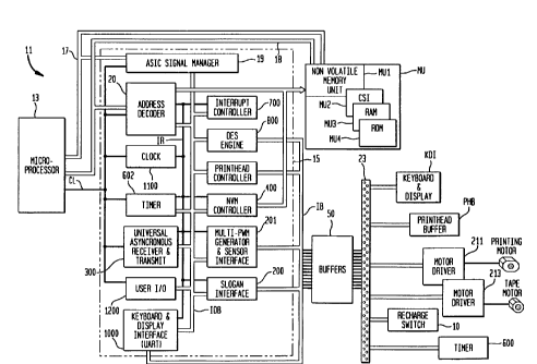
Brief Description of the Drawings
Fig. 1 is a schematic diagram of a postage metering control system in
accordance with the present invention.
Fig. 2 is a partial schematic of the ASIC address decoder unit and
ASIC NVM security unit in accordance with the present invention.
Fig. 3 is a logic schematic of the ASIC memory access and memory
security system with memory monitoring in accordance with the present
invention.
Figs. 4A, 4B and 4C are logic diagrams for ASIC memory access in
accordance with the present invention.
Fig. 4D is a logic diagram of the ASIC monitoring system in accordance
with the present invention.
Fig. 5 is a logic chart of the mainline program for the postage metering
system in a print mode and a recharge mode in accordance with the present
invention.
Detailed Description of the Preferred Embodiment
A
-5-
216 1990
Referring to Fig. 1, a microprocessor control system, generally indicated as
11,
which is preferably intended to control a thermal printing postage meter (not
shown),
is comprised of a microprocessor 13 in bus 17 and 18 communication with an
ASIC
15 and a plurality of memory units (MU). The memory units MU include secure
s non-volatile memory MU1, memory MU42, random access memory MU3 and program
memory MU4. Memory MU2 contains memory unit CS1 which is illustrative of any
memory unit of an external device (not shown) which is in communication with
the
system bus 17 and 18. The ASIC 15 is comprised of a number of integrated
circuits
modules, for example, ASIC signal manager 19, address decoder 20, clock 1100,
io timer module 602. UART module 300, user 1/0 1200, keyboard and display
interface
1000, interrupt control 700, encryption and decryption engine 800, memory
controller
400, multi-PWM generator and sensor interface 201 and a slogan interface 200.
It
should be appreciated that it is within the contemplation of the present
invention that
the IC modules which make up the ASIC 15 may vary and the modules here
identified
is are intended to illustrate the preferred embodiment of the invention.
The ASIC has an internal data bus (IDB) and a plurality of control lines one
group of which control lines are module interrupt lines IR. Another group of
control
lines CL provide a means for providing control signal from the microprocessor
13 to
the ASIC 15. Certain of the modules are in communication with a coupler 23.
The
2o coupler 23 is in communication with various meter devices, such as recharge
switch
10, timer 600, the keyboard display KDI, print head buffer PHB and motor
drivers 211
and 213. In Fig. 1, the bus lines IDB and 113, and control lines IR and CL are
depicted in simplified manner for the purpose of clarity.
Referring to Fig. 2, the microprocessor 13 communicates the read/write (R/W)
2s control signal, low data strobe (LDS) control signal, address strobe (AS)
control
signal, data bus lines D(7-0) and address lines A(7-0, 2320) to the input side
of the
ASIC 15. The RIW, LDS and data signals (D7-0) are received by a microprocessor
interface circuit 19. The processor interface circuit 19 performs a number of
interface
functions with the microprocessor. Those function relevant to the present
invention
3o will be described subsequently. The address lines and the AS signal from
the
microprocessor 13 are received by the address decoder circuit 20 of the ASIC
15.
The address decoder circuit 20 outputs a number of memory access control
signals directed to the memory security unit 400. Particularly, the address
decoder 20
directs the ROM and RAM chip select signals to the ASIC pins P3 and P4. The
3s address decoder 20 also directs chip select signals CS1 and CS2 to ASIC
pins P2
-s-
216 19 90
and P1. In the preferred embodiment of the present invention, the chip select
signals
CS1 and CS2 are provided in order to control memory access to external memory
devices (not shown). Each of the chip select signals, RAM, ROM, CS1 and CS2
are
also directed to the input side of a NVM security controller circuit 400 of
the ASIC 15.
Further directed to the input side of the NVM security controller circuit are
the select
signal (SEQ, read signal (RD), write (WR), ASIC internal memory assess select
signal
(ASIC), NVM1 select, NVM2 select and NVM3 select signals from the address
decoder 20.
Referring to Fig. 3, the address decoder circuit includes an address decoder
Io 28, an ASIC decoder 62 and a function decoder 29 which decoders will be
here
functionally described only to the extent relevant to the present invention.
The
address decoder 28 receives an AS strobe signal and address lines A(0-23) from
the
microprocessor. The function decoder 29 receives the AS strobe signal, LDS
strobe
and R/W enable signal. The NVM security circuit 400 includes an illegal
address
is detector circuit 70, more particularly described in commonly assigned US
Patent
Number 5,377,264.
A NVME register 402 and NVMD register 404 are also provided which receive
input from data lines D(7-0), the function decoder 29 and ASIC decoder 62. The
output from the NVME 402 is directed to a decryption circuit which needs a
secret key
2o from key register 406 and decrypts in the MOD 2 addition circuit 408. The
decrypted
output from the MOD 2 is compared by the comparator 410 with the encrypted
data
written to the NVMD register 404. Briefly here described, the data placed on
D(7-0) is
encrypted by the programmable microprocessor to have a specific relation to
the
decryption of that data by the Mod 2 Addition circuit. If that relationship is
detected by
2s the comparator 410, the output of the comparator 410 go active and is gated
through
gates 412, 414 and 450 to activate the NVMWR pin P5 of the ASIC under the
proper
condition subsequently described. The presence of the address strobe signal AS
which initiated the sequence of events previously described at flip-flop 462
holds the
flip-flop 462 output inactive even in the presence of a valid NVMWR signal. If
the
3o NVMWR is externally activated without the presence of an address strobe AS
signal
the flip-flop 462 is caused to change state whenever AS is next enabled
causing OR
gate 446 to go active. If the OR gate 446 goes active the state of gate 461
goes
inactive disabling gates 432, 434 and 436 which are also connected to the
output of
the flip-flop 462 through gate 454, thereby disabling unauthorized memory
access to
A
7 216 19 90
the NVMs. The output of the OR gate 446 is also directed to the microprocessor
interface unit 19 which communicates to the microprocessor the interrupt
condition.
Referring, more particularly, to Figs. 4A, 413, 4C and 4D, during an normal
write cycle, the write cycle is initiated at 950 by microprocessor 13 writing
to ASIC
registers to unlock the memory. The microprocessor 13 addresses decoder 28.
The address decoder 28 addresses the ASIC decoder 62 at 958. The address
decoder 28 then addresses the NVME register 402 and the NVMD register 404 to
receive data from the data lines 0-7 at 960. The function decoder 29 write-
enables
the NVME register 402 and NVMD register 404 to receive the data at 962. At
this
io point the software encrypted information on data line (0-7) is written to
NVME register
402 and NVMD 404 register at 464. Then, at 965 the timer 424 is then initiated
after
the write to either NVME 402 or NVMD 404 and the OR gate 422 is activated. At
966
the encrypted data from the NVME register 402 is read and combined with the
KEY,
from the KEY register 406 and decrypt by the MOD 2 408 utilizing the KEY. At
968
is the encrypted data is read from NVMD register 404 and compares with
decrypted
data from MOD 2 968 by 8 bit comparator 410. If the comparison is equal then
the
output from comparator 410 is set active at 972. If the comparison is not
equal to a
defined relationship at 970 then nothing occurs at 974. The inactive state
occurs
when spurious data is generated and written to the registers 402 and 404.
2o If a valid comparison is made at 970, the comparator 410 is activated at
972
and, at 976, the output of the comparator 410 is ANDed with the output of
timer 424
at A~!D gate 412. At 978, an AND gate 414 ANDs the output from gate 412, WR
signal from decoder 29 with the output from OR gate 416.
Subsequently, following activation of comparator 410, microprocessor 13
2s writes to one of the NVMs by addressing NVM1, NVM2 or NVM3 at 952. At 954
the
address decoder 28 produces the appropriate NVM# signal (NVM1, NVM2 or NVM3)
corresponding to the addressed NVM. Also the decoder 28 output address causes
OR gate 416 to go active at 956. Also indicated at 956, the microprocessor 13
causes the function decoder 29 to produce a WR signal. OR gate 416 in turn
3o activates gate 418. Then, address decoder 28 decodes the non-volatile
memory
address and activates gate 420 when the function decoder 29 generates WR
signal,
as described in 480 (refer to Fig. 413). If, at 482, the timer is active then
gate 426 is
turned "OFF and as a result, AND gate 430 is held "OFF" at 484. If, at 486,
the timer
is inactive, then gate 426 is turned "ON" at 488 causing AND gate 430 to turn
"ON"
_g_
216 1990
and a "INTERRUPT TYPE 1" signal to be issued, indicating a time-out condition
occurred, thereby prohibiting memory access.
Referring to Fig. 4A, at 478, an AND gate 414 ANDs the output from gate 412,
WR signal from decoder 29 with the output from OR gate 416. If, at 990, gate
412 is
s activating gate 414 active and WR is active and OR gate 416 is active, then
the
system proceeds to check to assure that no more than one memory device is
accessed at a time at 500. If not, then the system returns to location 974.
Referring to Fig. 4C, if, at 500, either ROM, RAM, CS1, CS2 select signals are
active, then OR gate 458 inactivated to turn "OFF" gate 460 at 502 and hold
AND
io gate 450 "OFF" at 504. This action prevents a nonvolatile memory write
enable signal
from being issued. If, at 500, either the ROM, RAM, CS1, CS2 select signals
are
inactive, then OR gate 458 is activated to turn "ON" gate 460 at 506. At 508,
the
output from gate 460, 452 and 414 are ANDed to turn "ON" gate 456 resulting in
the
NVMWR signal going active at 510.
is If, at 512, any two NVM1, NVM2 or NVM3 signals are active then the
corresponding AND gate 438, 440 and/or 442 is set active at 514. OR gate 444
is
then set active to turn "OFF" gate 452 at 516 which results in AND gate 450
being
held "OFF" at 518. If, at 512, any two NVM1, NVM2 or NVM3 signals are not
active
then OR gate 444 is held "OFF" resulting in gate 452 being turned "ON" at 520.
The
20 output from gate 460, 452 and 414 are ANDed resulting in gate 456 being
turned
"ON" at 522. As a result the NVMWR signal is set active at 524.
Referring to Fig. 4D, the system also monitors, at 550, the appropriate ASIC
pins to assure that the pins for NVM1, NVM2 and NVM3 detect whether the pins
are
externally drive to gain unauthorized access to the memories. In order to gain
2s access, both the NVMWR pin and one of the NVM pins P6, P7 or P8 must be
held
active. At 552, when pin 5 is externally activated without the presence of AS
signal,
the output from flip-flop 462 goes active at the next enabling of AS at 554.
As a
result, OR gate 446 is turned "ON" to issue "Interrupt 2" signal at 556. At
558, the
"Interrupt 2" signal is recorded as an unauthorized entry to memory. Now at
560, the
3o change of state of a gate 461 disables AND gates 432, 434 and 436, thereby
disabling the meter NVM memory access.
Fig. 5 illustrates a software routine that controls the operation of meter 10.
The routine commences with a determination as to whether a resetting
combination
has been inputted into the meter at step 100. If so, step 102 follows, at
which it is
ss determined whether the entered combination is valid.
-9 - ~ 16 7 .9~p
The determination of the validity of the combination may, for example, be as
described in above referenced US Patent No. 4,097,923. If the combination
was found to be valid, step 103 follows, at which the count down timer 600 is
reset. Step 104 then follows, at which the previously described routine at 450
is initiated for the purpose of incrementing the descending register is
incremented. The routine then ends. It is particularly noted that access to
the secure accounting memories is not provided until timer 600 reset is
completed.
If at step 102 the combination was found not to be valid, an error
message will be displayed through user interface 30 at step 110 and the
routine then ends.
If at step 100 a resetting combination was not input, step 112 follows,
at which it is determined whether postage printing is requested. If not, the
routine ends. If postage printing is requested, it is next determined, at step
114, whether there are sufficient funds in the vault, i.e., whether the
descending register has a reading sufficiently high to permit printing of the
requested postage amount at step 114. If there are not sufficient funds, an
error message is displayed at step 110 and the routine ends: If there are
sufficient funds at step 114, then at step 116, a check is performed to see if
timer 600 has timed out. If the timer 600 has timed out, then an error is
displayed to the user at step 110 and the routine ends. If the timer 600 has
not timed out, then step 120 follows, at which the meter prints postage
through print mechanism 24 and then updates the secure registers in the
non-volatile memory unit MU by adding the amount of postage dispensed to
the ascending register and subtracting that amount from the descending
register. The routine then ends.
The metering system advantageously also includes a routine for
testing whether the time deadline will soon be reached and displaying a
warning of this fact. Additional steps to accomplish these functions may
readily be inserted, for example between steps 116 and 120 of Fig. 2.
It is observed that the security process for accessing the non-volatile
memories is quite elaborate in order to protect the non-volatile memory from
receiving unintended data with the potential of corrupting the accounting
data. The present invention provides an improved system of providing a time
lock-out without endangering the security to the non-volatile memories.