Note: Descriptions are shown in the official language in which they were submitted.
21~~9~4
1 RCA 87,698
DIGITAL VIDEO SIGNAL PROCESSING SYSTEM INCLUDING A
CO-CHANNEL REJECTION FILTER
This invention is related to the field of digital signal
processing, and more particularly to a television signal receiver
system including a filter for rejecting co-channel interference.
Recent developments in the field of video signal processing
have produced digital high definition television (HDTV) signal
processing and transmission systems. An HDTV terrestrial
broadcast system recently proposed as the Grand Alliance system
in the United States employs a digital transmission format for
transmitting a packetized datastream. The Grand Alliance HDTV
system is a proposed transmission standard that is under
consideration in the United States by the Federal Communications
Commission through its Advisory Committee on Advance
2 0 Television Services (ACATS). A description of the Grand Alliance
HDTV system as submitted to the ACATS Technical Subgroup on
February 22, 1994 (draft document) is found in the 1994
Proceedings of the National Association of Broadcasters, 48th
Annual Broadcast Engineering Conference Proceedings, March 20-
2 5 24, 1994.
The proposed Grand Alliance HDTV system is a simulcast
system. In such a system, two versions of the same program
material may be broadcast simultaneously via separate standard
3 0 6 MHz channels. One of the two program versions contains
standard definition NTSC information broadcast on one channel,
while the other contains high definition information broadcast on
the other 6 MHz channel. In practice, a simulcast system may
utilize two adjacent 6 MHz NTSC channels, eg., VHF channels 3 and
3 5 4, to convey the standard and high definition information,
respectively. The high definition version of a simulcast system can
2 RCA 87,698
be implemented in a standard 6 MHz channel by using data
compression techniques. The standard NTSC information and the
HDTV information are received independently by respective
standard NTSC and HDTV receivers. When standard NTSC
receivers are eventually replaced by HDTV or dual-standard
receivers, the channels used by standard NTSC signals will become
available for other purposes. Thus the simulcast concept prevents
the vast number of pre-existing standard NTSC receivers from
becoming obsolete as soon as HDTV broadcasting is introduced,
and permits expanded broadcasting services in the future when
the channels occupied by standard NTSC signals become available.
The rejection of co-channel interference is a factor in a
simulcast system since co-channel interference may severely
degrade or disrupt the operation of a high definition television
receiver. Co-channel interference may result when two different
television signals are transmitted on the same broadcast channel
and are received simultaneously. The interfering signal
components typically are the picture carrier (located 1.25 MHz
2 0 from the lower band edge), the chrominance subcarrier (located
3.58 MHz higher than the picture carrier) and the sound carrier
(located 4.5 MHz higher than the picture carrier). The likelihood of
co-channel interference occurring is a function of various factors,
such as the broadcast distance between the two channels and the
2 5 transmission power of the channels, for example.
In accordance with the principles of the present
3 0 invention, a digital signal processing system for receiving and
processing a video signal, eg., in a Quadrature Amplitude
Modulation (QAM) format or a Vestigial Sideband (VSB) format,
includes a network for rejecting an interferes signal such as a
continuous wave NTSC co-channel interferes signal using an FIR
3 5 filter in a carrier recovery loop. In an illustrated embodiment, co-
channel rejection is accomplished by an FIR digital filter following
~1~1~~4
3 RCA 87,698
an equalizer and situated in a carrier recovery loop which brings a
near-baseband signal to baseband. The filter enhances the
performance of both the equalizer and the carrier recovery
network.
Brief Description of the Drawings
In the drawing:
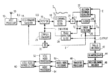
Figure 1 is a block diagram of a portion of a high definition
television receiver system including a co-channel notch filter
network in accordance with the principles of the present
invention.
Figure 2 illustrates amplitude-frequency responses for
baseband QAM and NTSC co-channel signals.
Figure 3 illustrates an amplitude-frequency response of the
notch filter network in the system of Figure 1.
Figures 4 and 5 respectively show the Real and Imaginary
time domain responses of the filter network of Figure 1.
2 5 Figure 1 is a block diagram of a portion of a high definition
digital television signal receiver. In this example a QAM signal,
which is a type of pulse amplitude modulated (PAM) signal, is
received and processed. As is known, in a QAM symbol
transmission system a transmitted data symbol is represented by
3 0 quadrature components which modulate respective quadrature
phased carriers at a given frequency. Each symbol is mapped
(assigned) to a prescribed coordinate in a four-quadrant grid-like
constellation. In a 32-QAM system for example, each quadrant of
the constellation contains eight symbols at prescribed coordinates
3 5 with respect to I and Q quadrature axes.
~1~~99~
4 RCA 87,698
A broadcast high definition QAM television signal received
by an antenna 10 is applied to an input processor 12. Processor 12
includes a tuner and intermediate frequency (IF) stage for down-
converting the received signal to a lower frequency band above
S baseband, automatic gain control networks, and an analog-to-
digital converter, for example. Input processor 12 may also
include networks for Nyquist-rate sampling a bandpass filtered
input signal, phase splitting the filtered input signal into
quadrature I, Q components, performing a preliminary
demodulation, and performing twice symbol rate sampling prior
to feed-forward equalizer 14. The preliminary demodulation
brings the signal close to baseband so that the receiver does not
have to operate on the high frequency input signal. Also included
in input processor 12 (but not shown to simplify the drawing) is a
timing/clock recovery network for developing a symbol rate clock
from the received QAM signal. Timing/clock recovery networks
for recovering a symbol rate clock from a received signal are well
known and are described, for example, in the reference text
Digital Communication, Lee and Messerschmitt (Kluwer Academic
2 0 Press, Boston, MA, USA, 1988).
A passband I, Q digital QAM signal from unit 12 is processed
by passband feed forward adaptive equalizer 14, eg., a
fractionally spaced equalizer, which conditions the signal before
2 5 further processing. Specifically, equalizer 14 includes an adaptive
digital FIR filter which compensates for transmission channel
perturbations such as frequency/phase irregularities. Equalizer 14
responds to dynamically updated filter coefficients generated in
response to a control signal as will be discussed, after an
3 0 initialization interval during which equalizer 14 is initialized using
blind equalization or using training signal techniques.
An equalized passband signal from equalizer 14 is complex
in nature with Real and Imaginary components, and may be at or
3 5 near baseband. This signal may be symbol rate sampled before
being processed by a rotator 16, which is sometimes referred to as
~is~~~~
RCA 87,698
a de-rotator in view of its function in a carrier recovery network
for bringing near-baseband signal frequencies to baseband signal
frequencies. Rotator 16, eg., a complex multiplier as known,
compensates for a dynamic phase error manifested by a slight
5 rotation of the received QAM constellation. This error may be
produced by a variety of factors including local oscillator
frequency variations, for example. The constellation phase
error/rotation may be significantly reduced or eliminated by the
carrier recovery network, the operation of which resembles a
1 0 baseband demodulator. In this example the carrier recovery
network includes a control loop comprising rotator 16, adder 20,
slicer 24, error detector 26 and a phase detector and voltage
controlled oscillator (VCO) network 28, which develop an error
signal E for use as will be discussed. Units 16, 24, 26 and 28
comprise the essential elements of a digital phase locked loop
(PLL) for eliminating the dynamically varying carrier offsets. The
carrier recovery loop also advantageously includes a co-channel
rejection filter 18 as will be discussed.
2 0 The received QAM signal may be contaminated with an NTSC
co-channel interferer information as shown in Figure 2, which
illustrates the amplitude-frequency spectrum of the QAM signal
relative to narrowband co-channel NTSC interferer components at
the picture carrier and chrominance carrier frequencies. To reject
2 5 the co-channel interferer components, co-channel notch filter 18
in accordance with the principles of the present invention is
included in the control loop described above, after rotator 16.
Filter 18 processes baseband (and near-baseband) signals from
rotator 16 with an amplitude-frequency response as shown in
3 0 Figure 3, with high attenuation (notches) at the picture carrier and
chrominance subcarrier baseband frequencies. The Real and
Imaginary time domain responses of filter 18 are illustrated by
Figures 4 an 5, respectively, where T designates a symbol interval.
~1619~4
6 RCA 87,698
Filter 18 is a linear phase causal bandpass digital FIR filter
with substantially zero throughput delay. The Z-transform domain
output response N(z) of filter 18 is defined by the expression
N(z) = 1 + Z-1C(z)
The term C(z) in the above expression represents the trailing
response of filter 18. The coefficients of filter 18 are weighted to
provide the described attenuation notches at the baseband picture
and chrominance carrier frequencies.
Referring to Figures 2 and 3, it is seen that the filter 18
response does not include a rejection notch at the sound carrier
frequency at the high end of the baseband. This is because, in this
example, the system parameters are chosen so that the sound
carrier resides on the Nyquist slope in the excess bandwidth
region (i.e ., the filter slope at the high frequency end). Nulls for
the audio carrier may also be created by equalizer 14.
It is noted that filter 18 is advantageously located after
rotator 16 in the carrier recovery network. In this regard the
2 0 inventors have observed that if filter 18 is placed before feed-
forward equalizer 14 and a carrier frequence offset is present, the
filter attenuation notches will not be properly aligned with the
picture and chrominance carrier frequencies that are to be
attenuated. If the notch filter is positioned before the rotator,
2 5 wider attenuation notches should be used to account for the
possibility of a carrier frequency offset. The disclosed location of
filter 18 after rotator 16 advantageously permits the use of
narrow notches with a sharp attenuation characteristic at the co-
channel frequencies to be attenuated, resulting in efficient
3 0 filtering. In addition, the zero delay characteristic of filter 18 does
not compromise the pull-in and tracking characteristics of the
carrier recovery loop.
A notch filter corresponding to filter 18 may be used to
3 S reject any continuous wave interferer signal, not only co-channel
NTSC picture and chrominance carrier frequencies as disclosed in
~1fi~9~
7 RCA 87,698
the illustrated embodiment. Although filter 18 preferably exhibits
a zero delay, a nominal amount of delay may be tolerated as a
function of the operating parameters of a given system.
The filtered baseband output signal from filter 18 is applied
to an additive input of a subtractive combiner 20, a subtractive (-)
input of which receives an output signal from a decision feedback
equalizer 22. The output signal from combiner 20 is processed by
a slicer 24. Slicer 24 contains a mapping mechanism and is
programmed to select the constellation symbol that is closest in
distance to the received signal sample. The complex (I, Q) QAM
constellation is divided into decision regions where each decision
region is the set of points that is closest to some symbol. If, after
examining a decision region for a symbol, a received symbol is
found to be located at or offset in distance from an expected
coordinate, slicer 24 produces an output symbol at the expected
coordinate. The slicer output symbol differs from the dicer input
symbol by the amount of any distance offset. The amount of any
such offset is sensed by error detector 26, which produces an
2 0 output error signal "E" as a function of the amount of the offset.
This error signal is used to adjust the tap coefficients of equalizer
14 (via multiplier 30) and equalizer 22 so as to bring the error
value to zero, such as through the use of a Least Mean Squared
algorithm as is known.
Signals S; and So at the input and output of dicer 24,
respectively, are provided to a phase control unit 28 including a
phase detector and voltage controlled oscillator (VCO) for
generating output sine and cosine quadrature correction
3 0 coefficients. Associated with each sine and cosine correction
coefficient is an error correction phase angle which is a function of
the value of error signal E. The output correction coefficients from
phase control unit 28, and the QAM I, Q constellation components
from equalizer 14, are provided to respective inputs of rotator 16
3 5 to perform the (de)rotating function for producing baseband
output signals from rotator 16. It can be shown that any set of
~~.6~,99
8 RCA 87,698
quadrature signals can be rotated to a desired angular position by
performing a complex multiplication on the quadrature signals.
Decision directed feedback equalizer 22 processes the output
S signal of slicer 24, and has its coefficient values controlled as a
function of the value of error signal E. Error signal E is also
provided to one input of a complex multiplier 30, another input of
which receives sine and cosine output signals from phase control
unit 28. These signals are converted to complex conjugate form by
a unit 29 before being applied to multiplier 30. An output
passband error correction signal from multiplier 30 is applied to a
control input of equalizer 14 for controlling the coefficient values
of equalizer 14 to facilitate the equalizing operation.
Filter 18 advantageously enhances the performance of
equalizer 14 by assuring that proper coefficient control signals are
applied to equalizer 14 from unit 30. Since filter 18 is located in
the carrier recovery loop where a baseband signal is recovered,
the co-channel rejection notches of filter 18 are accurately aligned
2 0 with the associated baseband signal frequencies to be rejected.
Consequently, error signal E and the coefficient control signals
accurately reflect the baseband signal characteristics. This result
would not be obtained if filter 18 preceded equalizer 14.
2 5 The placement of filter 18 also advantageously enhances the
carrier recovery operation by providing an accurate signal at the
input of dicer 24, i.e ., a signal with properly rejected co-channel
frequencies. Slicer 24 co-acts with error detector 26 to generate
phase error signal E, which is used to control the coefficients of
3 0 equalizers 14 and 22 as discussed.
The combination of elements 16, 20, 24, 26 and 28 form a
carrier recovery loop for providing a baseband demodulated
signal at the output of rotator 16. With the exception of filter 18
3 5 in accordance with the principles of the present invention, these
elements form a carrier recovery loop as described in the Lee and
~16199~
9 RCA 87,698
Messerschmitt text mentioned earlier. This text also discusses the
operation of feedback equalizer 22, and the coaction of multiplier
30 with feed-forward equalizer 14. Forward equalizer 14 is a
filter that also removes some of the Inter Symbol Interference
(ISI). Feedback equalizer 22 then removes the rest of the ISI,
including any ISI generated by filter 18.
Decision feedback equalizer 22 may be preloaded with
coefficients with function C(z) such that the overall response of
equalizer 22 is related to the function
1
1 + Z-1C(z)
This response effectively creates a noiseless pole which effectively
cancels the notches created by the filter 18 response N(z) noted
previously. The poles are noiseless since the input to unit 22 is the
result of noiseless decisions from dicer 24.
The baseband Output signal from dicer 24 is decoded by
means of a Viterbi decoder 42, de-interleaved by unit 44,
2 0 subjected to Reed-Solomon error decoding by unit 46, and applied
to a transport processor 48. Processor 48 transports a decoded
output signal from unit 46 to appropriate decoders within unit 50
depending on the content of the signal from unit 46, eg., audio or
video information. Transport processor 48 receives corrected data
2 5 packets from unit 46 and examines the header of each packet to
determine its routing. Audio and video output signals from unit
50 are respectively applied to an audio processor 54 and to an
NTSC television video processor 52, which place the signals in a
format suitable for reproduction by a unit 60.
Although the system of Figure 1 was described in the
context of a QAM input signal, other types of pulse amplitude
modulation (PAM) input signals including QPSK signals may also
be used, as well as vestigial sideband (VSB) input signals.