Note: Descriptions are shown in the official language in which they were submitted.
WO 94/28452 216 216 B PCT/US94/05911
-1-
OPTO-ELECTRO-MECHANICAL DEVICE OR FILTER, PROCESS
FOR MAKING, AND SENSORS MADE THEREFROM
This invention relates to devices and their applications which employ a
resonant
semiconductor member whose vibratory motion is coupled to the radiant energy
cast
onto a photovoltaic energy conversion device. It also relates to such devices
whose
vibratory behavior is otherwise affected and which affect can be read
optically. These
devices may even be self resonant. Throughout this patent, the terms light and
optical
or radiant energy are used as equivalent terms and intended to have their
broadest
meaning, covering all useful forms of radiant energy.
To date no known resonant devices have been driven with direct optical-electro-
mechanical coupling. This invention is, and is readable optically. There have
been
some opto-thermal-mechanical devices driven by temperature changes resulting
from
absorbed radiation which are described in the literature, however these
devices use
neither the structures nor principles taught here. For reference to opto-
thermal drives,
see for example "Optical Micromachined Pressure Sensor for Aerospace
Applications",
by Diogenes Angelidia and Philip Parsons, Optical Engineering, Vol. 31(1992)
pp.
1638-1642. See also "Optical Excitation of Mechanical Microresonators", Kozel,
et al,
Soviet Tech. Phys. Lett. 17(11), Nov. 1991 0360-120X/91/11 0 804-02 (D Am.
Inst. of
Physics, 1992), and "Photothermal Self Excitation of Mechanical
Microresonators", also
Kozel, et al, Opt. Spectroscopy (USSR) 69 (3), Sept. 1990, 0030-400x/90/090401-
02
(D 1991, The Optical Society of America).
Other interesting variations for resonant beam drives are described in
"Optical
Fiber Sensors Using Micromechanical Silica Resonant Elements" by Jones, Naden
and
Neat, IEE vol. 135(part D)(1988) pp 353-8 and in "Photoacoustic Oscillator
Sensors"
by Langdon and Dowe, SPIE, Vol. 798, Fiber Optic Sensors II (1987), pp 86-93.
It
should be noted that in the Jones, Naden and Neat article, these researchers
were
convinced that it would be possible to construct a self resonant device that
was excited
optothermally (using the thermoelastic effect), although they believed silicon
for this
purpose was unsuitable (page 358). U.S. Patent 5,188,983 assigned to Wisconsin
Alumni Research Foundation, inventors being Guckel and Sniegowski, and an
International Application No. PCTUS93/08404 assigned to Honeywell Inc.,
inventors
CA 02162168 2003-07-28
50796-1
2
being Zook and Burns, describe relevant teaching within the
prior art relative to resonant microbeams incorporating
electrostatic drive and piezoresistive sense. In these
cases, electrostatic excitation is achieved using force
generated by applying small alternating voltages to
stimulate the microbeam. Sensing of the microbeam flexure
is achieved using strain sensitive resistive elements.
Oscillatory behaviour requires electronic amplification and
phase correction circuitry. The approach disclosed herein
uses optical methods to drive the microbeam, sense the
microbeam vibrations and, if certain conditions are met,
produce self-oscillation with no intervening electro-optical
components, thus eliminating the need for piezoresistors,
drive electrodes, electrical contacts and any metallurgy for
electrical interconnection. The resulting simplification in
microbeam construction reduces processing steps, eliminates
sources of aging or degradation, allows for better matching
between microbeams and allows for significantly thinner
microbeams for increased sensitivity while reducing chip
size and cost.
For background or construction techniques useful
in building structures similar to what is described here,
see POLYSILICON RESONANT MICROBEAM TECHNOLOGY FOR HIGH
PERFORMANCE SENSOR APPLICATIONS by Guckel, et al, 0-7803-
0456-X/92, (~ 1990, IEEE).
EP-A-0451992 describes a polysilicon resonating
beam transducer having a resonant beam positioned above a
cavity formed in a semi-conductor substrate. A portion of
the beam and substrate are doped to render them electrically
conductive to form electrodes so that the beam can be driven
capacitively by an applied voltage. In an alternative
embodiment, an electrode is formed above the resonant beam
and a voltage is applied between the electrode and the beam
CA 02162168 2003-07-28
50796-1
2a
by means of a photovoltaic device connected thereto which is
driven by a pulsed light source.
EP-A-0400939 describes a semi-conductor sensor
with a vibrating element positioned above a cavity formed in
an n-type semiconductor substrate. A p-type region is
formed in the base of the cavity which serves as an
electrode to capacitively drive the beam into resonance on
application of a drive voltage between the beam and p-type
electrode.
In general the device herein has two potential
basic forms: a device having a self-resonating member,
drivable by either a continuous or pulsed/modulated optical
signal; and a device with a flexible member which is driven
to resonance by an optical signal of timed pulses. In
general, either one affects an optical input at a rhythm
related directly to the vibrations the member makes, since
the moving member's reflectivity is changing cyclically with
each oscillation. (A third form is also described which
uses a reverse biased p-n junction photodiode that only
resonates in the presence of light. This third form has
significant advantages and disadvantages as well.)
These vibrations of the flexible member and their
rates are affected by the other environmental influences on
the resonating member, for example; stress and strain,
temperature, pressure, acceleration, acoustic influences,
and so forth. Variations in the structure of the member may
be made to get better signal-to-noise ratio for the
influence being measured, so, for example, a short
cantilevered beam would be better for temperature sensing
and a relatively long beam attached at the two longitudinal
ends would be better for sensing strain. Multi-beam devices
are also useful. A number of variations are taught herein.
CA 02162168 2003-07-28
50796-1
3
Accordingly, many real sensing needs may be easily
met using this invention, including, for example, pressure,
weight, temperature and so forth. Further, these devices
may be added to larger structures, such as a larger
diaphragm, for example, to calibrate it or give more exact
readings than would otherwise be available by direct
measurement of a larger diaphragm using capacitive,
resistive or other sense originated signals.
Many variations in the structure itself are
possible while staying within the scope of the teachings of
this patent, and are covered by the claims herein.
SUMMARY OF THE INVENTION
According to the present invention, there is
provided a device comprising a semiconductor base having a
cavity formed therein, a flexible member formed of a
semiconductor material and connected to said semiconductor
base such that said flexible member can flex towards said
cavity and photovoltaic drive means for receiving radiant
energy transmitted into said cavity to cause said flexible
member to flex and wherein said device is optically coupled
to an optical guide for directing radiant energy into said
cavity.
Also according to the present invention, there is
provided a device comprising a semiconductor base having a
cavity formed therein, a flexible member formed of a
semiconductor material and connected to said semiconductor
base such that said flexible member can flex towards said
cavity and photovoltaic drive means for receiving radiant
energy transmitted into said cavity to cause said flexible
member to flex, wherein said device is optically coupled to
CA 02162168 2003-07-28
50796-1
3a
a source of radiant energy for introducing radiant energy
into said cavity.
According to the present invention, there is
further provided a device comprising a flexible member
formed of a semiconductor material, photovoltaic drive means
for causing said flexible member to flex when said
photovoltaic drive means is exposed to incident radiant
energy, said photovoltaic drive means being disposed
opposite and spaced from said flexible member and defining a
gap therebetween, and wherein said device is optically
coupled to an optical guide for directing radiant energy
onto said photovoltaic drive means.
According to the present invention, there is
further provided a device comprising a flexible member
formed of semiconductor material and a photovoltaic drive
means for causing said flexible member to flex when said
photovoltaic drive means is exposed to incident radiant
energy, said photovoltaic drive means being disposed
opposite and spaced from said flexible member and defining a
gap therebetween, and wherein said device is optically
coupled to a source of radiant energy arranged to direct
light onto said photovoltaic drive means.
According to the present invention, there is
further provided a device comprising a flexible member
formed of a semiconductor material, a photovoltaic drive
means for causing said flexible member to flex when said
photovoltaic drive means is exposed to radiant energy, said
photovoltaic drive means being spaced from said flexible
member and defining a gap therebetween, and wherein said
flexible member is adapted to permit radiant energy to pass
therethrough to said photovoltaic drive means.
CA 02162168 2003-07-28
50796-1
3b
An embodiment of the present invention in a most
simple form requires merely that a resonant microstructure
member of one electrical type (p or n) be formed over a
wafer, this member extending substantially or fully over a
cavity or other space in the wafer. At a location in a wall
or floor of the cavity is a region of opposite type (p or n)
material. The interface between the two types is known as a
p-n junction and is the best known form of a photovoltaic
structure. The location of this photovoltaic structure is
important. The flexible member and the opposite type region
should be substantially in the path of the driving radiant
energy (hereinafter called "light" for short). In another
embodiment of the invention, the driving light may fall on a
region of the same type as the member if that region is
coextensive electrically with said member and the member is
located across a cavity or spaced apart from an oppositely
typed region. The photovoltaic device in the base can also
be formed by methods other than a p-n junction. These
include a p-i-n diode, a metal-semiconductor junction or
surface states which cause the surface potential to be
different from the bulk. Such surface states can result in
a partially depleted, fully depleted, or inverted surface
layers. All these structures can exhibit photovoltaic
effects sufficient to drive the flexible member. Herein
references to "opposite type" material or regions refers to
any photovoltaic structure. The location of the
photovoltaic structure is important.
An analogy of the motion of the member might be
made to that of pushing a baby on a swing; one pushes when
the swing has begun its downward motion. In other words,
the driving force to maintain the oscillation must be in the
same direction or in
WO 94/28452 216 216 8 PCT/US94/05911
-4-
phase with the velocity. To complete this analogy, the driving voltage
attracting the
member is maximum when the member is moving toward that oppositely typed
region.
The devices of this invention act as opto-electro-mechanically coupled
photodiodes--causing the movable or flexible member to be attracted
electrostatically to
the opposite type region by the incident driving light. Thus, it couples the
optical
energy to mechanical resonance or motion through the electrostatic force
generated by
the photodiode. We disclose herein what we believe to be the reasons it
operates the
way it does, however, other physical theories may eventually show its cause of
operation to be different. Nevertheless, no one has taught a device structure
that directly
couples optical energy electrostatically to mechanical energy in any similar
manner
before. Furthermore, the close proximity of the flexible member to the
substrate or to an
integrated cover or top cap forms a Fabry-Perot interferometer capable of
producing
large intensity modulations of the reflected light with small displacements of
the
member. To re-emphasize, to the best of the inventors' knowledge, no one has
ever
1 S taught a device structure which directly couples optical energy
electrostatically into
mechanical energy in any manner similar to this instant invention before.
A preferred form would have the vibratory member located within an evacuated
capsule. T'he top cap would seal the member off on one side, and the wafer on
which it
was mounted or formed would seal the other. A currently preferred form would
have
the light be incident normal to the member, with the opposite type region
positioned to
be directly in that light path beneath the member. Evacuated and encapsulated
forms are
preferred. However, non-evacuated forms and other less than optimal
constructions are
useful and acceptable for devices, for example, where a pulsed or modulated
light signal
is used to drive the flexible member and where self resonance is not necessary
or
desirable for the use to which this invention is to be put.
The optical pathway may also be at an angle to a covering and be reflected
through the resonant member to an appropriately positioned opposite type
region.
Variant forms having leaky cavities of various shapes, or flaps, or hinged
coverings of holes in the members may be used for pumping fluids. Other
variant forms
having multiple flexible members, members of various shapes and multiplicities
of
opposite type regions can be built. This invention could, for example, be used
to drive a
microencapsulated tuning fork.
,WO 94128452 PCT/US94/05911
-5-
In its presently most preferred form the thickness of the flexible member
should
be an odd multiple of one quarter the wave length of the driving light, and
the cavity or
space between it and the region of the opposite type should be somewhat less
than a
multiple of half the wavelength of the incident light. The cavity above the
flexible
member and the vacuum enclosing shell should be somewhat greater than one-half
a
wavelength. The flexible member vibrates between its preferred extreme
positions at
7,12 and 7J4. (Note that any of the distances can always vary by adding or
subtracting
a,/2 or multiples thereof since the reflections will have the same phase
relationships.)
If a cap is used on the side of the member opposite the opposite typed region,
it
should be spaced so that the sum of the cavity spaces on both sides of the
vibrating
member are an even multiple of one-half wave length.
In its presently most preferred form, as a strain transducer, the flexible
member
is a beam, clamped at both ends, with the photovoltaic device under the beam.
A
reference transducer responsive to temperature would use a beam clamped only
at one
end. The thickness of the microbeam and of the spaces above and below it
should be
chosen so that the light transmitted to the photovoltaic device increases when
the beam
is deflected away from the photovoltaic device (or area of opposite type), and
decreases
when the beam is deflected by its own restoring force toward the opposite type
area.
Since the electrostatic force between the drive electrode and the flexible
member
increases with light intensity this arrangement results in positive feedback
condition
useful for self resonant behavior. This "positive feedback" is perhaps better
explained
with reference to the figures later.
This implies a photovoltaic device which can develop drive voltage under
suffcient illumination to make this a dynamic device, i.e., the rest position
of the beam
is unstable and it begins to resonate. Thus, this invention describes a member
of the
class of so called "active devices."
Even in cases where the member/cavity/cap/opposite-type-region arrangement is
not in the most preferred spacing configuration, a pulsed or modulated light
source can
be used to drive the member into a resonant oscillation related to the timing
of the
driving light pulses. A modulation in the signal derived from light reflected
from the
surface of the member will be caused by environmental changes (strain,
temperature,
etc.) affecting the flexible member's resonant frequency. Long members or
beams
WO 94/28452 PCT/LJS94105911
-6-
exhibit other characteristics of vibratory movement that can also be used. For
reading
frequency, there are at least four methods: self resonance, a phase-locked-
loop which
makes the modulating driving light synchronous with the resonant frequency,
"ring
down" of the peaks of reflected light signal returned by reflection from the
surface of
the flexing member, and frequency scanning wherein the modulation frequency of
the
driving light is scanned.
The presently preferred way of receiving the reflected light is through the
same
optical pathway that delivers it. The reflected light path (preferably an
optical fiber or
an integrated waveguide) has a beam splitter(preferably a 3db fiber optic
coupler) that
will divert the reflected light to a photodetector and a signal representing
the motion of
the member in vibration will result, corresponding to a minimum signal at the
point
where the member is farthest to the opposite type region and a full signal as
it travels to
a point nearest the region. This beam splitter can be in the fiber optic
cable, which may
be set in guides on the same chip as the resonant device, although other wave
guide
structures may be used. A figure describing a similar optical system is in the
Kozel, et
al article of September 1990, cited above. Integrated silicon-nitride
waveguides can also
be used as a preferred technique to transmit the incident radiation to the
shell and reflect
it downwards through the shell and beam and into the photovoltaic device or
region.
The same waveguide would carry the return light.
Flexible member resonance has been studied with respect to beam-shaped
members. See for example Zook, et al, "Characteristics of Polysilicon Resonant
Microbeams", D El Sevier Sequoia, 1992. Sensors and Actuators A, 35 (1992) 51-
59,
which describes the characteristic resonant frequencies, including multiple
resonance
frequencies. While it is convenient to use the term 'microbeam' to describe
the resonant
member, the invention is not limited to beam-shaped members only. In this
description,
the term 'beam' will be used only to refer to a beam of light, in order to
avoid
confusion.
Devices using the claimed invention can be used for example to measure the
speed of a rotating shaft where they are placed in association therewith such
that light
strikes them only some limited number of times (for example one) per rotation,
since the
resonant frequencies of the member are much higher than the rotation rate of
the shaft.
WO 94/28452 21 b 216 8 PCT/US94/05911
Such devices can also be used to measure temperature, pressure, strain, force,
acceleration, or as timers, where they are isolated from such disturbances.
They can be
used as microphones, hydrophones, light modulators, and acoustic emission
devices.
Numerous member/cavity/opposite-type region configurations are possible with
currently available technology and the drawings herein can represent only a
few.
Devices built in accord with this teaching have the obvious and significant
advantages of low power, high noise immunity, high signal to noise ratio,
digital-optical
output, no metalization required on the chip, and the ability of self
resonance in certain
preferred forms. They can also be used as magnetic field sensors, amplifiers,
mixers,
filters, and corrosion sensors. Furthermore, when coupled with a dissimilar
material in a
bimorph configuration, they can be used to measure magnetic fields, electric
fields,
humidity, temperature, chemical adsorption or as proximity sensors.
It should be appreciated that although a p-n junction photodiode provides the
easiest visualization of the device operation and is explicated throughout
this teaching,
any physical mechanism which generates a photovoltage such as a p-i-n
junction, a
metal-semiconductor junction or partially depleted, fully depleted or inverted
surface
states would suffice. The preferred construction material is currently
silicon, single
crystal or polycrystalline, although particularly useful applications may be
had from
structures constructed of SiC, Diamond, GaAs, AIGaN, GaN, or GaAIAs, or other
III-V,
2a or II-VI compounds. These materials are preferred because they share
properties that
allow operation at elevated temperatures. For high temperature applications it
would be
advantageous to use a wide-bandgap semiconductor such as GaN, which has
piezoelectric properties and a bulk photovoltaic effect which can be used at
high
temperatures. It appears currently to be of great advantage not to require
metalization
anywhere on the chip, however, some metalization is possible and for some
situations
may be useful and desirable.
All that is required is construction materials having a suff=iciently high-Q
and
large enough index of refraction to give an adequate change in reflection of
the structure
at the sense wavelength when the member vibrates.
BRIEF DESCRIPTION OF THE DRAWINGS
Figs. 1 a, I b, and 1 c are sectional views through the upper portion of a
wafer
containing a device constructed in accord with one preferred embodiment of the
WO 94128452 - 216 216 8 PCT/US94/05911
_g_
invention; each illustrating a different moment in the oscillatory movement of
the
flexible member thereof.
Figs. 2a, 2b, 2c and 2d are line graphs illustrating the rise and fall with
respect to
time of the member displacement (2a), velocity(and the negative of the
frictional force)
(2b), the transmitted light intensity reaching the oppositely typed region and
restoring
force (2c), and the amount of electrostatic drive force on the beam (2d),
respectively.
Fig. 3a is a cross-sectional side view of one preferred embodiment.
Fig. 3b is a heuristic diagram representation of Fig. 3a.
Fig. 3c is a heuristic energy conversion cycle diagram.
Figs 4a, 4b and 4c are cross-sectional side views illustrating both one
preferred
embodiment of the invention, and the concept of optothermal drive. Fig 4d
illustrates a
variation having two oppositely typed regions.
Figs. Sa, Sb and Sc are cross-sectional side views of alternate preferred
embodiments.
1 S Figs. 6a, 6b, 6c, 6d, and 6e and 6f and 6g are heuristic diagrams of
applications
of this invention associated with an accelerometer, and two pressure sensors,
respectively, each shown in cut-away side view.
Fig. 7 is a cut-away side view of an alternate preferred embodiment.
Fig. 8 is a cut-away side view of another alternate preferred embodiment.
Figs. 9a-g are side views of a preferred wafer processing series of steps to
create
one embodiment of the invention.
Fig. 10 is a block diagram of a preferred embodiment.
Figs. l la and l lb are top and cut-away side views of another preferred
embodiment.
Fig. 12 is a line graph of gap spacing versus reflectivity for three variant
forms
of preferred embodiments.
Fig. 13 is a cut-away side view of another preferred embodiment.
Fig. 14 is a side view of a device in accord with one preferred embodiment not
having a top cap or covering capsule.
Fig. 15 is a plan view of selected microbeam geometries.
WO 94/28452 216 216 8 PCT/US94/05911
-9-
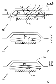
Refer first to Figs. 1 a, b and c in which a basic version of the device 10
capable
of exhibiting the self resonant qualities is described. The structvire
functions as an
optical interference filter that modulates the driving light striking the
photovoltaic
device in the base. The device is formed on the surface (called an upper
surface for
S convenience herein) 20 having, in the preferred embodiment, the ordinary
electrical
property type (n-type) forming all of the device except for an p-type region
30 at the
base of a cavity 31 that separates the flexible member 40 from the area in
which the
opposite typed region 30 is located. (For some user's applications a device
constructed
from the reverse order of material types may be preferable but for heuristic
purposes we
will stick to this arrangement. For this and other reasons it should also be
noted that the
theory of operation described herein should not be taken as limiting in any
way. Only
the claims limit the scope of protection afforded this invention.)
The p-n junction functions as a photovoltaic device, generating a voltage
between the n- and p- regions in response to incident driving light. (In the
nonself
resonant mode of operation(although this may be used for self resonant devices
too), the
driving light is modulated, and a separate unmodulated beam with a different
wavelength or direction is preferably used for reading, although the
reflections of the
driving light may also be used as well as piezoresistive strips on the beam or
capacitive
or magnetic sense of the beam position.) Another part of the cavity 41
separates the
2U member from an outer, or top, cap layer 50. Optical input energy (or
driving "light") is
referred to here by the arrow (a) which strikes the device at an orientation
which may be
but need not be normal to the surface of the wafer 20, the flexible member (or
beam) 40,
and the cap 50.
In Fig. la the device 10 is at rest with the beam 40 in a low energy or static
2S equilibrium position. The arrival of light striking the region of opposite
type 30 causes
charge to build up there, creating an electrostatic attraction to the beam or
flexible
member 40, causing it to flex toward region 30. The extension of member 40
toward
region 30, in accord with this embodiment, is illustrated in Fig. lb. (It
should be noted
that it is preferred that the maximum extension of the beam downward not reach
the
30 lower surface of the cavity.) In order to illustrate the presently most
preferred form,
refer to Figs 1. Note that the device in a Fig. 1 a state has a set of
measurements where
hl is some multiple of 37v,/8, of h2 is Sa,/8, and the measure of h3 is 7J4n,
where n is the
WO 94/28452 PCT/US94/05911
-10-
refractive index of the semiconductor of which it is formed. (It is well
understood that
adding thicknesses to hl, h2, or h3 in multiples of 1/2 the wavelength of the
light does
not affect the interference and therefore any such multiple may be used in the
completed
product without affecting the functioning of the device.)
The device in Fig. 1 c forms a "quarter-wave stack", the first cavity (31 )
(height
hl), being 7~/4 (or an odd multiple thereof), the beam itself (h3) being also
an odd
multiple of ~,/4, the upper cavity 41 (h2) being another odd multiple of ~,/4
in width and
the cap 50 also the same, an odd multiple of ~,/4 in width. Such a stack is
known to
effectively reflect light of wavelength ~,. The cap may also or alternatively
be covered
with an antireflective coating so that reflection from it can be near zero and
therefore
ignored. Thus, the photo-current induced in the p-n junction is a minimum at
this
position. The reflected components ( 1, 2, 3, and 4) are shown at the right of
Figs. 1 a, 1 b
and 1 c. In Fig 1 b, the internally reflected beams all have the same phase,
thus their
phasors add, and reflectivity is a maximum.
As the beam 40 approaches its maximum extension toward area 30, the potential
energy builds. The beam reaches a point where the restoring force overcomes
the
electrostatic pull and it springs toward the position shown in Fig. 1 c. In
Fig. 1 c, the
reflected beams (arrows 1 and 2) cancel because the surfaces are separated by
a,/2.
Reflected beams (arrows 3 and 4) also cancel because the cavity hl is one half
wavelength thick (or some odd multiple thereof). Thus, beam 2 travels a full
wavelength further than does beam 1. The two beams cancel because beam l,
reflecting
from a less dense medium, does not change phase upon reflection. Beam 2 does
change
phase by 180° upon reflection from a more dense medium. The same phase
change
arguments applied to beams 3 and 4 account for their cancellation. In summary,
the
reflected light is a minimum, and thus the transmitted light in Fig. lb is a
maximum,
generating a maximum in the photodiode current.
Thus is described the oscillating cycle of bridge beams, plates, extremely
narrow
beams, cantilevered beams, and similar flexible structures. Where the Q values
and
indices of refraction permit it, the cyclic resonance will occur without
pulsing or
modulating the light that drives the beam. It must be recognized that even
without this
self resonance, one can set the timing of pulses or modulations of incident
light to drive
the member through the resultant electrostatic attractive force. In all such
devices the
WO 94/28452 ~ 16 216 8 PCT/US94105911
-11-
rate of pulsing of the driving light will cause a related cyclic vibratory
motion to be set
up, which describes the movement of the beam, and thus describes the expected
optical
output of reflections of a reading light trained on the beam. The member can
be driven
through direct electrical means, magnetic means or other means as well, but
optical
drive is preferred. The device shown in Fig. 1 has unique properties that make
it useful
as a narrow band selective optical modulator useful for detecting mechanical
motion of
the supports even when a photovoltaic structure is not present. By properly
choosing
the thicknesses of the cavity and the microbeam for a given wavelength and
angle of
incidence, the structure is made highly sensitive to the motion of the
microbeam as
illustrated in Fig. 12. Thus, small motions of the supports will start the
microbeam
vibrating, thereby modulating the reflected light. Two useful examples include
an
acoustic emission monitor and a piezoelectric filter.
When the resonant microstructure and associated optical components are
attached to, or a part of, a larger structure, it functions as a monitor for
acoustic
emissions in the larger structure. A sharp acoustic impulse produced by a
fissure or
crack, for example, will produce a characteristic "ringdown" behavior that
causes
modulation of light at the resonant frequency which lasts for a time much
longer than
the original acoustic impulse, thereby facilitating detection of the event
through
monitoring of the intensity of reflected light.
Piezoelectric excitation can be used in place of optical excitation to drive
the
microbeam and thereby modulate reflected light. We have found that this
configuration
is a very effective means of testing resonant structures at the wafer level,
by using a
piezoelectric transducer to excite the entire wafer. Light from a low-power
laser is
focused on the device under test and reflected light is picked up by a 1 mm
diameter
multimode optical fiber which is coupled to a photodetector. A few millivolts
applied to
the piezoelectric polymer film transducer under the wafer is sufficient to
drive the
microbeam to resonance, where the drive voltages equal to one of the resonant
frequencies of the microbeam. Thus, the piezoelectrically-driven structure
acts as a
narrow band filter which allows signals very close to the resonant frequency
to be
detected as modulated light. Whereas signals of other frequencies are reduced
in
magnitude by a factor of Q. An array of such microresonators on the same chip,
each
having a different resonant frequency, will all be excited by the same
piezoelectric
WO 94/28452 PCT/US94/05911
-12-
transducer and could be used to separate frequency multiplexed signals. The
individual
microsensors can be addressed by an optical waveguide fabricated on the same
chip that
would route the signals to different sensors.
It should be recognized that the features in Figs. 1 a, b, and c are
exaggerated for
illustrative purposes and should not be considered in limiting the scope of
this
invention.
In Figs. 2a, 2b, 2c and 2d, the displacement with respect to time of the
member
toward the substrate (2a), the velocity and frictional force on the beam (2b),
the
fractional light intensity reaching the oppositely typed region (2c) and the
amount of
electrostatic drive force on the beam (2d), are illustrated as lines 61, 62,
63 and 64,
respectively. Together these describe the phase relationships for self
resonant
photodiodes. They also can be used to describe the relationships of any of the
opto-
electro-mechanical couplers which will exhibit similar relationships between
the timing
of the peaks and fractional light intensity reaching the area under the
flexing member;
the diode (Fig. 2c) and a peak beam or member position; as well as the
relationship
between the beam or member position (Fig. 2a) and the electrostatic drive
forces Vd
(Fig. 2d) which is available to influence the beam. Certain structures may
skew these
relationships somewhat, however, the preferred embodiment relationships will
be
similar to those described in these graphs. It should be noted that the
largest value of x
(Fig. 2a) corresponds to Fig. lb and the most negative to Fig. lc.
In general, displacement is represented by x according to the relationship: x
= xl
sin wt, indicating that it is opposite to the restoring force and
acceleration, or (mX = - kx,
m,k>0).
The velocity is the derivative of the displacement.
The light intensity reaching the photodiode is a function of the varying
reflectivities of the system. The diode current is defined as iP =13x, where
13 is a real
number (i.e., no phase lag), chosen to be negative (13<0) as shown in Fig. 2c
for positive
feedback.
The drive voltage, or Vd is determined by the load impedance, ZL. The
important term is the imaginary part of the voltage (Vd), that is, the voltage
component
that lags the current as shown in Fig. 2d because of diode capacitance. Thus,
the
electrostatic force on the beam, which is proportional to Vd is in phase with,
and in the
WO 94128452 2~ 1 b 216 8 pCT/US94/05911
-13-
same direction as the velocity. This phase relationship insures that
electrical energy is
supplied to the beam to maintain the oscillatory motion. '
The total driving force is proportional to the square of the charge ql on the
drive
capacitor: ql = Cd Vd, and therefore the
2
S force, F = q'
2eoA
It should be noted that the amplitude of vibration in the preferred embodiment
is
up to 1 /8 the wavelength ~, of incident light. The reflectance at each inner
surface is
33% and the index of refraction n = 3.7 (for Silicon). Other high Q materials
having
high reflectance and high index of refraction may also be used.
1 () It may be useful to refer to Fig. 12 here to complete the explanation of
the
member movement. The transmission is shown as a function of the gap spacing
between
the bottom of the flexible member and the top of the cavity beneath it (in
which surface
is the oppositely typed region from the type of the member). The highest
points on the
curves represent the maximum light transmission and the minimum points on
these
1 S curves represent minimum transmission of light, through the beam. These
lines a, b, and
c represent the gap spacing for polysilicon resonant beam members having no
top cap or
shell(a), a shell with an antireflective coating(b) and a shell with no
antireflective
coating(c). The small index case described above for pedagogical purposes
gives a
cosine curve (not shown). 7'he preferred embodiment operates in the region of
positive
20 feedback 105. The region of negative feedback is area 104. Therefore the
most
preferred region 102 is where the slope is most nearly vertical, or steepest,
for each
curve. The points of equilibrium (x=0) with light 100 and without light 101
are also
indicated. The light established a do voltage on the photovoltaic device that
draws the
flexible member closer to the substrate. In this figure, the positive
direction of x is to
25 the left, as indicated on curve d.
Because the concepts described herein are different from those described in
prior
art, further illustration through a heuristic model is also included here.
Accordingly,
please refer to Fig. 3a and Fig. 3b in which the device 11 is shown again in
cross section
in Fig. 3a and wherein the displacement of the beam x is illustrated by dotted
lines both
30 above and below the at rest position of the beam 40. Here also the p-n
junction 21 is
pointed out.
WO 94/28452 ~ 16 21 b 8 PCT/US94105911
-14-
Fig. 3b illustrates a heuristic model of the inventive device 11. Physically
it has
a spring S with a spring constant K suspending a moving mass M ('the beam or
flexible
member is both K and M) in a vibrating capacitor (the capacitor plates being M
and R).
The capacitive relationship is between one member and either the material
beneath the
S flexible member or the cap above it, or both, illustrated here as element R.
The light
beam "a" (of wavelength ~, and power Pi) strikes the photodiode 30. It is
believed that
the relevant equation of motion is expressed by a formula which is commonly
used in
physics texts describing mechanical oscillation:
x + ~ x + ~p2 x =
M
where wo is the angular frequency(radians/second), Q is the quality factor of
the
resonance, F is the external force required to maintain the oscillation and M
is the
effective mass of the vibrating member.
The electrostatic drive force equation is believed to be:
F = Fp + Fwelwt.
1 S The photo-induced current is proportional to the light intensity and may
also be
given by equation:
IS(EqeV/kT _ 1)~
where IS is the diode saturation current, qe is the electron charge, k is the
Boltzman's
constant and T is the absolute temperature.
The do bias voltage equation should be obtained by solving the equation for V:
V = kT In (Ip / IS + 1),
qe
The ac drive voltage is given by the ac impedance of the photovoltaic
structure at the
resonant frequency multiplied by the ac component of the photo-generated
current. This
ac impedance has a real part due to electrical resistance, and an imaginary
part due to
capacitance. The capacitive component is the component that is effective in
driving the
microbeam, as illustrated in Fig. 2d. Or, mathematically, Vd = kTlqe*sq.
root(1+jwt),
where t = is the minority Garner lifetime, which may be optimized to be the
lowest
threshold for self oscillation.
Fig. 3c illustrates briefly the exchange of energies accomplished by this
device
among the separate components. The photodiode, resonator, and interference
filter are
SUBSTITUTE SHEET (RULE 26)
WO 94128452 PCTIUS94/05911
-15-
well known and could be assembled to make a self resonant device similar to
the device
described in the paper by Jones, Naden and Neat (referenced aboi~e). In the
present
invention these elements are merged into a single structure and are
inseparable. An
analysis of electrostatic drive requirements for an electrostatically driven
flexible
member has been described in a published text by Skor, "Vibrating Systems and
their
equivalent circuits", Elsevier Press, 1991. Devices constructed with the
process
described in the papers referenced in the summary section of this document
have shown
Q values as high as 100,000 with drive energy requirements of 10~~4W. (Q is
the
empirical parameter used to describe the sharpness of the resonance and the
ratio of the
maximum stored energy to the energy loss per cycle for a vibratory or
oscillating
member.)
It should be noted (wiith reference to Fig. 12) that the large index of
refraction of
silicon (n = 3.7) makes reflectivity at each interface high, and multiple
reflections make
the transmission curve look more like that of a Fabry Perot interference
filter. Thus, the
amplitude of the vibration can be much less than 7J8 say 7.,/20, for example,
and high
modulation efficiency should still obtain.
Where the index of refraction is different and the Q is different, results may
be
better or worse than those described, but similar functionality should obtain
as well.
Refer now to Fig. 4a, 4b, and Fig. 4c, in which the device 12 is illustrated
in
relationship to an optical fiber 13 for a drive and sense mechanism. These
figures
illustrate how higher order modes than the fundamental can be excited. Also
illustrated
in these figures is how an opto-thermal driven beam may also produce similar
effects in
a beam. While a useful device may be constructed using these two drive
mechanisms
together, we are here combining these two independent and distinct concepts
onto one
set of figures for succinctness of exposition. It should be noted that
substantially more
energy would be required to drive an opto-thermal driven sensor of this
construction
than would be required for the photodiode driven sensor. In the opto-thermal
sensor, the
drive mechanism consists primarily of an area of absorber material 14 located
on the
beam 40 which absorbs the radiant energy from the optical fiber 13. It is
preferable for
the absorber to have a substantially different expansion coefficient than the
beam and be
thermally isolated from it. In this illustration, the absorber material 14 is
located at one
end of the beam 40. Absorption of modulated radiation will optothermally drive
it into
WO 94/28452 2 I b 216 8 PCT/US94/05911
-16-
a fundamental mode fo or its first overtone f, as shown in Figs. 4b and 4c,
respectively,
depending on whether the optical energy is modulated at f, or fo.
In the opto-electro-mechanical device herein (as opposed to the optothermal
drive device just described), the absorber material is ~ on beam 40 and the
light travels
through the beam to area 30. By placing this area 30 of opposite typed
material beneath
the beam 40 but in the substrate 20, the photodiode attracts the beam 40 at
the area 30
location, and thus excites fundamental or first overtone modes of vibration as
illustrated
in Figs. 4b and 4c. It is assumed in this case that a pulsedJmodulated driving
beam is
used to set up the vibration or vibrations desired either for the opto-thermal
drive
mechanism and in the drive mechanism using the photodiode of this invention.
If the
pulses are periodic with the frequency fo or f~, only the single corresponding
mode will
be excited. If an abrupt step function pulse is applied (like plucking a
musical
instrument string) a multiplicity of modes may be excited simultaneously.
(For clarity it must be recognized that area 14 and 30 would not coexist in
the
preferred inventive device, but that they are illustrated here in the figure
so that nearly
duplicate sets of drawing are not required.) In a similar fashion, excitation
of the
torsional mode is achieved by placement of the photodiode away from a
centerline
bisecting the center of mass of the resonant microbeam.
A good description of numerous modal vibration characteristics of resonant
beams is found in the literature in the paper by Zook, et al, entitled,
"Characteristics of
Poly-Silicon Resident Microbeams" cited above. By using a reading light beam
(or
more than one reading light beam) trained at different locations on the beam,
the various
modes can be read out by modulation of the reflected reading beam(s), making
use of
the optical modulator characteristics of this invention.
Figure 4d is provided to describe, in a heuristic manner, how the structure
could
be modified to include a plurality of oppositely typed regions for added
flexibility in
beam excitation. By varying the timing of incident light beams, reaching
different
areas 30a, 30b, great flexibility in stimulation may be achieved.
Numerous different forms for the invention described herein can be readily
imagined and are considered within the scope of this invention. A few are
illustrated as
follows. Refer now to Figs. Sa, Sb, and Sc. In Figure Sa a basic cantilever
drive device
can be seen having a cantilever beam member 40c above cavity 31 and oppositely
typed
~216216g _ _ _
-17-
area 30 and below cavity 41 and cap 50. This device 13 would, of course, be
driven in
the same way as described with reference to the previous devices. An input
tight beam
either continuous or pulsed/modulated would pass through the materials in cap
50 and
beam 40 and reach oppositely typed area 30 generating electrostatic force
through the
photodiode effect to start beam 40c vibrating. A slight variation on this
theme can be
realized with a construction similar to that described in Fig. 5b, device 13a.
In this
device structure, the beam 40c allows light rays A to be transmitted at an
angle striking
photodiode 30. At higher angles of incidence, the reflectivity of the surface
increases.
As in a Fabry-Perot interferometer, higher reflectivity means that the optical
Fnesse is
l0 higher, and the conditions for constructive and destructive interference
become more
critical. Thus the slopes in Fig. 12 become steeper, and the effective gain is
increased.
The threshold for self oscillation can thus be decreased, but the tolerances
relative to the
thickness of the cavities and the microbeam become more critical. -
The embodiments described with respect to Fig. 5c are also illustrative,
however,
l5 of the bridge-type beam bounded or clamped at both ends. As a heuristic
device, area
52 is illustrated in dotted lines showing where a cantilever beam may be
created out of
the bridged beam 40. This, of course, is for illustrative purposes only as
once the
construction is finished it would be difficult to modify the structure of the
beam. As
illustrated here also, the top cap 50 is not required for the proper
functioning of all
'?0 embodiments especially those where the self resonance is not required.
Note that if the
top cap were missing, no evacuated chamber may be relied upon thus the
movement of
the beam will be affected by the presence of a fluid above it and below it in
cavity 31. If
it is desired to measure the effect of this fluid on the resonance of the beam
by the
change in the environment of the fluid, this construction may be particularly
well-suited
25 to such sensing applications. Additional mass loading of the microbeam by
selective
absorption/desorption on the microbeam surface will cause shifts in the
resonant
frequency and therefore can be used in chemical sensing applications.
Alternatively, the
measurement of low pressure is possible with uncapped resonating elements by
monitoring the variation in device Q with changes in ambient pressure. For
example, a
30 sensor of this configuration detects loss of he~meticity in a previously
sealed container.
Also illustrated in this Fig. 5c is the fact that the photodiode area of
oppositely typed
material 30 may be made larger or smaller in size to suit the needs of the
user. The
AMENDED SHEET
I P E~1/EP
WO 94128452 PCT/US94/05911
-18-
portion of the diode extending beyond the flexible beam does not provide a
modulated
current to drive the beam, however, when illuminated, it can provide an added
do bias
voltage. It is believed the drive force is proportional to the product of the
ac and do
voltage. Thus, dotted areas 30a and 30b are added to show that in some
embodiments
which may be preferred, the size and area of the photodiode may be increased.
An easily obtainable application for devices constructed according to this
invention is described with reference to Fig. 6a in which an accelerometer
chip 14 is
illustrated having a top stop and damping plate 15, a bottom top and damping
plate 16, a
proof mass 17 suspended by biplane flexures 18 above and below open spaces 19a
and
19b. By placing an optically resonant microbeam constructed in accord with
these
teachings on one of the biplane flexures 18, the stress induced by movement of
the proof
mass in the biplane flexures will affect the rate of vibration of the flexible
member in
the resonant microbeam structure 9. (A double bounded beam form is preferred,
oriented so as to be maximally strained by the direction of movement of most
importance to the user.) Additional microbeams (not shown) can be
strategically
positioned for temperature compensation and to allow numerical subtraction and
cancellation of first order effects. The drive and sense light may be
delivered through a
fiber optic cable or channel 7 from a light emitting diode (or laser or other
light source)
22 and received by photo detector or interference read out structure 23.
Separate
delivery/sources/wavelengths may be used to distinguish the read from the
drive beams
reflections when self resonance is not used. With a suitable amplifier, the
output of
photodiode 23 could be fed back to the driver of the light source 22 with the
proper
phase and adequate amplitude so that the closed loop system will oscillate.
Similar
closed loop operation is described in the earlier reference by Zook, et. al.
Figs. 6b and
6c illustrate other applications to a pressure diaphragm 68a, shown here
mounted to a
tube 66 by its integrally formed substrate 68. The resonant device 65 sits at
an area of
greatest potential for stress in the diaphragm. In both Figs, an optical fiber
67 transmits
the light to and from device 65, however in Fig 6c the fiber is mounted into a
"V"
groove 67a which is linked by a waveguide 69 to the device 65. For precision
applications, additional microbeams (not shown) allow cancellation of first
order non-
linearities and temperature compensation.
CA 02162168 2003-07-28
50796-1
19
Figs. 6d and 6e show other forms for accelerometer
structures, similar to that of Fig. 6a, that may employ this
invention. Figs. 6f and 6g illustrate an alternative sensor
form comprising a strain sensitive flexural member on a
thinned cantilevered extension of the substrate. The
extension is attached at only one end and is substantially
free to bend. A dissimilar material is deposited on the top
or backside (illustrated) to form a bimorph or bimaterial
strip which is made sensitive to various stimuli by
judicious material selection. The cantilevered extension
provides effective isolation from package induced stresses
and is thinned for increased sensitivity and faster
response. A sputtered glass, for example, provides a
bimorph sensor sensitive to temperature because of thermal
expansion coefficient mismatches. A shift in temperature
causes a greater expansion of the glass than the
cantilevered extension resulting in bending of the bimorph
and consequent shifts in the frequency of the flexural
member. Other examples of deposited materials include a
humidity sensitive polymer which expands with water uptake
for humidity sensing. Species-selective films produce
selective chemical sensors. Use of a magnetostrictive film
produces a magnetic field sensor for proximity sensing
applications. A piezoelectric material produces an electric
field sensor. Compensation for temperature effects can be
made with a second temperature sensitive microbeam.
Alternatively, a second layer can be deposited with a
material having a thermal expansion coefficient chosen to
compensate for temperature changes.
In its simplest and most efficient forms, this
device will produce a digitally compatible pulsed output,
with a pulse repetition rate corresponding to the rate of
flexing of the beam.
CA 02162168 2003-07-28
50796-1
Fig. 7 illustrates an alternate embodiment of the
invention that is not self-resonant. In it, a modulated
driving or excitation beam D strikes p-type area 30a which
is formed coextensively with the flexible beam member 40a,
5 and in this case, with the top cap 50a as well. The build-
up of charge in the photodiode junction between 30a and 21
will attract the beam 40a to the wafer 21 and set up the
same kind of resonant dynamics described with respect to the
other embodiments previously described. A read beam R
10 trained on the movable surface of the member 40a will have
in its reflection an indication of that movement, such as
with the movement of the other flexible members with respect
to the other embodiments previously described.
Fig. 10 shows a block diagram system for exciting
15 and reading the output of sensors as described in this
patent, for non-self-resonant forms of this device. The
sensors 80 are both on an optical fiber 84 which sends and
receives in this case laser light of two particular
frequencies. The beam excitation laser is a 850 nanometer
20 modulated laser 81. This laser is modulated by the sweep
generator 82 to produce appropriate pulse rates on fiber
optic cable 88. A separate read beam laser 86 produces an
950 nanometer wavelength continuously. A 3db coupler 85 is
used in the path as a beam splitter for separating the
reflected light and channelling it to the detector.
The 950 nanometer light from laser 86 also travels
down the optical pathway 84 to the sensors 80. As this read
beam is reflected by changing rates of vibration of the
reflective flexible member in the inventive device, a time
varying digital signal is returned along the light path 84.
Only the 950 nanometer wavelength gets through the division
multiplexor 83 to light path 87 which, through the optical
coupler 85, returns the reflective light through the
CA 02162168 2003-07-28
50796-1
20a
detector pathway 93. A 850 nanometer filter 89 is provided
to reject any stray excitation light that has been returned.
A photo-detector 90 (which may be of InGaAs, but could be of
other varieties, silicon, for example) produces a digital
electrical output corresponding to the digital optical
signal it receives. A lock-in detector 91, such as a phase-
locked loop, can be used to amplify the signal to produce an
output 92. Maximum signal is observed for small frequency
shifts. It will be easy to identify which frequency
corresponds to which sensor, and associate the frequency
shift with the proper sensor (e. g. pressure or temperature,
etc.). For large frequency shifts, it may be necessary to
measure overtone frequencies to sort out the resonance from
each sensor.
In Fig. 8, the flexible member 40c is formed of
electrically typed material of the same type as the wafer
21. (The beam shown here could easily be constructed as a
cantilevered structure by removing the section indicated by
dotted lines 40d). The opposite typed material area 30b
extends beyond the edge of the encapsulated region
containing the flexible member 40c. An electrical
connection 22 is provided to act as a base contact, and
other electrical connection 23 is connected to the wafer 21
to provide a reverse bias to the p-n junction. The
provision of the reverse bias p-n junction allows for a very
small optical excitation to produce sufficient charge to
draw the movable member 40c toward the opposite or n-type
region. By adjusting the bias
2162168
WO 94/28452 PCT/US94/05911
-21-
voltage, the amount of light in an excitation beam required to produce self
resonance or
any beam movement can be adjusted. While numerous problems can be solved using
the invention described with respect to Fig. 8, a drawback is the fact that an
electrical
connection must be established. In some applications, it would be useful to
use this
device as a light detector with an ac output at a well defined frequency. This
makes it
immune to other noise sources. The self resonance provides a built-in chopper
for the
light.
Another form of the present invention is as an environmental voltage sensor
for
voltages arising from the environment. A voltage across these contacts adds or
subtracts
from the photovoltage which drives the microbeam. When the electrodes come in
contact with an electrolyte, such as a corrosive solution, a conduction path
is
established, and an electrochemical potential is generated that affects the
device
operation. The threshold for oscillation and the threshold for second harmonic
generation is affected as well as the frequency of oscillation. Thus, this
device could
1 S provide a sensitive measurement of corrosion conditions and corrosion
potentials in
EMI and RFI environments that would otherwise preclude measurement. Use of two
different electrode metals on electrodes 22 and 23 generates an EMF, (i.e., a
battery)
when the sensor is in an aqueous environment. The electrical voltage
associated with
the EMF has a definite polarity with respect to the internal photovoltaic
structure of the
sensor and, thus, can increase or decrease the light intensity threshold for
oscillation.
With appropriate electrode design, it is also possible to make a pH sensor or
other ion
selective sensors, using the techniques and structures taught herein in view
of known art
relative to ion selective electrode design and manufacture.
Another preferred form is illustrated in Figs. 11 a and 11 b wherein a large
region
30 electrically isolates the entire structure 110 from the substrate 111. The
cap SO may
be formed of either type of material but here is shown as of the same
electrical type as
the flexible member 40. If it is formed of undoped polycrystalline silicon, it
is
electrically neutral, being neither n nor p type, which is also acceptable. As
with all
embodiments it is the interposition of the flexing member between the source
of driving
light and the photodiode that causes the useful effects of these devices.
The Fig. 13 embodiment is a variation of that of Fig. 8, but having a drive
contact 43, a diode contact 42 and a base contact 44. It should be noted with
respect to
WO 94/28452 216 216 8 PCT/US94105911
-22-
these devices that have metalization (connections to electrical contacts here)
that high
temperature sensing applications may not be suited to such structures. The
metal
contacts can be expected to fail at high temperatures and stresses whereas
those forms of
this invention which have no metalization can survive and function in much
more
extreme conditions and sensing missions.
Fig. 13 illustrates an embodiment wherein the optical modulation properties of
the invention can be used. In this embodiment there are two separate regions
30 and 31
of opposite type material from the base 41 connected to base electrode 44 The
beam
40 and cover 50 are also in direct contact (not shown) connection to the base
41. In this
structure, the drive voltage can be applied through electrode 43 and the
modulation
caused by the moving beam can be sensed by the electrode 42. This embodiment
configuration allows a large drive voltage and provides a large sense signal
which
would be most useful in applications where the mechanical Q is low.
A property of the present invention is that it can exhibit modulation gain.
This
means that, when illuminated by modulated light at the resonant frequency of
the beam,
the reflected light can have a different modulation index than the incident
light. This
clearly shows that the device is an "active" device because the reflection of
light is
otherwise a highly linear process which preserves modulation index. The
reflected light
can be detected by a photodetector, amplified, and fed back to the modulator
of the light
incident on the beam. With a gain greater than one, and the correct phase of
the
feedback signal, such a system will oscillate at the resonant frequency of the
beam. As
a practical matter, the system will operate only marginally unless the
resonant
microstructure has significant modulation gain as described above.
The present invention also exhibits conversion gain. As the intensity of the
excitation light is increased, the amplitude of vibration of the beam
increases. At
sufficient amplitudes, a reflectivity maxima or minima (or both) will be
reached at the
peak of the vibration and the reflected light waveform shown on an
oscilloscope will
begin to fold over indicating strong second harmonic and even third harmonic
generation. This action is evident on a wide-band oscilloscope because each
cycle of
the waveform exhibits mirror symmetry. This highly nonlinear behavior shows
that the
light - excited - oscillator (LEO) device can be useful as a mixer-oscillator,
as is
commonly used in the first stage of a superheterodyne receiver. This property
could be
CA 02162168 2004-07-09
-23-
very useful in detecting vibrations or acoustic emission events (such as those
due to crack
formation or crack growth) with high xasitivity. Tha acoustic emisaion event
generates
a transverse wave in the structure that excites the microbeam into i:s
resonant motion by
moving the beam support(:). Thin effect can be used to detect acoustic
etnissioa by
optical means. If the beam is already vibcatit~ sear the threshold for second
ttacmonic
generation. due to LEO action for example, a receiver tuned to the xcond
harmonic
frequency will detect the evtnt with increased xnsidvity becaux of the
conversion gain
associated with the oscillator/rnixer action. The iatpulse nature of the
acoustic emission
event would caux a ring-down signature tint could also help identify the
event.
The e~ciency of light coupling between the cesoatnt cniero smrcture and the
tight source can be iruproved by judicious design and xkction of t:iicrobeam
dimensions and shape. In particulu, the portion of the beam which undet'aoa
the
largest amplitude of vibration can be significantly wider than the regions
near the
supports thereby increasing the size of the taeget photodiode and accordingly.
the signal
therc6rom. 'the photovoltaic structure is that fabricacod under the wider
region. For
example, if light is coupled into a clamped-clamped t~icrobeara from a
taultimode
optical 5ber with a coca diaateter of 62.5 microns, it is advamsgoous to snake
that region
of the microbeam at least 62 mittens wide, while the support regions can be
narrower.
for high mechanical Q. This wider portion cannot be made coo wide. bccaux tire
frequency of dye lowest order twisring mode will be lowered for the geomeny,
which
may cause und~esirihie mode mixing.
ConSgunaoas that can provide darased couplinf of the enicrobatuu to the
atodes of the uttderlyiag structure can have significant benefits if more than
one
rtaicrobeant is used on the same structure. to addition, this decr~s~ coupling
eesuits in
high Q, thereby improving the accuracy of the resonant ~equency. If the
support points
are at the nodal poinn on the lateral diruension, ~ cents: of mass remained
faced
during vibruioa of the microba:m.
Another way iu which the p6otodiode cawdr<we the eaoaaat mict'o~ is by
means of s ma~ne<ic force rathsr thaw by as electric force. In snch
embodiments.
the photodiode is connected so that tho phoooeurra~t flows directly through
the
microbeam. The photocurrent is the rnicrobeartt gel a forco in dre mirrobeam
according to Ampere's Law that is rrotmal co the sutbce due to an ex~tal
magnetic
WO 94/28452 PCT/US94105911
-24-
field in the plane of the surface, but perpendicular to the length of the
microbeam (in
other words, perpendicular to the photocurrent). If the dimensions of the
microstructure
are chosen correctly, such a device will be self resonant at sufficient light
intensity
levels and magnetic field intensity levels. Such a device may be used as a
proximity
sensor which will oscillate only when the magnetic field exceeds a critical
value.
Simple sensors of this type are widely used in intruder alarm systems in doors
and
windows and can be used in automobiles and in factory assembly lines to name a
few
applications.
A simple way to fabricate such a structure is to fabricate a high quality
photodiode p-n junction in single crystal base material of the structure in
parallel with a
low quality p-n junction in the polysilicon microbeam. The low quality p-n
junction
essentially short circuits the photodiode with the electrical current flowing
in the
microbeam as desired.
Fig. 1 S illustrates several embodiments of a substantially planar flexural
member. Fig. 15a shows the top view of a member with a rectangular geometry
defined
by two long slits. The member is attached at each end to couple applied axial
strains
into shifts in the resonant frequency. A p-n junction directly beneath the
member is
shown with a dashed line. A geometry with a wider central section to
accommodate a
wider tolerance for optical coupling is shown in Fig. 15b. Fig. 1 Sc
illustrates a
geometry for exciting a torsional mode using one or more underlying photodiode
regions located off center. Additional geometries include, but are not limited
to,
multiple flexural members placed side by side or one above the other which
promise
high sensitivity, high mechanical Q and low coupling to parasitic elements.
Flexural
members that are not attached to the substrate at discrete nodal points on the
lateral
edges of the microbeam provide these advantages for some applications.
Many other embodiments may be described that fall within the scope of this
invention which is limited only by the claims.
Process
In order to build such devices, a particular set of steps may be used,
illustrated
with respect to the figure 9 discussion that follows.
CA 02162168 2003-07-28
50796-1
Figs. 9a-g show the integrated circuit type
processing steps which would be used for producing a
structure such as one of the preferred embodiments of this
invention.
5 Fig. 9a illustrates a cross section of a
semiconductor substrate 70 after ion implantation using a
photoresist and silicon nitride mask 72. The implant is
used to create a region of opposite conductively typed
silicon, in this case p-type near the surface of an n-type
10 semiconductor wafer or epi (epitaxially grown) layer.
In Fig. 9b the result of a set of selective
oxidation steps is illustrated. The nitride 72 is patterned
and etched above regions which will form the lower cavity
73. An oxide layer of a thickness about equal to the lower
15 gap thickness is grown thermally, etched back and regrown to
result in a nearly planar surface between the lower cavity
oxide 73 and the surface of the wafer substrate 70.
Fig. 9c shows the cross section after channels 74
have been formed. The channels are formed by patterning
20 nitride layer 72 and etching using a selective etchant.
Fig. 9d shows the polycrystalline silicon for the
beam structure 75 and the walls of the enclosure 76. Ion
implantation of the polysilicon to lightly dope the beam is
done at this step in the preferred embodiment. The beam
25 polysilicon is then patterned and etched, resulting in the
structure shown in Fig. 9d.
Referring now to Fig. 9e, a Low Temperature Oxide
film (LTO) is deposited, patterned and etched to form the
upper cavity region 77, the LTO is removed in regions where
the shell is to attach to the beam and substrate.
CA 02162168 2003-07-28
50796-1
26
In Fig. 9f, the top of the cavity region or shell
78 is shown. The shell 78 is formed by depositing a second
polysilicon layer, implanting, patterning and etching. An
anneal is used to activate and drive the implants and to
establish a nominal strain field in the beam and shell
polysilicon layers.
In Fig. 9g, the sacrificial material 74 in the
channel region, in the lower cavity region 73, and in the
upper cavity region 77 are shown removed using a
hydrofluoric acid solution. Regions 73 and 77 together now
form a cavity enclosure or capsule around the preferred
embodiment microbeam. A thin, sealing layer of low pressure
chemical vapor deposited (CVD) polysilicon (not shown) is
deposited to create and seal a vacuum in the cavity regions.
A final passivation layer of silicon nitride (not shown) may
be deposited over the whole surface to enhance the seal and
to operate as an antireflective coating.
This process flow reveals the advantageous process
reductions for the optical drive/sense resonant microbeams
over the electrostatic drive/piezoresistive sense approach.
The process flow is useful for either self-resonant or non-
self-resonant versions. Self resonant versions require
careful selection of the gap and microbeam thickness
dimensions, but otherwise are identical to the non-self-
resonant approaches.
The number of required masking levels for the
resonant microbeam of this invention is reduced to six
levels: lower drive, lower cavity, channels, beam, upper
cavity and shell. The lower drive level is used to form
photovoltaic devices in the substrate directly beneath the
microbeams. (The photovoltaic device will create an
electric field due to the photo voltaic effect when
CA 02162168 2003-07-28
50796-1
27
stimulated by incident radiation. The applied light may be
modulated as in the non-self-resonant approach, or
unmodulated of a single wavelength for the self-resonant
mode.) The lower cavity mask is required to form the cavity
region underneath the microbeam. Implants of material such
as boron, or other elements useful for doping, for the
electrical connections if needed may also be done through
this masking level. The channel layer is used to provide
access to the upper and lower cavities for removal of the
sacrificial material. The channels are required to be thin
for sealing purposes. The beam layer is used to cut the
long slits in the beam polycrystalline silicon (in this
preferred version) which delineate the microbeams. The
upper cavity and shell layers complete the vacuum enclosure
for the microbeam. The upper cavity and shell thicknesses
are preferably designed for optimum thickness to provide
maximum intensity modulation of the sensing radiation (same
wavelength and source as the drive light for the self-
resonant mode, or of a second wavelength for non-self-
resonant modes). Integrated optical waveguides can be
formed above the shell later.
Processing of the optically resonant microbeams
for this preferred embodiment begins with about a 50nm
(500A) oxidation and about an 80nm (800A) deposition of
silicon nitride on a silicon wafer. The wafer may be n-type
of p-type, with possible inclusion of an epitaxially grown
layer for diaphragm or flexure formation. The nitride is
patterned and etched using the lower drive masking level.
An implant is made through the oxide with a photoresist mask
to form PN junctions in the substrate as shown in Fig. 9a.
The next masking layer, lower cavity, forms windows in the
nitride for the double oxidation step. An oxide layer of
about 440nm (4400A) thick is grown using the nitride as an
CA 02162168 2003-07-28
50796-1
27a
oxidation barrier. This oxide is stripped in an HF solution
and the oxide is regrown to a similar thickness, resulting
in a nearly planar surface for the microbeam as shown in
Fig. 9b. An oxide trim etch is performed using a dilute
hydrofluoric acid etchant to set the lower cavity depth to
finer tolerances 376nm (3760A) for 800nm incident to
radiation. The nitride is completely removed in a blanket
strip, followed by patterning and etching of the etch
channels as shown in Fig. 9c. A trim etch to reduce the
channel height is performed at this time if needed. The
beam polysilicon is deposited next and implanted. The
thickness of the beam polysilicon is critical for self-
resonant mode, and is targeted at 486nm (4860A) for an
excitation wavelength of 800nm (8000A). It is expected that
the beam and shell implants use the same dopant, and of the
same dopant as the underlying single crystal substrate or
epitaxially grown layer. The beam polysilicon is patterned
and etched as shown in Fig. 9d. An LTO layer is deposited
conformally over the microbeams. The LTO is patterned with
the upper cavity layer and etched to form the upper
sacrificial layer as shown in Fig. 9e. A thick shell
polysilicon (2.0 um) is deposited and implanted, followed by
an anneal at 950°C to set the strain field and drive the
implant. The shell thickness is not critical if an
antireflective nitride coating is used to cancel out
reflections from the upper shell surface. The shell
polysilicon is then patterned and etched using the shell
layer as shown in Fig. 9f. The sacrificial etching is done
using an HF solution, followed by withdrawal techniques for
rinsing and drying the cavity. A 160nm (1600A) layer of
polysilicon is deposited to seal in a vacuum and form a
reactive seal as in Fig. 9g. A 104nm (1040A) passivation
layer of silicon nitride is deposited over the entire wafer,
CA 02162168 2003-07-28
50796-1
27b
performing an additional function as an antireflection
coating.
Additional process sequences not detailed in
Fig. 9 are required to complete the microstructure for a
specific sensor application. A pressure sensor, for
example, requires the formation of a diaphragm by local
thinning of the substrate. The diaphragm is defined by the
thickness of the epi layer and appropriately sized windows
in a suitable masking layer prior to etching. Large, thin
diaphragms are suitable for the measurement of low level
acoustic signals. Small, thick diaphragms are used for high
pressure measurement. A cantilevered proof mass and flexure
assembly illustrated in Fig. 6e incorporates a diaphragm-
like etching sequence followed by the etching of a trench to
complete the formation of the proof mass. A similar
procedure is used to define a cantilevered extension of the
bimorph configuration as in Fig. 6f. Grinding, polishing
WO 94/28452 2 ~ b 216 8 PCT/US94I05911
-28-
and dicing of the substrate produces discrete strain sensor arrays for
incorporation into
load cells, force sensors, structural health monitoring arrays and acoustic
emission
sensors. Additional patterning steps are added to provide electrical contact
for
dissimilar metals encompassing a corrosion sensor. These techniques are
apparent to
and well understood by those skilled in the art and accordingly, are not
specifically
treated herein.
See also Fig 14 in which a construction of the device is shown having no
overcap, and wherein there may be maintained a vacuum in gap 30 under a
flexible
diaphragm layer, or in the alternative, the flexible member, 40 may be a beam,
either
affixed at two ends or cantilevered(not shown) over a gap 30 which may not be
a
vacuum. An antireflective 42 coating should preferably be used to coat the
flexible
member with such embodiments.
Numerous minor variations to this process description will occur to those of
ordinary skill in the art, all of which are within the scope of this invention
which is only
limited by the following appended claims.