Note: Descriptions are shown in the official language in which they were submitted.
~W095/24698 ~162287 r~ r J
--1 -
A SECURE MEMORY CARD
~Ac~GRO~ OF ~R l~l v r _
.
hn~ r~l FinlC
This invention relates to the ~ield of portable
personal computers and more particularly to T~-int~ining
systems f or data security in a portable digital
information environment.
D~¢ril~tion o~ th~ Prior ~-t
The security of personal inform2tion has forever
been a concern. It has been ensured by locks, codes and
secret pockets. As information has taken new forms, new
methods have been required to meet the changed
situations .
Historically, security of information has been
adlLc:~sed by use of siy~laLuL~s~ credentials and
photographs. Electronic devices such as automatic
banking r - -h i n~-c have added encoded card5 and p~-r~nn~ ~
nti f;~ ation numbers (PINs) to the repertoire of
security tools. C ~ systems cnntim~ to use
p? C'--~JL~15,
More recently the H5mart Card" has been used as a
security tool. The "Smart Card" is a small
mi~;L. _Ler with writable, non-volatile memory and a
simple input/output interface, fabricated as a single
chip and ~ in a plastic "credit card". It has
exterior pads to allow it to be cnnn~rted to specially
desiy-ned ~T~ i . The program contained in the card ' s
mi- ~. _Ler interacts with this eq--i ~ and allows
its nonvolatile memory data to be read or modified
according to the desired algorithm which may optionally
include a password eYchange . Special t~hn i qll~C have
been ; rrl Led to protect the memory inf ormation and
to allow varied F~rm;Cs;rnC according to the si uation.
_, .
Wogsl24698 2 1 62287
--2--
For example, U.S. Patent No. 4,382,279 entitled, "Single
Chip Mi~:~u~rv~ ssoL with On-Chip Modifiable Nemory"
rl ~ crloc~.: an architecture which permits automatic
pLu~r in~ of a non-volatile memory which is included
on the ~ame chip as a proc~cin~ and control unit. As
in other systems, the mil;L U~ll OCe_auL only protects
memory on the same chip.
The "Smart Card" has been used both to facilitate
the process of iden~l ~icati nn and to be the actual site
lo of the valued information. In this 6ituation, as in
most past situations, physical pL~ c-: of a "key" as
well as some special knowledge has been used as part of
the verif ication or authentication process . In such
above cases, i~nt~ficat~nn has been a dialog between
the person desiring access and a fixed agency such as a
security guard or an automatic teller machine.
The current state of portability of ~L_3_Lal~ding
computing devices makes it pnCsihle for both the
physical key and the authentication agent to be small,
portable and hence more subject to loss or theft.
Further, computing devices make it possible to perform
L~_Al~,d ~L ~ L,. to guess or deduce the special
knowledge or ~ L~ associated with the identification
process. This is ~p~ci~lly true if the al~th~ntir~tion
agent or device i5 also in the control of the thief or
burglar. To make matters worse, t~ hnnlo~y now allows
and e,.~-,UUL_, - the carrying of ~ amounts Or
sensitive information in a pocket or handbag where it is
subject to mishap.
Today, notebook qd subnotebook sized computers
provide a capable ~L- er-LdAding environment which allows
for sirific~nt in~ power and thus creates a need
for additional data storage . c~r~hi 1 i ty. This has
in1~ially been met by m~niature hard disk devices which
,, ~
J
~W09s/~4698 2 1 62287-
--3--
hold both ~L~J~LOL._. and data. While pa__ JL~ protection
is often used in the5e systems, it does not completely
protect sensitive data because, first, the
authentication agent is itself vulnerable. However,
more significantly, the disk drive cnn~:lining the data
can be physically removed and al cPced in a setting more
conducive to data analysis. In this case, only some
form of encryption is capable of protecting t_e data.
The nature of disk access makes this pncc~h1e without
undue ~_L r~ L~.ll~ae or cost barriers . An example Or this
type of system is described in U.S. Patent No. 4,985,920
entitled, "Integrated Circuit Card. "
The recent ~ c of the flash memory and
removable "memory cards" has allowed major re~ ;nnc in
size and power requirements of t_e portable ~ .
~he ~lash memory ;nPc the flPY1h~1 ity of random
access memory (RAN) with the pc~ r~ of disks.
Today, the co~rl ;n~ of these te--hnnlsqiPs allows up to
20 million bytes of data to be C~n~inPA, without need
of power, in a credit card size, removable package.
This data can be made to appear to a host system either
as if it were cnnt5~; nP~7 in a conventional disk drive or
as if it were an P~pnc; nn of the host ' 5 memory. These
te~ hnn~og;~l devPl 5 have made further rP~ ;nn
in system size pOcc; hl e to the extent that it may be
carried in a pocket rather than in a handbag or
brie~case .
Thus, the data and its host system have become more
vulnerable to 1088 or theft and simul~ ~n~n--cl y more
~7~ f~ t to protect memory data by encryption as this
pL._3~ major cost and p 1 r~ r- e barriers.
Accordin~ly, it is a primary object of the
invention to provide a portable. digital system with a
secure memory ~,uL., 2~ ~s ~_. . .
I ~,11~, 1.1 I
Wo 9~/24698 2 1 6 2 2 ~ 7
--4--
It is another object of the invention to provide a
memory card which can be protected ir removed from a
portable digital system.
It is still a further object of the present
invention to provide a memory card in which the chips of
the card are protected ir removed rrom such card.
~m~o~r OF ~R ~ v~ __
The above objects are achieved in the secure card
o~ a ~LefeLLad; ~'i- L of the present invention. The
secure memory card inrlu~ a mi_L~Lu~nuL on a single
chip and one or more non-volatile
Z:.1dL~ hle memory chips. me mi~L-,~.ocea c,~ chip and
nonvolatile memory chips connect in common to an
int-~rn~-l card bus for trangmitting address, data and
control inrormation to such non-volatile memory chips.
The mi~u~LuU~5~uL inrl~ an ~ddL~=nnable non-volatile
memory rOr storing information including a nuuber of key
values, rrnfilrlration information and program
instruction information for controlling the transrer of
address, data and control information on the int~rnAl
bus. The chip memory is organized into a number of
blocks or banks, each block having a plurality Or
ad-lL~ -nable locations.
According to the present invention, each memory
chip is cu..nLL.l~;Led to include security control logic
circuit6. In the preferred: -'i L, these circuits
include a non-volatile lock memory, a non-volatile lock
storage enable element and a volatile access control
memory, each being lr,~ hlf~ under the control of the
mi-LU~LUC~LLor. More nr~rifi~r~lly~ the mi~LU~LU''~3rJL
first loads a lock value into. the non-volatile lûck
memory and resets the lock storage enable element
._1,~, L' I
~W09517A698 2 1 622 87
--5--
inhibiting access. mereafter, the mi~Lupzuces~u~ loads
the access control memory as crPri fied by the
configuration information. Such information is loaded
only after the mi~Lu~.oces~or has detP-^m; nPd that the
user has ~ cr~rL.lly peL rl ' a pL~r'~t P ~ i nD,~
authentication pruceduL : with a host _ Ler . The
security logic circuits of each memory enable the
reading of information stored in selected ad~ s~d
blocks of the flash memory as a function of the
c~nf;~lrs~tion information loaded into the memory chip's
access control memory . pPr; r~r7; r, 57 1 1 y, the user is
required to s~rce~cfl-lly perform an ~ thPntjrs~lt jon
Pl UU6:dUL ~: with the host , and the user is
allowed to cn~77-;n--Q reading illruLL~c-tion as allowed by
the access control memory. In the pL~=feLL~d -; ,
the host _ _~eI is coupled to the memory card through
a standard inter~ace such as the ; ntorf~re which
to the Personal C Memory Card
International Association (PCNCIA) ~L~d~Ld~.
The present invention melds the ~S~L LC~Ld" and
"memory card" t~orhn~lo~J; Pc which is key to allowing the
protection of the large amounts of data made possihl e by
the flash memory terhnsls7y in the "security hs~rsh"
enviL. which electronic miniaturization ha~i
2S created. Purther, the present invention is able to take
a.lvar.La~e of ; u~ and S~a~ in both
7-Prhnglogies .
Additionally, the security logic circuits of the
present invention are ir-.uL~vLaLed into and operate in
conjunction with the flash memory in a way that
m;n;m;70C the amount of changes required to be made to
the basic logic circuits of the rla~h memory. Nore
creci-~;cs~lly, the flash memory can be operated in a
secure mode and in a nun 5~_UL ~: mode wherein the
r~
Wo 95l24698 2 l 6 2~87
--6--
6ecurity logic circuit5 are by~5~2d onAhl in~ the flash
memory to operate as i~ such circuits had not been
installed. The nv~ L~ mode is normally entered when
the contents of the flash memory ' s non-volatile lock
memory are cleared. This is generally indicative of an
Ul~L~.yL~ 1 or fully erased rlash memory which
naturally erases to a predetorminD~l state (i.e. an all
ONES state).
With the addition of a small amount of logic to the
rlash memory and an ~Access Control P~V~ L ~ (ACP),
the c^ntant~ of the flash memory is made secure without
reyuiring data encryption. ~eL-:rVL~:, the invention
eliminates the v.~ ` ~' of encrypting and decry-pting
data which can be yuite ti~ - c ; n~ for large blocks
o~ data.
In operation, the ACP pert n~; CA 1 1 y prompts the user
of t_e ~y2item for entry of some form of authentication.
This may be a r~ JLd~ a PIN, a ~reCl f t C! pen I e~
UL-=" perrormed at a ~per;f;C point on the writing
surface, a spoken command or a "voiceprint" or the user.
The method varies with the system. The ~LV~ hl e ACP
allows tlte user to alter the speciric content of the
Allthont; ration and the ~,, yu_l~ y Or prompting . The code
for ~A~tl~honticat;~n and the data res~uired by the lock and
access control memories are stored within thte ACP ' s non-
volatile memory which is on the same chip as the ACP
and, hence, are protected.
As ; ~-nacl, a _ _ : ~ r~l authentification cau5es
the ACP to enable, or r-)nt;n--o to enable, all or
sol prto~ blocks of the flagh memory for access. Failure
causes access to the flash memory to be ~iicAhlocl. Thus,
the operation is similar to a "dead man throttle" in
that any failure to,, _o~rUlly complete ~ hontiration
will cause the flash memory's data to be ~,LvLe.;Lad. In
Wo95l24698 . ~ or
21 62287
--7--
addition, a command initiated by the user can also cause
access to be ~i e~hl~rl Further, upon first application
of power from a powered off condition, access is blocked
to protected memory ~ until the f irst
authentication i8 8~1rC"C':fUlly p r~ ~
Thus, if either the memory card or its host
p~ OC23.0I is lost, stolen, powered off or left
unattended, the memory's data is protected from access,
either ; ~ t~l y or as soon as the current periodic
Allth~ntiratirn expire5. In the event of theft, the
memory data is ~L~,Le..Le~ from access even if the memory
card is opened and probed electronically or the memory
chips are removed and placed in another device.
The above objects and æ.lv , - of the present
invention will be better ~eL~ood from the following
description when taken in ~ .; u..~;L~ on with the
y ing drawings .
P~Tll!V L~ OF
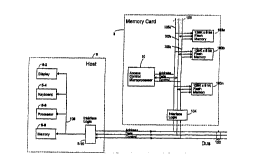
Figure 1 shows an overall block diagram of a system
which ir~L~L~- 3 the memory card ao.. i~LueLed according
to the present invention.
Figure 2 shows in greater detail, the access
control l Luce S ,vr (ACP) of Figure 1 inrl--A;n~ a layout
of its non-volatile memory.
Figure 3 shows a ~l~t~ block diagram of a
~Lt~ al-l flash memory of Figure 1 ';fi~d according to
the present imention.
Figures 4 and 5 are ~low charts used to explain the
operation of the memory card of the present invention in
- carrying out various authentication ~LU~ eduL- s.
w0 95/24698
2 1 622~7 ~
--8--
. IU_ OF T~ ~ r" ~ ~ _
Figure 1 is a block diagram of a secure portable
hand-held computing system 1 usable as a personal
computer or as a transaction ~LUC~.. D~)L. System 1
1 nrlU~ C a memory card 3 constructed according to the
present invention which ~ ~ L~; to a host ~Lu~.eCc~ 5
by a bus 102. The host ~LU~_ ur 5 may take the form of
a palm top personal ~, such as the HP 9 5LX
r-ml r ~ . .1 by Hewlett-Packard. The host ~LUU~__JL 5
~ n~ a liguid crystal display (LCD) 5-2, a keyboard
5-4, a mi~;LU~L~I~ C__~IL 5-6, a memory 5-8 and a serial
interface 5-10 all coupled in common to a bus 106. The
memory 5-8 ; nrl l-A~-: a one megabyte read only memory
(ROM) and a 512 Rbyte random access ~emory (RAM).
T_e Cnnn~ct 1 l~n between t_e memory card 3 and host
uue~8uL 5 is esl-Ahl ~2h~ through a DLal~.laL.l bus
i-lL.:Lrace. In the ~L~r~LL~:d . ~'~ , the bus 102
c f to the Personal r _L~- Memory Card
Internation~l Association (PCMCIAI aL~ -Ll. The
i,.LeL~a~e 102 provides a path ~or LLar~..L~:LLing address,
control and data information between host ~LUU___O~ 5
and the memory card system 3 via a DLàndaL~ .L~L~
chip 104 and a memory card bus 105. Each of the ~U8Q8
102, 105 and 106 include a data bus, a control bus and
an address bus and provide cnnti mln~ signal pathDs
t_rough all like buses. For example, bus 105 inrl~
address bus 105a, data bus 105b, and control bus 105c.
The PCMCIA bus D~d~ld~Ld has evolved from a standard
which DU~ ILLD disk emulation on memory cards to a
suL~I-. l ;Ally different DLall.l-L.l which allows random
acces6 to memory data. The memory card of the present
invention provides a protection~t~-hnic[~l~ which DU~yULLD
this new ~, Lal~da~ d by providing rapid access to random
~WO 9~/24698
21 62287
g
memory locations without resort to encryption
t~rhn~ P~. 8y controlling the data paths which carry
the data from the memory array to the host, the memory
card of the present invention ~L.,~e~ ~5 the data without
i --inAj any ti~ --inAj burferinq, decryption or
other serial prorPC~i nj in this pat_.
Typically, a user ~ raL~ system 1 from the
keyboard 5-4 to perform the typical operations such as
spreAA~h~et and database f~lnrtirnA which display
information on display 5-2 and update information stored
in files in ~emory card 3. The host ~L~c~ ,r 5 sends
address inff~rr~ti ~n over bus 102 to retrieve information
and if desired, update5 the information and send~s it,
along with t_e n~ A r y address and control information
back to memory card 3 .
As shown in Figure 1, the memory card 3 of the
present invention in~ an access control pL~ce.-_ ~L
(ACP) 10 coupled to bus 105 and a number (n) of CMOS
flash memory chips 103a through lOjn, each coupled to
bus 105. ACP 10 is typically the same type Or
prOcPsFi nj element as used in the "Smart Card" . The CNOS
flash memories 103a through 103n may take the form of
flash memory chips ~ Arl ,d by Intel Corporation.
For example, they make take the form of the Intel flash
memory chip ~ iAjnAt~cl as Intel 28FOOlBX lM which
1nr~ eight 128RBYTE: Y 8 CMOS flash memories. Thus,
a 4-l~BYl~ flash memory card could include 32 - C~OS
flash memories, that i8 'n' 3 32.
Wogs/24698 21622g7 r ~
--10--
ACCE88 CONT~OI~ 10
Figure 2 sho~.7s in block diagram i~orm, the access
control yLuue~--~L (ACP) 10 o~ the ~L~f~rL7 d . i ~ .
As shown, ACP 10 ;nrl ~ a ~JLUt__' !' non-Yolatile
memory 10-2, a random access memory ~RAII) 10-4, a
mi~Lu~LUcL3s~r 10-6, an interYal counter 10-8 and an
rL__~ block 10-10 ~I e~7, to bus 10~. Non-
Yolatile memory 10-2 ~o~;r~t~ a numi~er of addL. ~'
locations in which to store A~lthnr~tjca~;nn; - tion
and p.u~,. . Xore sr^-;ft~lly, memory locations 10-2a
store one or more po-snnAl identlfication numbers
~PINs), protocol 8, ~ or other ; rlPnt; f ; cati nn
information ~or verifying that the user has acc~ss to
the system, and for identi~ying the blocks in ~lash
a~ 103a through 103n that the user may access in
t; nn to a time interval value uged ~or re-
Atlthont j r~t; on .
Nemory Inr~t;nn~ 10-2 ~ store the key values used
for protecting each of the flash Pa 103a thro~ gh
103n or the codes used to protect the individual block8
of each of the flash memories 103a through 103n.
Memory 1 ncat; nn~ 10-2c store the program
instruction , ~ ~or perf orming the required
authPnt;C~7t;rn nro~at;nn~ and for cl~oAr;ng the sy8tem if
the pre8et r,nn~ltt; nn~ for failure are met. Certain
program instructions enable the user to control the
~etting of the interval comter 10-8 which e5tl~hl; ~ho~
when user ~ ..1; r~tion tak~s, place. The r -
A-7thont;cation interval defines the t~me be~ween
il.L(:L-u~-ions and for sending an illLeLLU~ to t'.~e host
~L~ _ 5 requiring vPr;ftrAt;nn of the u~er's
identity ~y having the user reenter the PIN or other
Ld. The interval counter 10-8 receiYes clock
L ~ L ~ I
_~WO 95124698
~! 2 1 62287
--11--
pulses from the host ~Luce4sol 5 over bus 102 and can be
set by the user according to the work environment. For
example, at home, the user may turn the timer off (i.e.,
set it to a maximum value), or set the time interval to
one hour. ûn an airplane the user may set it for ten
minutes for increased protection. As described herein,
the user is ~L~, L~ed to 1~ ~uine the setting of this
interval at every "power on" thereoy forcing peri~dic
re~ th~n~ i cations to enforce security.
Fr'~ Y~Yn~Tv-o 103~ ~h--oucrh 103n
Figure 3 is a rlPt~ i 1 DCl block diagram of flash
memories 103a through 103n. Only the detailed logic
circuits of memory 103a are shown since memories 103b
through 103n are cu-._LL~_Led i~Pn~ lly to memory 103a.
The flash memory 103a b~ l l y ' ~es two
sect; t~n~, a section -r nt-~l; n; n~ the security access
control circuits of the present invention and another
section c~nt~nin~ the basic or ~La~lda~d logic circuits
of the flash memory.
~-cllritY Acc0~3 Control 8Oction
As seen from Figure 3, the security control
circuits of the present invention include a 32-bit key
register, a 32-bit volatile lock register 33, a 12-bit
delay counter 32, a ~tOI circuit 39, an all ONES
~tect~cl signal circuit 38, a non-volatile lock memory
35, a one-bit non-volatile lock storage enable element
36, a volatile access control memory 43, an access
i f iC~tion allow AND gate 34 and an output OR gate 45
A~ d as shown. It will be noted that this _ection
receives command control signals designated by various
hPv~ lp~ l values (e.g. 31H through 38H) from a command
r~
WO95/24698 2l 62287 - ~
--12--
register 50 included in the basic logic section. These
signals indicate the di~ferent data values of the set of
, nl4c received by the command register 50 from the
ACP lO via data bus 105b. These . ' are an
important aYtan~i~n to the sets of ~ ` normally
u~ed by the flash memory. The standard flash memory
- ' - take the form o~ the r - ~t; 1 i 70d by the
28FOOlBX flash memory. Those ' are described in
the publication entitled, "Memory Products,~ pllhli~:
by Intel Cu.~uL~tion, ~ eL. .~.~d herein. The
used by the present invention are described in Table 1.
Referring to Table 1, the first command shown is a
load lock memory command which is used to initially load
a random number ~ Le~l lock value into non-volatile
lock memory (LM~ 35 in each memory 103a through 103n.
Each memory 103a through 103n may have a different lock
value or the same lock value ~opan~l i n~ on the security
needs of the users. The lock value is loaded into LM 35
through key (K) register 31 under control of the one
bit, non-volatile storage element 36. The reset lock
storage enable command of Table 1 is used to resQt
storage element 36. This ~L.: ..Ls the lock value stored
in LM 35 from being changed since storage element 36
once reset by the reset lock ~torage enable command
25 cannot be set. The non-volatile L.u.. L-.. t~ of LM 35 are
L.~ re--,d to the L register 33 on F--- -u~. It will
be noted that the location or site of lock memory 35 is
design ~ L. For example, memory 35 could ~e
ted as an eYt an~ n to memory array 54.
The load key register command of Table 1 is used to
load the key register 31 and set the delay counter 32.
The de- !L . L delay counter command is used by the ACP
lO to de_L- by one, the content8 of the delay
counter 32. The read allow memory bank and read disable
Wo 95/2 i698 1 ~ "~ I. . J
2 1 62287
--13--
memory bank ~ nric are used by the ACP lO to enable or
disaole access to the different memory blocks of memory
array 54 during loading of the access control memory 43.
S T bl~ 1
Co_~rd Fir~t Bus Cyc~- ~ecomi llus Cyrle
Oper-tior Ad~ir-s- D-t- Op-r-tlor, Ad~re~- D-t-
10 Lo d Lor~ llr~te 31N ~Irit- R~
~le~ry
2~t Lor,i~
15 Stor ~ ENble ~Ir~te 33N R/A R/A
Loe~i Key
Re~i-t~r llrite 32N i~rlt- Key D-t-
Decre~ent De-
20 I-y cOu,te, ~ t~ 35N R/A R/A
l~ee~i-Allo~l lle~rr
ory B-nr l~rit~ IiBA 34N llrlt- tlBA
2S R--~i-Dl--blo
Ihn~ry B~nk llr~te MBA 3BN llrlte IIBA
Load Lock Memory (31H)
This command copies the ~ 5 of the key
register 31 into the non-volatile lock memory 35 if
and only if the lock storage enable 36 output
signal i5 TRUE.
Reset Lock storage Enable (33H)
This command resets the lock storage enable logic
element 36, thus inhibiting loading or l-h~n~ing the
lock storage memory 3 5 .
Load Key Register ( 3 2H)
This command shifts the prior ~ of the key
regis_er 31, one byte (LSB toward MSB) and loads
"Key Value" from ACP 10 into the key register LSB.
Wos5l24698 2 1 6 2287
--14--
Further, it sets the Delay Counter 32 to its
maximum value, e.g., all ONES.
D~UL~ ~ Delay Counter (35H)
This command deuL~ the delay counter 32 by
ONE. The delay counter must equal ZERO to allow
2, ~ se~ reading of the memory array 54.
Read-Allow Memory Bank (34H)
This command sets the bit UULL 7L~ ~l;n~ to the
memory bank address (MBA) in the access control
memory 43 if and only if the access -ifir~tion
allowed signal 37 is TRUE. This allows read access
to the selected bank.
Read-Disable Memory Bank (38H)
This command resets the bit ~ULLe7~ .8in~ to the
memory bank address in the access control memory
43 .
rr~nc~ ring Table 1 in greater detail, it is seen
that Table 1 also shows the bus cycle operations for
each of the added '~. For each command roT~;rin~
two bus cycles, during each first bus cycle, the command
register 50 receives an 8-bit command ~ L~Læd by ACP
10, sent via the data bus 105a of bus 105 and an input
buffer 51. Command register 50 conditions the 8Ql ectecl
logic element to receive ~rom data bus ~OSb, the
information required to execute the command during a
second bus cycle. As indicated, the second bus cycle is
designated not Arpl; CAhl ~ (N/A) since the reset lock
storage enable and deuL~ delay counter '~ need
only one cycle for execution.
~uring normal operation, the ~ register 31 is
loaded with the key value received from memory locations
10-2b by a load key register command and delay counter
32 is set to its maximum value. Delay counter 32 is
WO 95/24698 r~, ~".,, L'Jlll I
21 62287 - --
--15--
decremented to all ZEROS in L~ ,on~e to s~l~ cPc~ive
decrement delay counter, ~ ~ received from the ACP
10 and qenerates a zero count output signal 41 which is
applied as an input to AND 34.
Each delay counter 32 limits the number of tries or
attempts which can be made to access the flash memories
103a through 103n in the case where a thief removes the
chips and places them upon the "outlaw card" and
~LV~, a p~o~;e~.sc,L or PT~ L to repeatedly try to
guess each memory chip's key. Stated differently,
counter 32 ensures that a ~ign~fir~nt number of tries or
attempts must be made in order to gain illegal access to
the flash memories. The key and delay counter sizes are
salecto~ to require such testing to take an u~r- ~ hl e
amount of time.
Nore cpprifi~ ~l ly~ the Key Register 31 stores
approYimately 4 bill}on 1232) different combinations.
In the ~L~feLL~ L, the delay counter 32 is a
twelve-bit counter. Ac~llm; n~ the delay counter 32 is
de~L~ e once each mi~L~,sec~ , it will require 212
or 4 m;ll;~secnn~cl per attempt at gllpcc~;n1 the key value.
The ACP 10, knowing the correct key value, incurs only a
four m;11;~Pcnn~l delay in the initial setup. Random
~LL L ~ to guess the key value will require 231 tries
for a 50% chance of success. This would reS~uire 231 x
212 mi.~ P~ l or 102 days to guess the key value.
This time is s~ fi~iPnt to deter most thieves. of
course, a longer or shorter time could be provided by
modifying the sizes of the key and delay counter 32.
In the case where the memory card of the pr~sent
invention is stolen and is put into an "outlaw host, "
the ACP 10 limits the number of ,ries by the thief to
guess the PIN by known terhniq~lpc. Such tachniqtlPc may
Wo 95l24698 2 t 6 2 2 8 7 ~ c- I--
--16--
include locking access or destroying data if a threshold
of ih-,ULL__L guesses is ~
During an initial authentication operation for
flash memory 103a, a key value is loaded into the 32 bit
K register 31 in Le. ~V~Se to four S~rrD~ ~ive load key
register ~ ' ( i . e ., data bus 105b is a byte wide
bus). Delay counter 32 i8 forced to its maximum count
of (ALL ONE's) and d~vL- L- l by the ACP 10 sending
d~.;L. ~ d~lay counter _ '- on ~llrc P~ive first bus
cycles. When the delay counter 32 is de-_L- :~ ' to
ZERO, it y- .~_LC~t~ the zero count signal 41 which is
applied to one input of AND gate 34.
I~ the key value stored in the R register 31 equals
the lock value stored in the ..VLL.-lJ l;n~ L L. '~tDr 33
indicating that the user provided the proper
i~nti~ir~t;nn to the host ~Lu.esfiv~ 5, then compare
logic 39 applies an equals compare signal 42 to another
input of AND gate 34. This causes AND gate 34 to
generate an access if iration allowed signal 37 at its
output, which ena~les writing to access control memory
43, under the control of ACP 10. This, in turn,
6"~ " ` t 1 y allows the reading of memory array 54 .
The access control memory 43 ~mt:-inl: volatile
storage of one bit for each block/bank of the memory
array 54. 'rhese bits are cleared to ZERO as part of the
flash memory's power up ~, . In ordèr for data to
be r~ad ~rom the ~emory 103a, the bit ~_VLL- l.. ling to
the -~ _ ' memory block must be At logical ONE.
These bits are set by the ACP 10 issuing read-allow
memory bank ir and only if the access
'ifi~ation allowed signal 37 is l~JE.
As shown in Table 1, during the second bus cycle of
the read-allow memory bank command, the three ( 3 ) high
order address bits of the 8D7 DrtP~ memory bank of memory
_ _ _ _ _ _ _ _ _ _ _ . _ _ _ _ _ _ . ... _ .... . _ _ _ _ _ _ .
-- P~ l/L.., L'~ ~ I
V~O 951~4698
2 1 62287
--17--
array 54 are sent over address bus 105c as well as a
repeat of the h~Y;~c;r-l command identi~ier being sent
over the data bus 105a to command register 50. This
results in a ONE being written into the a-llL-J~d bit
location in access control memory 43. In the preferred
L, the read-allow memory bank command seq~n~e
is repeated eight times since the memory array 54 is
organized into eight banks of 16K bytes each. The ACP
10 may restrict access to s~ ct~ banks by issuing a
0 Sf, : of read-disahle memory bank in a
similar manner.
The output of the access control memory 43 of the
present invention is applied as an en~hl in~ input to
output buffer 52 during each flash memory read cycle
when the c ~ L~ of a location o~ any bank of memory
array 54 is being read out. That is, a read cycle may
occur, however, the data read out is inhibited ~rom
passing through output bu~fer 52 in the ahsence of the
L~,~Liate bank's access control memory gating signal.
More Fr~C;1'ir~l1y, in the case of the ~L~Ce:LL~
i - , acc~ss control memory 43 l nrl uA~c eight
individually ~dlL- ~:,able bit storage Dl ~ an input
address 3 to 8-bit decoder c~nnn~ t~d to the input of
each storage element and a 1 to 8 output mult ~ rl ~Y~r
circuit connected to the output of each storage ~l .
The three high order address bits of each address are
decoded and used to select the storage element for the
block whose c-v~ are to be changed. Similarly, the
same three bits are used to select the output of the
storage element for the block containing the flash
memory location being read.
If the lock memory 35 is fully erased, i.e., at ALL
ONES as indicated by the cont~ntC of the L register 33
being at all ONES, then the output bu~fer 52 is always
S.'~_ I
WO95J24698 2~ 62287 ^ ~ - ~
--18--
enabled. That is, when lock register 33 cr~nt~inc nAEL
ONES, " this generates a signal from ALL ONES detector
element 38 to the OR gate 45 to enable the output burfer
52. This effectively places flash memory 103a in non-
s secure mode. ~his allows all of the security logic
circuits of the present invention to be bypassed.
~ence, the same flash memory chip ean be used for both
secure and r~ e__uL~ applications, thus resulting in
pro~ ctirn ~e i~.
Jl~h 21~mor~r P-~ ~ n oai¢ r~ r~-~ t~
As ~hown in Figure 3, ~ueh eireuits inelude a
memory array 54, a eommand register 50, input/output
logic circuits 60, an address latch 56, a write state
machine 61, erase voltage system 62, an output
multir~Y~r 53, a data register 55, input burfer 51,
output buffer 52 and a status register 58, as shown.
The basic logic eireuits of rlash memory 103a as
~ cCllcced above, takes the form of the type of eircuits
included in the fla~;h memory de6ignated aC 28FOOlBX
m~mufactured by Intel Corporation. Since sueh eireuits
are eonv~nt i nn~ l, they will only be deseribed to the
extent n~rG ~ r y . For furt_er information regarding
sueh eireuit~;, L~:fe~ e may be made to pages 3-109
through 3-134 of the pllhl tcatin~ entitled, "Memory
Produets," Order Number 210830, p--hl i-lh~d by Intel
Corporation, dated 1992. As shown in Figure 3, the
flash memory baQie eireuitS reeeive a number of input
signals (A0-A16), address, data signals (D00-D07) and
eontrol signals (CE, WE, OE, PWD and VPP). mese
signals are deseribed below in Table 2.
~ WO 95124698 ~ r - ~
2 1 62287
--19--
Table 2. Signal Descriptions
Symbol Name and Function
A0-A16 ADDRESS INPUTS for memory adl~ .55es.
~d 1- ~ses are i nt~rnA 1 1 y latched during a
write cycle.
DOO-DO7 DATA INPUTS/OUTPUTS: Inputs data and
during memory write cycles; outputs data
during memory and status reAd cycles. The
data pins are active high and float to tri-
state of~ when the chip is ~ a~ ct~ or the
outputs are ~l;aAhl~d. Data is int~rnAlly
latched during a write cycle.
CE CHIP ENABLE: Activates the device ' s control
logic, input bu~_ers, ~r~ and sense
11 f ~ ~~a. OE is active low, OE high
.l~q~ ~ct~ the memory device and reduces power
Lion to standby levels.
PWD P~ : Puts the device in deep p _.'
mode. PWD 8 active low; PWD high gates normal
operation. PWD=VHH allows ~JL~L n~ oI~ the
memory blocks. PWD also loclcs out erase or
write operations when active low, providing
data protection during power transitions.
OE OUTPUT ENA~3LE: Gates the device's outputs
through the data bu~fers during a read cycle.
OE is active low.
Wo 95/24698 r
21 62287
--20--
WE WRITE ENABLE. Controls writes to the command
register and array blocks. WE is active low.
Ad.lr._33~ and data are latched on the rising
edge o~ the WE pulse.
Vpp ERASE/PROGRAM POWER SUPPLY for erasing blocXs
of the array or ~J~u~L_ irg bytes of each
block. Note: With Vpp ~ Vppl llax, memory
cr~ntont~ cannot be altered.
As shown in TablQ 2 , the Chip Enable (CE), Write
Enable ~Lvve~ (WE) and Output Enable (OE) ) signals
are applied to command register 50 and I/O logic 60 from
host ~ 5, via bus 102 and control bus 105b and
are dispersed to control ~F"''~ f i ~d logic blocks . A
p_._L~ (PWD) signal i8 also applied to command
register 50 for enAhl in~ the flash memory to perform the
operations ~p~ 1 f ~ in Table 2 . This signal can be
used to clear the volatile storage -1- of the flash
memory's security control ~ection as desired thereby
Qnforcing user ~ "Li--~Ati~n when normal operation is
again L~ ~_
Generally, the basic logic ~1- of the ~lash
memory operate in the following manner. Information is
stored in memory array 54 via data bus 105a, input
burfer 51 and d~ta register 55 at an all~e~lLQ~ location
of one of the memory blocks ~re/~i ~i od by the address
received by an address logic 56 ~rom address bus 105c.
Information is read from a 13re-tf~d address location of
a bank of memory array 5~ and is sent to host ~.
5 via an output mul~ i rl~Y~r 53, output bur~er 52, data
bus 105a and bus 102. Status register 58 is used for
storing the status o~ the write state machine, the error
~wossl246s8 P~l,~ ll
21 62287
--21--
suspend status, the erase status, the program status and
the Vpp status.
The write state machine 61 controls the block erase
and controls program algorithms. The program/erase
voltage system 62 is used for erasing blocks of the
memory array 54 or the ~tv~L ;n~ bytes of each block
as a fllnr~irn of the level of Vpp (i.e., when Vpp is at
a high level ~L-~yL in~ can take place; if Vpp is at a
low level, memory array 54 fllnrt-iAn~ ~8 a read only
memory).
OF OPl~l~ION
The operation of the secure memory card of the
present invention will now be de6cribed with particular
reference to the flow diagram of Figur~s 4 and 5.
Before describing such operations in detail, the steps
involved in the fAh~ir~ti~n, .__~ 7~tion and operation
of the memory card will first be described.
As a ~ir6t step, at card fahrication, the ACP 10
sets the lock value for each of the memory chips on the
memory card. It does this by loading the key value into
the lock memory of Pigure 3. These values are stored in
the ACP's pLV~V~d non-volatile memory 10-2 (i.e., keys
l-n in Figure 2). The lock storage enable ~ 36
are then set to ZEROs to inhibit further changing or
reading of lock memory ~ . As these ~1 ~ are
nonvolatile, they cannot be changed unless the entire
flash memory chip is cleared.
As a second step, at application ~;ua~ i 7~tion,
since writing is not affected by the protection
functionality, the memory card can then be loaded with
its data or SV~ ILC application. The ACP 10 is then
loaded with information pertaining to the memory's bank
Wo 95/24698 2 1 6 2 2 8 7
--22--
~--ucLu--: and the degrees of protection which are to be
applied to each memory bank.
As a third step, at user ;u~ tion, the user
est ~Ihlichoc parameters ~or the r.c~ and mode o~
5authentication and cpecif{c data required (e.g.,
pPrsnn~l iclontification numbers (PINs)). This
information is stored in the ACP's memory.
As a fourth step, at power on, the "key register",
"access if1ration All~ " signal and "access control
memory" are initi~l ~ 1 80 as to inhibit access to data
or writing to access control memory 43. The first
authentication dialog i8 initiated.
4~t ~irst authentication dialog, the ACP 10, using
the service~ o~ its host ]?lvv_5~. 5~ prompts the user
and receives aU~hDn~io~tion i-- ~ion. Ir
authentication is ~ r~l, no operation is
.fl ; if ~..c ~-rul, the key register of each
memory chip is loaded with the value stored in the ACP ' s
memory. During this operation, the delay counter 32 i8
used to inhibit chip operation for a period o~ time
rollowing loading to make random tries an u~Lv-lu~ ~ive
process. Loading of the key registers causes the
"access ~ f i ~ation allowed" signal to be true in each
chip. The ACP lo then octAhl i choc access by loading the
access control memories according to the stored
information rnnf 1 ~ation .
As a sixth step, at s-~h~Soq~ont auth~n~ tion
dialog, periotlir~l ly, according to the user's
con~iguration, the ACP lO prompts an additional user
authentication (ro~thont ir~tion) . In the event of
failure, the ACP 10 forces all memory chips to their
power on states, thus inhibiting any access to the
memories ' data by clearing the access control memory 43
and clearing the ~ q of the key register 31. Now,
WO 9512~i698 P~ 'or. I
2 1 62287
--23--
- the operation of the system of Figure 1 will be
described with reference to Figures 4 and 5.
First omerati nnc of the Dav
Figure 4 shows in block diagram form, the various
modes of opDr;~tinn Blocks 402 and 401 show the two
startup conditions. In block 402, the user inserts the
memory card 3 in the previously F - - d 1l~ host
~L~a~ur 5. In block 401, the user powers up host
PL~ 6~II 5 with memory card 3 alrendy installed.
In either of the above startup operations, during
block 402, the ACP 10 and its i..L-- r~r~ are ini~Al i -
in a conventinn~l manner, and block 403 clears all of
the ' n ' K registers 31 and the ' n ' access control
memories 43 as part o~ the flash memories 103a through
103n intDrn~l initialization s=~ æ. This yLe~ Ld
any data from being read out of memories 103a through
103n since output buffer 52, in each memory, is
h3 ~A . The lock value is loaded into the ' n ' L
registers 33 from the I-_- L-_- I ive L~s 35 as a result of
power on.
Now in block 404, ACP 10 sends an interrupt signal
to host I~L~_ 5 which ~ c by requesting the PIN
or other identifying; e Lion from the user. In
block 405, ACP 10, by means o~ the program stored in
memory locations 10-2a, checks that the PIN or other
identifying information matches the information stored
in memory locations 10-2a. Ir no match, then A ,DC; ~; nn
block 406 counts an error and ACP 10 ,h,r~.. 7.~ to block
404 to repeat the test. If the test fails a preset
number of times, then A~ icinn block 406 bL. ~ I r5 to
block 407 to cause ACP 10 to either lock up or destroy
the /-On~Dn~c of the memories 103a through 103n.
W095l24698 2 l 62287
--24--
Fi rst User Authentication Successflll
If in ,laril:irn block 406 there is a match
in~iratin; a . ~ec~r l authentication then in block
408, the ACP 10 via a load key register command loads
esch }~ register 31 from memory locations 10-2b with the
appropriate key value. Also block 409 ~t p~_Ledly
dc_r~ the c ~ l c of delay counter 32 issuing
8~ rP~ive the dL_L- delay counter toward a
binary zero count which causes the generation of the
lo zero count signal 41 in Figure 3.
In block 410, each access control memory 43
location is ioaded with information by mesns of the
read-allow memory bank command to allow access to the
-1 t~-' banks of the ~;ULL' "~.\.lin; ~lagh memory 103a
through 103n.
Int Prm i ttent Re--authPnticA t; rn
In block 411, the ACP 10 awaits the end of the
preset time interval e8t~hl ich~rl by information stor~d
in memory locations 10-2a si~llPd by interval counter
10-8 before reyuesting user re-authentication. Then, in
block 412, the ACP 10 i~ LL~Ls the host pLU~ L 5 to
reyuest the user to L-_ _..Le~ the PIN or other re~uired
nt i f i ~ ~tion.
~eri ~ion block 413 checks the PIN or other
information received ~rom the host ~LI 5 against
the information stored in memory locations 10-2a and the
interval timer 10-8 output is L~._uLd~d. The user has a
preset time interval of typically 30 seconds in which to
enter the AllthPnt-ir~tion information into host pLUU~ ~SUL
5. While the clock is running, if the dpri~ion block
413 test fails, then block 414 records the test as an
error. At that time, it checXs if a maximum nurber of
errors was received and ~ to repeat blocks 412
_ _ _ _ _ _ _ _ _ _ _ _ _ _ _ _ _ _ _ _ _
r ~
~Wo 95/2~698
21 62287
--25--
and 413. If the number of errors equals the maximum
- number, then in block 415, APC 10 clears the flash
memory K register 31 by means of s~ cive load key
register n-lc~ and clears t_e access control
memories 43 with ~ A~ive read-disable memory
-` . Block 415 then ~~ '7 to block 404 to allow
a new "First Authentication" op~ra~ ion to take place.
If the test in rl~ci ~ n block 413 is ~ c-f rul,
the K register 31 remains ~ j !t' (i.e., -rn~inC the
key value previously loaded by the ACP) ~nAhl i nq the
user to Cnnt- i n--e to operate the system 1. In the event
that the 30 seconds elapsed without ~ ci Aion block 413
receiving the PIN or other infnr~ n, the ACP 10
clears the K register 31 and the access control memory
43 as before.
Figure 5 i8 a flow diagram which illustrates how
host ~)LUI~ JL 5 rG~ to an i..LeL~uyt reguest rrOm
APC 10 for authentication in L.~ 6C to blocks 404 and
412 Or Figure 4 . As shown, dQ~i Ainn block 501 is
waiting for an il-Le:LLu~t rrom the ACP 10 requesting that
the user re-enter the PIN or other 1 nforr-t jrn.
Decision block 501 hrAnrh~ to block 502 when it
receives the interrupt from blocks 404 or 412. Block
502 displays the reque8t for t_e PIN or other
information on host display 5-2. Block 503 accepts the
information from the k~ O,Ld and block 504 interrupts
ACP 10. Block 5 sends the PIN to ACP 10.
It will be appreciated by those skilled in the art
that many changes may be made to the ~Lare-L ~d
: i of the present invention without departing
from its t~ hinqc. For example, the invention may be
used with different types of non-volatile memories and
dif f erent interf aces, etc .
W095,24698 21 62287 l~l ~
--26--
While in accordance with the provisions and
statutes there has been illustrated and described the
best form of the invention, certain changes may be made
without departing from the spirit of the invention as
aet forth in the i.r~ Pd claims and that in some cases,
certain ~eal,~L... of the invention may be used to
ad~all~a~- without a "~ U8~1 of other features.
What i6 claimed is:
;