Note: Descriptions are shown in the official language in which they were submitted.
21b~231.5
..
SEI 95-26
TITLE OF THE INVENTION
PHOTOELECTRIC CONVERSION MODULE
BACKGROUND OF THE INVENTION
Field of the Invention
The present invention relates to a photoelectric
conversion module for converting an optical signal into
an electrical signal and, more particularly, to a
photoelectric conversion module which can be mounted on
an optical module as a transmission/reception device
for an optical communication system, or the like.
Related Background Art
As a conventional photoelectric conversion module
of this type, there is a photoelectric conversion
module in which a photodiode (PD) as a light-receiving
element, and a preamplifier for amplifying an
electrical output from this photodiode are mounted on a
TO package. An output from this photoelectric
conversion module, i.e., an output (amplified
electrical signal) from this preamplifier is compared
with a fixed bias by an external comparator. Only a
signal component from which a noise component is
removed is electrically extracted.
SUMMARY OF THE lNv~:NlION
Noise caused by changes in external temperature
and variations in power supply voltage tends to be
superposed on an output from the preamplifier mounted
21~31~
SEI 95-26
on the TO package. According to the present invention,
to remove the influence of noise from an.output
electrical signal amplified by the preamplifier, a
noise compensation output including a component
identical with the noise component is obtained at the
same time when an electrical output is supplied from
the preamplifier. The obtained two types of electrical
outputs (the noise compensation output, and the
electrical output from the preamplifier) are input to a
differential amplifier arranged on the input side of
the comparator to cancel noise superposed on the
electrical output from the preamplifier. With this
arrangement, only a signal component from which noise
caused by changes in temperature and variations in
power supply voltage is removed can be extracted. In
manufacturing a photoelectric conversion module with
such a noise compensation output, the manufacturing
cost, quality, and the like must be sufficiently taken
into consideration so as to put the photoelectric
conversion module into practical use.
More specifically, as shown in Figs. 1 and 4, in a
photoelectric conversion module according to the
present invention, a plurality of circuit constituent
elements are mounted on a package base 10 (TO package)
having a conductive base 31. This conductive base 31
has a plurality of through holes 32 to 35 extending
2162315
.
SEI 95-26
from a first surface 31a of the conductive base 31 to a
.second surface 31b opposite to the first surface. A
light-receiving element 1 for converting an optical
signal into an electrical signal, the light-receiving
S element 1 having a cathode la set at a predetermined
potential (Vp~,), and an anode lb electrically connected
to the conductive base 31; a preamplifier 4 (first
amplifier) having an input terminal 4a electrically
connected to the cathode la of the light-receiving
element 1; an equivalent capacitor S having a first
electrode Sa electrically connected to the cathode la
of the light-receiving element 1, the capacitor 5
having a capacitance value substantially equal to a
capacitance of the light-receiving element l; and a
lS dummy preamplifier 6 (second amplifier) having the same
circuit arrangement as that of the preamplifier 4, the
dummy preamplifier 6 having an input terminal 6a
electrically connected to a second electrode 5b of the
equivalent capacitor S are arranged on the first
surface of the conductive base 31.
The photoelectric conversion module according to
the present invention comprises five lead pins 36 to 40
extending outside the module from the second surface
side of the conductive base 31 of the TO package 10.
In particular, the first lead pin 36 extends through
the through hole 32 of the conductive base 31 from the
~16231~
SEI 95-26
second surface 31b side of the conductive base 31 to
the first surface 31a side without being brought into
contact with the conductive base 31. The distal end of
the first lead pin 36 is electrically connected to an
output terminal 4b of the preamplifier 4. The second
lead pin 37 extends through the through hole 33 of the
conductive base 31 from the second surface 31b side of
the conductive base 31 to the first surface 31a side
without being brought into contact with the conductive
base 31. The distal end of the second lead pin 37 is
electrically connected to an output terminal 6b of the
dummy preamplifier 6. The third lead pin 38 extends
through the through hole 34 of the conductive base 31
from the second surface 31b side of the conductive base
31 to the first surface 31a side without being brought
into contact with the conductive base 31. The distal
end of the third lead pin 38 is electrically connected
to a positive voltage input terminal 9 of the
preamplifier and the dummy preamplifier. The fourth
lead pin 39 extends through the through hole 35 of the
conductive base 31 from the second surface 31b side of
the conductive base 31 to the first surface 31a side
without being brought into contact with the conductive
base 31. The distal end of the fourth lead pin 39 is
electrically connected to the cathode la of the
light-receiving element 1. The fifth lead pin 40 is in
216~315
SEI 9S-26
direct contact with the second surface 31b of the
conductive base 31 and grounded.
The first to fourth lead pins are arranged at an
equal interval so as to surround the fifth lead pin
(ground terminal). An interval between the fifth lead
pin 40 and each of the first to fourth lead pins 36 to
39 is 1.27 mm. The T0 package is preferably a T018
package.
As shown in Figs. 4 and 7, the equivalent
capacitor 5 comprises: an insulating film 62 having a
first surface and a second surface opposite to the
first surface; a common electrode 630 arranged on the
first surface of the insulating film 62; and a
plurality of isolated electrodes 63a to 63d arranged on
the second surface of the insulating film 62. As shown
in Fig. 8, the isolated electrodes 63a to 63d are
electrically isolated from each other and have areas
different from each other. Note that it is preferable
that the equivalent capacitor 5 be a MIS capacitor.
The photoelectric conversion module according to
the present invention further comprises a bias circuit
2 for the light-receiving element 1 between the cathode
la of the light-receiving element 1 and a power supply
terminal 3 (the power supply terminal for the
light-receiving element 1 bonded to the second lead pin
37 through a wire). The bias circuit 2 consists of an
216231~
SEI 95-26
RC network filter. In particular, as shown in Figs. 1
and 9, this RC network filter comprises a MIM aapacitor
constituted by an insulator 52 having a first surface
52b and a second surface 52a opposite to the first
surface 52b, and metal films 53 and 57 formed on the
first and second surfaces 52b and 52a of the insulator
52, respectively, and a resistor 56 formed on any one
of the first and second surfaces 52b and 52a of the
insulator 52.
Noise identical to that of an output from the
preamplifier connected to the light-receiving element
is superposed on an output (noise compensation output)
from the dummy preamplifier whose input terminal is
connected to the equivalent capacitor having a
capacitance value substantially equal to the
capacitance of the light-receiving element. Therefore,
a signal from which the noise is completely removed can
be obtained by a differential amplifier connected to
the input of an external comparator.
The present invention will be more fully
understood from the detailed description given
hereinbelow and the accompanying drawings, which are
given by way of illustration only and are not to be
considered as limiting the present invention.
Further scope of applicability of the present
invention will become apparent from the detailed
2 1 6 2 3 1 ~
SEI 95-26
description given hereinafter. However, it should be
understood that the detailed description and specific
examples, while indicating preferred embodiments of the
invention, are given by way of illustration only, since
various changes and modifications within the spirit and
scope of the invention will be apparent to those
skilled in the art from this detailed description.
BRIEF DESCRIPTION OF THE DRAWINGS
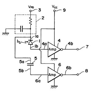
Fig. 1 is a circuit diagram showing an example of
the arrangement of a circuit mounted on a TO package of
a photoelectric conversion module according to the
present invention;
Fig. 2 is a circuit diagram showing an example of
the arrangement of a preamplifier (first amplifier) and
a dummy preamplifier (second amplifier) shown in Fig. 1
~the preamplifier and the dummy preamplifier have the
same circuit arrangement);
Fig. 3 is a view showing a differential amplifier
electrically connected to the electrical output
terminals of the circuit shown in Fig. 1;
Fig. 4 is a perspective view showing the internal
arrangement of the photoelectric conversion module
according to the present invention;
Fig. 5 is a partially sectional view showing the
arrangement of the photoelectric conversion module
according to the present invention;
2162~15
SEI 95-26
Fig. 6 shows views of the arrangement of the TO
package applied to the photoelectr.ic conversion module
shown in Fig. 4, in which the upper view is a plan view
showing the upper portion of the TO package, and the
lower view is a sectional view showing the TO package
along the line B - B in the upper view.
Fig. 7 is a sectional view showing the structure
of an equivalent capacitor along the line A - A in
Fig. 4 and the line C - C in Fig. 8;
Fig. 8 is a plan view showing the upper portion of
the structure of the equivalent capacitor;
Fig. 9 is a perspective view showing the structure
of a bias circuit applied to the photoelectric
conversion module according to the present invention;
Fig. 10 is a circuit diagram showing the
equivalent circuit of the bias circuit shown in Fig. 9;
Fig. 11 is a plan view showing a distributed
capacity low-pass RC network filter as another example
for the bias circuit applied to the photoelectric
conversion module according to the present invention;
and
Fig. 12 is a circuit diagram showing the
equivalent circuit of the bias circuit shown in
Fig. 11.
DESCRIPTION OF THE PREFERRED EMBODIMENT
An embodiment of a photoelectric conversion module
21~231.~
._
SEI 95-26
according to the present invention will be described
with reference to Figs. 1 to 12. Fig. 1 shows a
circuit mounted on a TO package (package base) of the
photoelectric conversion module according to the
present invention. In this circuit, a cathode la of a
photodiode 1 as a light-receiving element is connected
to an input terminal 3 of a photodiode power supply Vpl,
through a bias circuit 2. The bias circuit 2 consists
of an RC network filter constituted by a resistor and a
capacitor. An anode lb of the photodiode 1 is
connected to an input terminal 4a of a preamplifier 4
(first amplifier). A capacitor 5 is an equivalent
capacitor having a capacitance value equal to the
capacitance of the photodiode 1. One electrode 5a of
the capacitor 5 is connected to the cathode la of the
photodiode 1, and the other electrode 5b is connected
to an input terminal 6a of a preamplifier 6. Although
the preamplifier 6 has the same arrangement as that of
the preamplifier 4, the preamplifier 6 does not amplify
a signal component. For this reason, the preamplifier
6 is called a dummy preamplifier. Output terminals 4b
and 6b of the preamplifier 4 and the dummy preamplifier
6 are connected to first and second output terminals 7
and 8, respectively. The preamplifier 4 and the dummy
preamplifier 6 are driven by a power supply Vcc
different from the photodiode power supply. A power
216~31S
SEI 95-26
supply terminal 9 serves as a power supply vcc input
terminal.
Fig. 2 shows a general circuit arrangement of the
preamplifier 4. The dummy preamplifier 6 has the same
arrangement. The reason is that the dummy preamplifier
6 is not used as a preamplifier, but the dummy
preamplifier 6 obtains the same output operating point
as that of the preamplifier 4. Outputs from the two
amplifiers having the same circuit arrangement are
supplied as two inputs (V~ and Vjn23 to an external
differential amplifier 600. With this arrangement, a
common mode component of differential inputs can be
eliminated regardless of variations in power supply
(Fig. 3). In Fig. 2, reference numeric 401 denotes a
FET (field effect transistor), and reference numeric
402 denotes a level shift diode. Furthermore, in this
figure, reference symbols Z1-Z4 denote impedance of the
circuit.
In Fig.3, note that two outputs (VO~T1 and VO~T2 )
from the differential amplifier 600 are input to a
comparator connected to the output of the differential
amplifier 600. Only a signal component is extracted.
The arrangement of an external circuit including the
differential amplifier and the comparator is
well-known.
As shown in Fig. 4, the circuit having the above
- ~ 21GZ~15
SEI 95-26
arrangement is entirely mounted on one TO package 10.
The resultant structure constitutes a photoelectric
conversion module, as shown in Fig. 5. This TO package
10 has a TO18 structure of a TO package standard. As
shown in Figs. 5 and 6, four openings 32 to 35 are
formed at an element mounting portion of a disk-like
conductive base 31. Lead pins 36 to 39 are
respectively fitted and fixed in the openings 32 to 35,
while being insulated from the base plate 31. The TO
package is filled with glass 41. The first to fourth
lead pins 36 to 39 are fixed to and insulated from the
base plate 31 of the TO package by this glass 41. A
fifth lead pin 40 is fixed at the central portion of
the second surface 31b of the element mounting portion
by welding. The lead pin 40 is surrounded by the lead
pins 36 to 39 arranged at an equal interval. An outer
lead length L of each of the lead pins 36 to 40 is 1.5
mm. A pitch P between the central lead pin 40 and each
of the remaining lead pins 36 to 39 is 1.27 mm. with
this arrangement, the lead pins can be easily mounted
on a board, and a commercially available connector
socket can be utilized, thereby easily performing a
drive test.
As shown in Fig. 4, the first lead pin 36 extends
through the through hole 32 of the conductive base 31
from the second surface 31b side of the conductive base
216231~
SEI 95-26
31 to the first surface 31a side without being brought
into contact with the conductive base 31. ~he distal
end of the first lead pin 36 is bonded to the terminal
7 for obtaining an output from the preamplifier 4
S through a wire (reference symbol w denotes a wire in
Fig. 4). The second lead pin 37 extends through the
through hole 33 of the conductive base 31 from the
second surface 31b side of the conductive base 31 to
the first surface 31a side without being brought into
contact with the conductive base 31. The distal end of
the second lead pin 37 is bonded through a wire to the
terminal 8 for obtaining an output from the dummy
ampllfier 6. The third lead pin 38 extends through the
through hole 34 of the conductive base 31 from the
second surface 3lb side of the conductive base 31 to
the first surface 31a side without being brought into
contact with the conductive base 31. The distal end of
the third lead pin 38 is bonded through a wire to a
positive voltage input terminal 9 for applying a
predetermined voltage (Vcc) to the preamplifier 4 and
the dummy preamplifier 6. The fourth lead pin 39
extends through the through hole 35 of the conductive
base 31 from the second surface 31b side of the
conductive base 31 to the first surface 31a side
without being brought into contact with the conductive
base 31. The distal end of the fourth lead pin 39 is
2162315
. ..
SEI 95-26
bonded through a wire to the power supply terminal 3
for applying a predetermined voltage (VPD) to the
cathode la of the photodiode 1. The fifth lead pin 40
is in direct contact with the second surface 31b of the
S conductive base 31 and grounded.
As shown in Fig. 4, a functional board 52 on which
the photodiode 1 and the equivalent capacitor 5 are
mounted, and an IC chip 50 including the preamplifier 4
and the dummy preamplifier 6 are soldered to the
element mounting portion of the conductive base 31.
The functional board 52 is an insulating board. A
thick or thin metal film 57 is entirely formed on a
second surface 52a of the functional board 52, as shown
in Fig. 9. Similarly, thick or thin metal films S3,
lS 54, and 55 are formed in three divided regions on a
first surface 52b of the functional board 52.
A meandrous resistor 56 is formed between the
metal films 53 and 54 by printing or the like (Figs. 4
and 9). The resistor 56, and a capacitor constituted
by the metal films 53 and 54 and the metal film (the
base plate 31 in this embodiment) on the second surface
constitute the bias circuit or RC network filter 2
shown in Fig. 1.
The cathode la of the photodiode 1 and one
2S electrode Sa of the equivalent capacitor 5 are soldered
to the central metal film 54. The equivalent capacitor
216231S
SEI 95-26
5 is a compensation capacity selective MIS (Metal
Insulator Semiconductor) capacitor chip. Fig. ? shows
the sectional structure of the equivalent capacitor 5.
Note that Fig. 7 is a sectional view of the capacitor 5
along the line A - A in Fig. 4 and the line C - C in
Fig. 8. As is apparent from Fig. 7, an insulating film
62 consisting of, e.g., SiO2 is formed on a heavily
doped n- or p-type semiconductor substrate 61. Four
metal electrodes 63a to 63d are formed on the
insulating film 62 (note that only the metal electrodes
63a and 63b are illustrated in Fig. 7). As shown in
Fig. 8, the four metal electrodes 63a to 63d have
different areas, so that a different capacitance value
can be selected by alternatively selecting any one of
the four metal electrodes 63a to 63d.
The TO package 10 having such an arrangement is
covered with a cap 100 having a condenser lens 101 to
complete the photoelectric conversion module of this
embodiment (Fig. 5). Signal light incident from the
outside of the cap 100 is condensed by the condenser
lens 101 and reaches the light-receiving surface of the
photodiode 1. The optical signal is converted into an
electrical signal and input to the preamplifier 4
formed on the IC chip 50. An output signal from the
preamplifier 4 is extracted from the lead pin 36. The
power supply voltage Vp~ is applied to the equivalent
216~315
SEI 95-26
capacitor 5 and the photodiode 1 through the bias
circuit 2. The dummy preamplifier 6 having the same
circuit arrangement as that of the preamplifier 4 is
formed on the single chip (see Fig. 2). Therefore, a
compensation signal having DC and noise components
identical with those of the output signal from the
preamplifier 4 is extracted from the lead pin 37
electrically connected to the output terminal 6b of the
dummy preamplifier 6. The next differential input
amplifier 600 (Fig. 3) cancels the output signal from
the lead pin 36 with the noise compensation signal from
the lead pin 37 to completely remove the noise included
in the output signal from the preamplifier 4.
Note that, it can be technically-considered that a
dummy photodiode having the same structure as that of
the photodiode 1 is used instead of the equivalent
capacitor 5. The dummy photodiode, however, is
expensive. It can also be considered that the input
terminal of the dummy preamplifier 6 is released
without using the equivalent capacitor 5. In this
case, however, a balance may be lost in an RF range.
The equivalent capacitor 5 of this embodiment is a
capacity selective MIS capacitor whose capacitance can
be selected from four capacitance values, as described
above. This capacitor is convenient because the
nearest capacitance value to that of the photodiode 1
216~315
~ .
SEI 95-26
can be selected for this capacitor in mounting even if
the photodiodes 1 vary in manufacturing.
Alternatively, a general MIS capacitor may be used
instead of the capacity selective MIS capacitor, as a
S matter of course. Further, a MIM (Metal Insulation
Metal) capacitor may be used in place of the MIS
capacitor. An on-chip capacitor may be arranged on the
IC chip 50 and defined as the equivalent capacitor 5.
The bias circuit 2 of this embodiment, whose shape
and equivalent circuit are shown in Figs. 9 and 10,
- consists of the RC network filter constituted by the
meandrous film resistor 56 and MIM capacitors 65 and 66
using the corresponding metal films 53 and 54 as
electrodes. The form of the bias circuit 2 is not
limited to this, and a distributed capacity low-pass RC
network filter can be used for the bias circuit 2, as
shown in Fig. 11. Fig. 12 shows the equivalent circuit
of this distributed capacity low-pass filter. In
Fig. 11, reference numeral 71 denotes a film resistor,
and the remaining elements are the same as in Fig. 9.
The bias circuit 2 of any one of the types shown in
Figs. 9 and 11 can have an arrangement smaller than
that of a bias circuit using a dye cap and a wiring
resistor.
As has been described above, according to the
present invention, the light-receiving element for
~16231~
SEI 95-26
converting an optical signal into an electrical signal,
the preamplifier for amplifying an output signal from
this light-receiving element, the dummy preamplifier
having the same arrangement as that of the
preamplifier, and the equivalent capacitor having one
terminal connected to the input terminal of this dummy
preamplifier and a capacitance value equal to the
capacitance of the light-receiving element are mounted
on the TO package. With this structure, the
photoelectric conversion module in which a noise
compensation output can be obtained in addition to a
signal output can be supplied at low cost.
From the invention thus described, it will be
obvious that the invention may be varied in many ways.
Such variations are not to be regarded as a departure
from the spirit and scope of the invention, and all
such modifications as would be obvious to one skilled
in the art are intended for inclusion within the scope
of the following claims.
The basic Japanese Application No. 273555/1994 (6-
273555) filed on November 8, 1994, is hereby
incorporated by reference.