Note: Descriptions are shown in the official language in which they were submitted.
CA 02162347 1998-0~-28
,_
- 1 -
Method and Apparatus For High-Speed Scanning of
Electromagnetic Field Levels
FIELD OF THE INVENTION
The present invention relates to a method of and apparatus for
high-speed scanning of printed electromagnetic field levels and is
particularly concerned with testing circuit packages and like devices.
BACKGROUND OF THE INVENTION
An important tool in circuit board design is the ability to easily and
accurately locate and measure electromagnetic emissions from an
operating circuit board. The prior art electronic emission monitors are
represented by Canadian Letters Patent 1,286,724 assigned to Northern
Telecom Limited, granted on July 23, 1991; United States Letters Patent
4,829,238 granted on May 9, 1989; United States Letters Patent
5,006,788 granted on April 9, 1991; and, United States Letters Patent
5,218,294. These patents describe a method and apparatus for
monitoring electromagnetic emission levels from operating printed circuit
boards.
The prior art enabled the user to carry out two types of scans:
spectral, that is, signal strength relative to the frequency of the scanner,
and spatial, that is, signal strength relative to the position of the signal on
the printed circuit board. The spectral scan retains only the highest value
observed at each frequency point, regardless of the probe, and the display
is, therefore, merely a profile of peak electromagnetic amplitudes plotted
against frequency. All other readings are discarded. A spatial scan takes
a reading of the signal level at the designated frequency, for each probe
within the selected scan area. The scan results are retained in a display
file which provides a colour coded map of the current flows (signal
strength) in the scan area at the defined frequency. The amount of time
required to complete the scan is in the range of 95 seconds.
CA 02162347 1998-0~-28
:'
The disadvantages and limitations associated with the prior art
apparatus relate to the fact that it cannot scan the board under test fast
enough for use in production line testing. To be effective in such an
application requires an method and apparatus for gathering spectral
5 information from all locations of the printed circuit board under test in
much less than one second.
SUMMARY OF THE INVENTION
An object of the present invention is to provide an improved
10 method and apparatus for monitoring electromagnetic field levels from
printed circuit board.
In accordance with an aspect of the present invention there is
provided an apparatus for testing a device for electromagnetic field
therefrom, the apparatus comprising: probe means positionable in a
15 plurality of predetermined positions immediately adjacent to the device,
said predetermined positions having a known spatial arrangement;
addressing means for successively addressing the probe means at each
predetermined position; a receiver connected to said addressing means for
measuring current induced in the probe means by electromagnetic field
20 from respective immediate adjacent regions of the device under test;
signal processing means for analyzing electrical outputs from the probe
means to obtain a measure of electromagnetic field levels immediately
adjacent the device under test associated with each predetermined
position; spectrum analyzer means to gather and analyze spectral
25 information; digital computing means to convert the analog output of the
spectrum analyzer means to a digital output; calibration means to calibrate
the digital output.
In a further embodiment of the present invention, the spectrum
analyzer output is connected to an analog to digital converter via the
30 "video out" output socket.
CA 02162347 1998-0~-28
In yet another embodiment of the present invention, the initial
analog to digital conversion is triggered to start the sweep of the printed
circuit board under test by the electromagnetic scanning apparatus
thereby synchronizing the operation of the device under test with the
5 scanning apparatus allowing the collection of scanning data with respect
to time.
In an embodiment of the present invention, a spectral scan of the
device under test is obtained resulting in a display of the profile of peak
amplitudes plotted against frequency. Several peaks are chosen by the
10 computer system and the frequency of each peak is recorded. From the
frequencies of these peaks, a piece wise linear frequency calibration curve
is produced.
Another aspect of this invention is directed to a method of high-
15 speed scanning of electromagnetic field levels comprising the steps of:placing a device under test immediately adjacent to a probe means which
comprising a plurality of probes, each probe having a predetermined
position within the probe means; addressing a first probe of the plurality
of probes, then synchronizing a spectrum analysis sweep to commence at
20 the same point in time of the activity of the device under test; measuring
electromagnetic field levels from the device under test as detected by the
first probe, and, using a spectrum analyzer, sweep across a desired
frequency range generating a video output signal; digitizing this video
output signal, level calibrating the digitized video output signal and saving
25 the individual data so obtained. Furthermore, these steps can be
optionally repeated for each probe of the plurality of probes as required
and the steps between the individual data of the digitized data set
frequency calibrated, and optionally waiting one sample time more,
followed by repeating the above steps for each possible sample time for
30 each probe of the plurality of probes, and displaying the calibrated data
set.
CA 02162347 1998-0~-28
. - ' ', '
In another embodiment of the present invention a method is
provided whereby measured level of electromagnetic radiation from the
device under test is calibrated. The "Cal Out" output of the spectrum
analyzer is serially connected via an attenuating means of 40dB to the
5 spectrum analyzer input.
Particularly for testing a device for electromagnetic field therefrom,
the apparatus can further include a memory at which circuit layout design
data is stored, and means for inputting said circuit layout design data to
the controller means, said controller means being operable to generate a
10 circuit layout map from the circuit layout design data and said display
being means operable simultaneously to display said map of
electromagnetic field level measures and said circuit layout with said maps
superimposed .
In accordance with the present invention, a spectral analyzer is
15 placed in series with the electromagnetic probe array.
In accordance with another embodiment of the invention, the
"video out" terminal of the spectral analyzer is connected to a high speed
analog to digital (A/D) converter.
By using a spectral-spatial scan, the present invention seeks to
20 overcome the disadvantages found in the prior art. The use of a spectral-
spatial scan makes it possible to measure electromagnetic fields from
devices under test orders of magnitude faster than prior art scanner
apparatus. The increased scanning speeds enable the user to build large
data structures of scan data. In addition, the systems provide powerful
25 manipulative, comparative and analytical tools which allows multiple
perspectives of the scan results, thus establishing a new level of
visualization capabilities.
A further objective of the present invention is to provide a device of
the character herewithin described which permits the production of
30 improved products; significantly reduces pre-compliance times with a
consequent reduction in the time to market of the device under test;
CA 02162347 1998-0~-28
reduced re-engineering or modification costs; cost effective means for
ensuring on-going electromagnetic field compliance with preset standards;
and, minimized life-cycle costs for the product. The spectral-spatial scan
system provide a low cost, automated, non-contacting, testing of a
devices quality and a testing of their performance on the manufacturing
llne.
BRIEF DESCRIPTION OF DRAWINGS
The present invention will be further understood from the following
description with references to the drawings in which:
Fig. 1 illustrates known art scanning apparatus;
Fig. 2 illustrates, in a block diagram, a high-speed scanning
apparatus in accordance with an embodiment of the present invention;
Fig. 3 illustrates in a flow chart a calibration method in accordance
with an embodiment of the present invention;
Fig. 4 graphically illustrates the amplitude verses frequency
spectrum collected by the apparatus of Fig. 2 with a window
superimposed upon a peak in the spectrum in accordance with the method
of Fig. 3;
Fig. 5 graphically illustrates evaluation of a peak for suitability as a
calibration point in accordance with the method of Fig. 3;
Fig. 6 graphically illustrates narrow span sweep of the peak in
accordance with the method of Fig. 3;
Fig. 7 illustrates a sample piece-wise linearization curve used by the
method of Fig. 3 to calibrate the frequency of the collected spectrum
data;
Fig. 8 illustrates in a flow chart a method of spectrum amplitude
calibration in accordance with an embodiment of the present invention;
Fig. 9 illustrates an apparatus set-up used for the method of Fig. 8;
Fig. 10 graphically illustrates an exemplary amplitude calibration
curve obtained by the method of Fig. 8; and
. .
CA 02162347 1998-0~-28
- 6 -
Fig. 11 graphically illustrates an exemplary time-frequency-level plot
obtained by the method of Chart B.
DETAILED DESCRIPTION
In the known apparatus, as shown in Fig. 1, the method for testing
a device for electromagnetic fields therefrom, the method comprising
positioning an array of electromagnetic field monitoring probes occupying
predetermined positions within the array immediately adjacent to the
device under test, successively addressing the probes to measure
10 detected current induced in the probes by electromagnetic field from
respective immediately adjacent regions of the device under test, and
analyzing electrical outputs from the probes to obtain a position-
dependent measure of electromagnetic fields immediately adjacent to the
device under test.
For example, a co-pending device described in Canadian Patent
Application 2,161,292 has a electromagnetic sweep range of plus one
gigahertz ( + 1 GHz). Using a 100 KHz bandwidth, a minimum of 20,000
readings would be necessary to cover all of the information contained in
the electromagnetic spectrum under analysis. The internal digitizer of the
spectrum analyzer on the prior art apparatus would require 34 separate
sweeps with each sweep taking 100 msec to complete. This speed is not
adequate for high speed production applications. One method to increase
the speed of the spectral scanner is to connect an external high-speed
digitizer. However, the only available output is the "video out" output of
the spectrum analyzer. This output is not calibrated and therefore would
yield inconsistent scanning results.
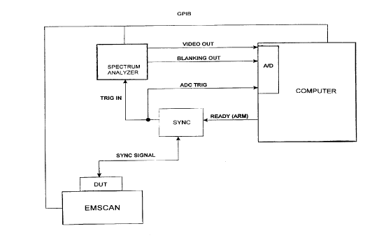
Referring to Fig. 2, there is illustrated in a block diagram, a high-
speed scanning apparatus in accordance with an embodiment of the
present invention. The high-speed scanning apparatus includes an
electromagnetic scanning (EMSCAN) probe array 10, a spectrum analyzer
12, a computer 14 having an analog-to-digital (A/D) converter 16, a
~_,
CA 02162347 1998-0~-28
- 7 -
synchronization (SYNC) block 18 for testing the electromagnetic radiation
emitted by the device under test (DUT) 20. The EMSCAN probe array 10
is connected to the spectrum analyzer 12 and the computer 14 via an
IEEE 488 bus 22. The spectrum analyzer 12 is connected to an A/D
5 connecter via a video out line 24 and a blanking out line 26. The
computer 14 is connected to the SYNC block 18 via a line 28 to provide a
ready or arm signal thereto. The SYNC block 18 has an input/output port
connected to the DUT 20, for receiving from or sending to the DUT 20, a
sync signal via a sync signal line 30. The SYNC block 18 has an output
10 coupled to the spectrum analyzer 12 via a first trigger line 32 and to the
A/D converter 16 via a second trigger line 34.
In operation, a high-speed scan is accomplished by externally
digitizing the video out signal, provided on the video out line 24, in the
A/D converter 16. The digitizing process is initiated in synchronization
15 with the spectrum analyzer. Optionally, the synchronization signal can be
applied to the device under test (DUT) 20 or alternatively, can be received
from the DUT 20. The synchronization is accomplished by the SYNC
block 18. The SYNC block 18 first receives a ready signal form the
computer 14, then in one mode of operation sends a sync signal to the
20 DUT 20 and trigger signals to the spectrum analyzer 12 and A/D
converter 16. Thus, activity in the DUT 20 and both the spectrum
analyzer and the A/D converter are synchronized.
In another mode of operation, the armed SYNC block 18 receives a
synchronization signal, generated by the DUT 20, and in response thereto,
25 sends trigger signals to the spectrum analyzer 12 and the A/D converter
16. The A/D converter 16 uses the video blanking signal from the
spectrum analyzer 12 to stop its digitization process. The spectrum
analyzer, for example, may be a Hewlett-Packard 8594E.
In order to consistently map a predetermined number of data points
30 for each sweep of the spectrum analyzer, data interpolation or decimation
is performed upon the digitized data output from the A/D converter. For
CA 02162347 1998-0~-28
_. , .
example, at a sampling rate of 100 kHz and a sweep time of one second,
each sweep of the spectrum analyzer would provide 100,000 data points.
However, the blanking signal used by the A/D converter 16 to stop
digitizing data likely does not have sufficient accuracy to ensure that
5 precisely 100,000 data points are generated. In this event, the data are
interpolated or decimated such that exactly the predetermined number of
data points or samples result from each sweep.
The step of the high-speed measurement process are summarized in
the following chart:
CHART A
HIGH-SPEED MEASUREMENT PROCESS
Step Process
1. Setup the spectrum analyzer and read back the sweep time.
(Fig. 2)
2. Select the first Emscan probe.
3. Set the "Ready Line" and arm the Synchronizer.
4. The synchronizer waits until the DUT is ready or runs
immediately for unsynchronized scans. The spectrum
analyzer's sweep and the Analog to Digital Converter ~A/D)
are then triggered.
5. The A/D digitizes the signal at the spectrum analyzer's
"Video Out" and "Blanking Out" for a duration of the sweep
time plus a percentage.
6. Determine the end of sweep from the digitized blanking data.
7. Linearly rescale the 'Video Out' data to correct to the number
of digitized points desired.
8. Apply the Level Calibration formula to the data. Note: this
formula is only determined from time to time (once per
month) .
CA 02162347 1998-0~-28
,
_ 9 _
9. Step to the next Emscan probe and repeat step 3-8 until the
last probe is completed. The spectral data for each probe is
stored in an array.
10. Run the Frequency calibration algorithm.
11. Display the data.
Referring to Fig. 3, there is illustrated in a flow chart, a calibration
method in accordance with an embodiment of the present invention.
Once the data has been collected in accordance with steps 1-9 of Chart
A, at step 10, the frequency calibration method of Fig. 3 is applied as
follows. The first step as represented by a block 100 is to find the
10 highest peak in each of several windows, evenly spaced across the
frequency range as illustrated in Fig. 4. Then, as represented by a block
102, based upon a minimum level and the area under the peak evaluate
the peaks in each window for acceptability for use as a calibration point
as illustrated in Fig. 5. Then as represented by a block 104, find the
15 uncalibrated frequency of the first acceptable peak. Then, as represented
by a block 106, set the spectrum analyzer center frequency to that
frequency. Then, as represented by a block 108, set the spectrum
analyzer span to a small percentage of the original span. Then, as
represented by a block 110, take a sweep with the spectrum analyzer.
20 As represented by a block 112, move the spectrum analyzer's marker to
the peak, as illustrated in Fig. 6. In a block 114 determine the frequency
of that marker (peak). At a block 116 repeat from steps 3-8 for each
acceptable peak. Then, as represented by block 118, generate a piece-
wise linearization curve from the measured values, as illustrated in Fig. 7.
25 Finally, as represented by a block 120, use this curve to adjust the
displayed spectrum to the calibrated frequency.
Referring to Fig. 8, there is illustrated, an a flow chart, a method of
spectrum amplitude calibration in accordance with an embodiment of the
present invention. For the apparatus of Fig. 2, at the spectrum analyzer
~,
~ .
CA 02162347 1998-0~-28
,
; '
- 10-
12 attach "Cal Out" to "In" through a 40dB attenuator, as shown in Fig.
6, as represented by a block 200. Set the spectrum analyzer Reference
Level and Attenuation Level so that the trace falls on the bottom graticule,
as represented by a block 202. Measure the voltage on the "Video Out",
5 as represented by a block 204. Increase the spectrum analyzer Reference
Level and Attenuation Level so that the trace falls on the next graticule,
as represented by a block 206. Repeat steps 3 and 4 until the top
graticule has been measured, as represented by a block 208. Calculate a
calibration formula from the data, as represented by a block 210. The
10 formula is a least square fit to a straight line, i.e. Y = aX + b, as
illustrated in Fig. 7.
Once the set-up of Fig. 2 has been calibrated, thereby allowing
high-speed scanning, collection of time related data becomes practical.
There are two methods for collecting time related data: single probe
15 multiple frequency (spectral); and single frequency multiple probes
(spatial).
To gather single frequency multiple probe data, the spectrum
analyzer Center Frequency is set to the desired frequency at zero span
and the output is digitized for each probe for the duration under
20 consideration. The start of the digitization is synchronized to the activity
on the DUT. Detailed steps are given hereinbelow in Chart B.
CA 02162347 1998-0~-28
.; . -
CHART B
SINGLE FREQUENCY SCANNING
Step Process
1. Set up the spectrum analyzer for the desired Center
Frequency, Bandwidths, etc. Set it to zero span and turn
the sweep off.
2. Select the desired probe.
3. Wait for a trigger signal for the DUT.
4. Digitize the 'Video Out' of the spectrum analyzer for the
duration desired and save the data.
5. Select another probe and repeat steps 3-4.
6. Display the data.
To gather single probe spectral data, the spectrum analyzer is setup
for the desired spectrum sweep and a single probe is selected. The
spectrum analyzer sweep is triggered at time 0 of the activity on the DUT
and the data collected. The spectrum analyzer is then triggered at time 0
15 + 1 n sample duration(s) and process is repeated until data has been
collected for the desired time intervals. Note: multiple probes could be
scanned in this fashion to produce a data set of position verses time and
frequency. That is a combination of the two types of scans. Detailed
steps are given hereinbelow in Chart C.
CHART C
SINGLE PROBE TIME SCANNING
Step Process
1. Setup the spectrum analyzer and read back the sweep
time. (Fig. 2)
2. Select an Emscan probe.
3. Set the 'Ready Line' and arm the Synchronizer.
CA 02162347 1998-0~-28
,,_
4. The synchronizer waits until the DUT is ready. The
spectrum analyzer's sweep and the Analog to Digital
Converter (A/D) are then triggered.
5. The A/D digitizes the signal at the spectrum analyzer's
'Video Out' And 'Blanking Out' for a duration of the sweep
time plus a percentage.
6. Determine the end of sweep from the digitized blanking
data.
7. Linearly rescale the 'Video Out' data to correct to the
number of digitized points desired.
8. Apply the Level Calibration formula to the data. Note: this
formula is only determined from time to time (once per
month) .
9. Repeat step 3-8 waiting one sample time more each time
until the desired duration has passed. (Fig. 11) The
spectral data for sample time is stored in an array.
10. Run the Frequency calibration algorithm.
Note: for a combination time scan, select another probe
and repeat steps 2-10 until all the desired probes are
scanned.
11 . Display the data.
Numerous modifications, variations, and adaptations may be made
to the particular embodiments of the invention described above without
departing from the scope of the invention, which is defined in the claims.