Note: Descriptions are shown in the official language in which they were submitted.
ATM CELL FORMAT CONVERTER USING CELL START
INDICATOR FOR GENERATING OUTPUT CELL PULSE
Background of the Invention:
The present invention relates to conversion of
ATM (asynchronous transfer mode) cell format and, in
particular, to solution of timing error in the
conversion.
An ATM cell is a piece of data having a fixed
bit length and comprises a header for containing a
destination address and an information field for
containing information to be transferred. The ATM cell
can be conveniently handled as a data packet.
According to the ITU-TS (International
Telecommunication Union, Telecommunication Standard-
ization Sector), the ATM cell in the user-network
interface comprises the header of 5 bytes and the
information field of 48 bytes, as specified in I.361.
Therefore, the ATM cell has a total of 53 bytes.
Further, an SDH (synchronous digital hierarchy)
frame format is recommended for transferring the ATM
cells, in ITU-TS, I.121.
Since the SDH frame is known in the art, it is
omitted for the purpose of simplification to describe the
SDH frame in detail. However, it is only pointed out
that the SDH frame comprises two portions of a header and
z~ ~z~5~
2
a payload. The header comprises a section over head SOH
and a path overhead POH which are collectively referred
to as SPOH hereinafter. A plurality of ATM cells to be
transmitted are contained in and carried by the payload
through the network.
In user equipments, the ATM cell often has an
extra or redundant byte for a special use. However, the
redundant byte must be removed at the user-network
interface.
Further, in the user's equipments, the SDH frame
is often treated to carry the ATM cells in the SPOH as
well as the payload. The ATM cells carried in the SPOH
must be transferred into the payload.
Accordingly, it will be noted that conversion of
ATM cell format is often required at the user-network
interface.
An ATM cell format converter known in the prior
art uses a memory as a conversion memory. An ATM cell is
separated into a plurality of data blocks which are
written into a plurality of addresses in the conversion
memory, one after another. The writing is started by an
input cell pulse which indicates a start or beginning of
the ATM cell. Then, the data blocks written are read out
from the conversion memory one after another and are
arranged to form a read out ATM cell. A start or
beginning one of the data blocks is determined by an
output cell pulse produced in an external processing
circuit. Therefore, when the output cell pulse
CA 02162351 1999-06-28
3
erroneously becomes out of phase, the read out ATM cell is not
correct and contains data blocks which are part of an adjacent
ATM cell.
Summary of the Invention:
It is an object of the present invention to provide
an ATM cell-format converting device wherein the output cell
pulse can be produced in synchronism with reading out the
beginning one of the data blocks in the ATM cell so as to
remove erroneous taming difference of the output cell pulse
and the beginning data block read out.
According to the present invention, an ATM cell
format converting device is obtained which comprises:
conversion memory means having a plurality of addresses each
having N-bits for temporarily storing an ATM cell so as to
perform ATM cell-format conversion; applying means for
separating the ATM cell into a plurality of data blocks, each
of said plurality of data blocks having M bits, to apply the
data blocks to said conversion memory means; writing address
generating means for generating a plurality of writing
addresses of said conversion memory means for writing each of
said plurality of data blocks to a respective one of said
plurality of writing addresses; writing means for writing each
of said plurality of data blocks to a respective one of said
plurality of writlIlg addresses together with a cell start
indicator, said ce=L1 start indicator being one of a first
indicator for indicating a beginning data block of said
plurality of data blocks and a plurality of second indicators
CA 02162351 1999-06-28
4
for respectively indicating others of said plurality of data
blocks which follow the beginning data block in the ATM cell;
reading address generating means for generating reading
addresses of said conversion memory means for reading out each
of said plurality of data blocks; and reading means for
reading out each of: said plurality of data blocks from the
reading addresses so that said beginning data block is read
out together with :;aid first indicator and so that each of the
others of said plurality of data blocks is read out together
with a respective one of said plurality of second indicators.
According to another aspect of the present
invention, an ATM cell format converting device is obtained
which comprises: conversion memory means having a first
plurality of addre~~ses for temporarily storing an ATM cell so
as to perform the ATM cell-format conversion; an indicator
memory having a second plurality of addresses, corresponding
to the first plurality of addresses in the conversion memory
means, for storing a first indicator for indicating a
beginning position of the ATM cell; applying means for
separating the ATM cell into a plurality of data blocks, each
of said plurality of data blocks having a predetermined number
of bits, to apply t:he data blocks to said conversion memory
means; writing address generating means for generating a
plurality of writing addresses of said conversion memory means
for writing each of: said plurality of data blocks to a
respective one of said plurality of writing addresses; writing
means for writing each of said plurality of data blocks to a
respective one of ~oaid plurality of writing addresses and for
CA 02162351 1999-06-28
writing said first indicator in said indicator memory at one
of said second plurality of addresses corresponding to the
respective one of .said plurality of writing addresses to which
a beginning data block of said plurality of data blocks is
written, with second indicators being written in the indicator
memory at others of said second plurality of addresses, each
of said others of aaid second plurality of addresses
corresponding to a respective one of said plurality of writing
addresses to which each of said others of said plurality of
data blocks which :follow the beginning data block in the ATM
cell are written; :reading address generating means for
generating reading addresses of said conversion memory means
for reading out each of said plurality of data blocks from a
respective one of said reading addresses; and reading means
for reading out each of said plurality of data blocks at the
reading addresses :from said conversion memory means and
reading out said first and second cell start indicators from
said indicator memory from the respective ones of said second
plurality of addresses which correspond to the respective ones
of said reading addresses, so that the beginning data block is
read out together with said first cell start indicator and so
that said others o:f said plurality of data blocks are read out
together with said second cell start indicators.
In those ATM cell format converting devices
described above according to the present invention, the ATM
cell-format conversion performed is a conversion from a state
where ATM cells are held in a header portion and a payload
portion in a SDH frame to another state where the ATM cells
CA 02162351 1999-06-28
5a
are held in the payload portion alone in the SDH frame.
Brief Description of the Drawings:
Fig. 1 i;a a schematic diagram illustrating an ATM
structure;
Fig. 2 i:Llustrates an SDH frame used in a user's
equipment and a converted SDH frame carrying ATM cells;
Fig. 3 is a block diagram illustrating a known ATM
cell format converter;
21b2351
6
Fig. 4 is a view of various signals for writing
ATM cells into a conversion memory in Fig. 3;
Fig. 5 is a view of various signals for reading
ATM cells from the conversion memory in Fig. 3:
Fig. 6 is a block diagram of an ATM cell format
converter according to an embodiment of the present
invention; and
Fig. 7 is a block diagram of another embodiment
of the present invention.
Description of Preferred Embodiments:
Prior to description of preferred embodiments of
the present invention, the prior art will be described
for sake of the better understanding of the present
invention.
Referring to Fig. 1, there is shown a structure
of the ATM cell in the user-network interface as
described in the preamble.
The ATM cell shown therein has a total of 53
bytes and comprises the header of 5 bytes and the
information field of 48 bytes. The redundant byte is
also shown by an imaginary line.
Referring to Fig. 2, a known ATM cell conversion
is illustrated. In detail, the SDH frame 11 in a user's
equipment is shown to carry the ATM cells in the SPOH as
well as the payload. Each of the ATM cells has 54 bytes.
For example, according to the STM-1 (synchronous
transport module-1) frame format, the SDH frame 11 has 9
byte rows, each row having 270 bytes. Accordingly, it
CA 02162351 1999-06-28
7
will be understood that the SDH frame 11 shown has 45 ATM
cells. In the SDH frame 11, each of the 9 byte rows is
shown to have a 4kHz bit length.
At the user-network interface, the ATM cells
carried in the SPOH must be transferred into the payload
by ATM cell fox~nat converter. The converted SDFI frame 12
is shown to have ATM cells in the payload only but not in
the SPOH. Each of the ATM cells has 53 bytes.
Referring to Figs. 3, 4, and 5, an ATM cell
format converter known in the prior art and its operation
will be described for the conversion shown in Fig. 2.
The known ATM cell format converter shown in Fig.
3 therein uses a memory as a conversion memory 21 for
temporarily storing an ATM cell to be converted as a
plurality of data blocks separated each having a
predetermined data bits.
At a writing side of the conversion memory 21,
there are provided a write timing generating circuit 22,
a writing address counter 23, and a writing circuit 24.
The converter receives from an external supply
circuit ATM cells, as input data signal (IDS) to be
converted, one after another, together with an input cell
pulses (ICP) and a write control signal (WCS). The time
relation of these~signals are illustrated in Fig. 4.
Each of the input cell pulses indicates a start
or beginning of each of the ATM cells of the input data
signal. The write control signal is for generating a
timing signal which determines a timing for writing the
2~~23~~
8
input data signal into the conversion memory 21 and for
generating a writing address.
Upon firstly receiving the input cell pulse, the
write timing generating circuit 22 resets the content in
the writing address counter 23. The writing address
counter 23 generates a writing address of "0". When the
writing circuit 24 receives the input data signal and the
writing address of "0", the writing circuit writes a
beginning one (B1) of the data blocks of the ATM cell
into "0" address of the conversion memory 21. There-
after, the write timing generating circuit 22 increments
the content in the writing address counter 23 in response
to subsequent reception of the write control signal.
Thus, the writing circuit 24 writes the subsequent data
blocks of the ATM cell in different addresses in the
conversion memory 21 one after another as shown by B2,
B3, ... Bm in Fig. 4.
It will be noted that a repetition period of the
write control signal is selected to determine a
predetermined bit length of each of the data blocks
written in different addresses in the conversion memory.
Thus, ATM cell is stored in the conversion memory
21 as a plurality of data blocks of the ATM signal.
Then, the stored ATM cell is read out from the
conversion memory 21 to form an output data signal (ODS)
which provides an ATM cell format converted signal.
At a reading side of the conversion memory, there
are a read timing generating circuit 25, a reading
CA 02162351 1999-06-28
9
address counter. and reading circuit 27.
The reading circuit 27 reads the data blocks
stored in the conversion memory 21 in response to reading
addresses delivered from the read timing generating
circuit 26. That is, upon receiving a SDH payload
indication signal (PIS) which indicates the payload
portion of.the converted SDH frame (12 in Fig. 2) and an
output cell pulse (OCP) which indicates a start or
beginning of an ATM cell in the output data signal. The
output data signal is supplied to an external processing
circuit and is ,processed therein into the converted
signal. The external processing circuit supplies the SDH
payload indication signal and the output cell pulse. The
time relation o:f those signals is shown in Fig. 5.
Upon first receiving the SDH payload indication
signal and the output cell signal, the read timing
generating circuit 25 starts control of a read address
counter 26 and periodically delivers thereto read timing
pulses. The reading address counter 26 generates reading
addresses incremented by the read timing pulses from the
read timing generating circuit 25. Thus, the plurality
of data blocks stored in the conversion memory 21 are
read out to provide the output data signal.
Then, subsequent data blocks B1, B2, ... , Bm' in
the output data signal are treated as a converted ATM
signal with B1 as a start one as shown in Fig. 5.
Referring to Fig. 2, considering that
the ATM cell in the converted SDH frame has 53 bytes, it
2162357
1~
is noted that reading of the redundant byte is not
carried out in the reading operation.
The above operation is repeated for subsequent
ATM cells as shown in Figs. 4 and 5. Thus, the converted
SDH frame 12 is obtained.
In the known device, the cell format conversion
can be performed without error if the input and output
cell pulses are supplied with correct timing.
In the known device, the timing of the reading
address is determined by application of the output cell
pulse. Therefore, when application of the output cell
and the beginning data block in the ATM cell are out of
phase with each other as shown by an incorrect output
pulse P and a correct pulse P' shown by a dotted line,
the ATM cell cannot be formed at the reading side, as
shown by cell 3 in Fig. 5. Thereafter, each of the cells
determined by the output cell pulses contains data blocks
in subsequent two adjacent ATM cells, so that the
subsequent conversion cannot provide correctly converted
ATM cells. Accordingly, it has sometimes been caused
that data of one SDH frame unfortunately becomes
meaningless.
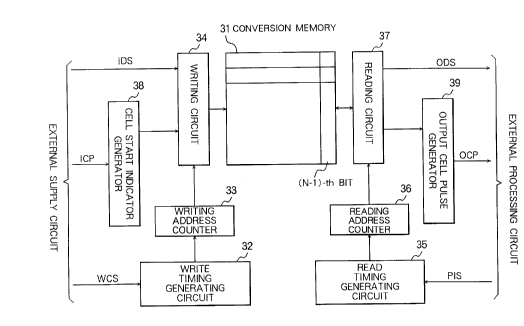
Referring to Fig. 6, an ATM cell format converter
according to an embodiment of the present invention is
shown for performing a conversion from a state where ATM
cells are held in a header portion and payload portion in
a SDH frame (11 in Fig. 2) to a state where the ATM cells
are held in the payload portion alone in the SDH frame
21 b2351
11
(12 in Fig. 2).
The present converter is similar to the known
converter in Fig. 3 except for some differences.
Accordingly, the description of the present converter
will be focused to those differences for the purpose of
simplification.
The present converter comprises a conversion
memory 31, a write timing generating circuit 32, a
writing address counter 33, a writing circuit 34, a read
timing generating circuit 35, a reading address counter
36, and a reading circuit 37 which are corresponding to
blocks 21-27, respectively, in Fig. 3. The present
converter is further provided with a cell start indicator
generator 38 and an output cell pulse generator 39.
The conversion memory 31 is a memory having a
plurality of addresses each having N-bits. The ATM cell
is separated into a plurality of data blocks each having
M bits (M< N). Each of the M-bit data blocks is written
into zeroth through (M-1)-th bits of each address in the
conversion memory 31. The addresses are given from the
writing address counter 33 which is controlled by the
write timing generating circuit 32 in the similar manner
as in Fig. 3. However, the writing address counter 33
only receives the write control signal (WCS) from the
external supply circuit and generates the write timing
signal in response to the write control signal and
increments the writing address counter.
262351
12
The input cell pulse (ICP) is applied to the cell
start indicator generator 38 which generates a one-bit
signal "1" in response to the input cell pulse. However,
the cell start indicator generator 38 keeps its output at
"0" level when the input cell pulse is absent. The
output of the cell start indicator generator 38 is
applied to the writing circuit 34 and is written into
(N-1)-th bit position in one of the addresses in the
conversion memory 31 upon writing operation for one of
the data blocks into the one address by the writing
circuit 34.
Thus, the data blocks of the ATM signal are
stored in the conversion memory 31 together with the cell
start indicator "1" accompanying the start one of the
data blocks of the ATM cell.
The stored data blocks and the cell start
indicator are read out from the conversion memory 31 by
the reading circuit 37 in response to reading addresses
which are given from the reading address counter 36.
Upon receiving the payload indicating signal
(PIS), the read timing generating circuit 35 starts
control of the read address counter 36.
The stored data blocks are read out from
addresses in the conversion memory 31 subsequently
together with the start indicator. Each of the data
blocks read out from zeroth through (M-1)-th bit
positions in each address is delivered as the output data
signal (ODS) to the external processing circuit in the
Zi~23~1
13
similar manner as in Figs. 3 through 5. The cell start
indicator read out from the (N-1)-th bit position in each
of the addresses in the conversion memory 31 is applied
to the output cell pulse generator 39 through the reading
circuit 37. When the indicator is "1", the output cell
pulse generator 39 generates an output cell pulse (OCP).
Accordingly, the external processing circuit
receives the output data signal (ODS) and the output cell
pulse together with the beginning one of the data blocks
of the ATM cell, and can therefore arranges, as a start
data block of the ATM cell, the data block corresponding
to the output cell pulse with the next subsequent output
data blocks following the start data block to form an ATM
cell.
According to the present embodiment, the output
cell pulse indicating the beginning or start data block
of the ATM cell is generated in response to the start
indicator read out from the conversion memory 31 together
with the start data block. Therefore, the. start data
block is always arranged at the beginning of the ATM
cell. This means that the conversion of the ATM cell is
not erroneously performed.
Referring to Fig. 7, an ATM cell format converter
according to another embodiment shown therein is similar
to the converter in Fig. 6 except that another memory 40
is provided for storing the cell start indicator without
use of memory area in the conversion memory 31.
Accordingly, conversion memory is represented by 31' in
2162351
14
Fig. 7.
The cell start indicator from the cell start
indicator generator 38 is written into the indicator
memory 40 by the writing circuit 34. The cell start
indicator stored in the indicator memory 40 is read out
by the reading circuit 37 and delivered to the output
cell pulse generator 39.