Note: Descriptions are shown in the official language in which they were submitted.
W094/29897 216 2 4 9 9 PCT~S94/06387
-- 1 --
METHOD FOR PROVIDING ELECTRICAL
INTERCONNECTIONS B~lw~ ADJACENT CIRCUIT BOARD
LAYERS OF A MULTI-LAYER CIRCUIT BOARD
BACKGROUND OF THE INVENTION
The present invention relates to multi-layer
circuit boards. In particular, the invention relates to
improved electrical interconnections for circuit board
layers of a multi-layer circuit board, and to a method of
10 making those interconnections.
Multi-layer printed circuit boards are known in
the art, and are used to make complex electrical
circuits. (As used herein, a circuit board consists of
a pattern of conductive traces which are used to
15 interconnect electric components. The conductive traces
are bonded to or otherwise incorporated into an
insulating substrate which mechanically supports the
components. This includes single and double sided
boards, multi layer constructions, hybrids, multi-chip
20 modules, chip on board assemblies and the like. The
conductive traces may be formed using any number of
techniques, for example electroplating, etching,
sputtering, mechanical attachment using adhesives and
others. The substrate can be flexible or rigid and can
25 be fabricated of any suitable material, for example
polymers, ceramics, glasses, silicon etc.) Electrical
connections between components of the electrical circuits
are provided on the circuit board layers of the multi-
layer circuit board. Using multiple circuit board layers
30 allows the circuit designer to lay out complex circuit
designs using many components in which those components
require numerous interconnections. Multi-layer circuit
boards increase component density and functionality per
unit volume.
Each circuit board layer of a multi-layer
circuit board carries electrical connections, or
electrical traces, which act as wires and are used to
W094/29897 PCT~S94/06387
~,~6~9~ - 2
interconnect the various components of the circuit.
Electrical connection between adjacent circuit board
layers is achieved using "vias." A via is created by
forming a hole between ad~acent layers. The hole is
5 filled with conductive material to form an electrical
connection between the two adjacent layers.
Typically in printed circuit board (PCB)
fabrication (otherwise known as printed wiring board or
plated through hole technology), the electrical traces
10 are formed separately on each layer of the multi layer
circuit board. The circuit board layers of the multi-
layer circuit board are then stacked and aligned to each
other with an electrically insulating bonding layer
between adjacent layers. The assembled layers are then
15 subjected to heat and pressure to provide a bond between
adjacent layers. Via holes are then drilled in the
appropriate locations which interconnect pads on
successive layers. The electrical interconnect is
achieved by applying a conductive material to the side
20 walls of the via holes. The prior art requires the metal
via contact pads to have sufficient area on the circuit
board to accommodate the drill cross section and/or any
misalignment. These large pad areas limit the component
density of the circuit board. To form buried vias
25 additional processing is required. Namely, the above
structure is treated as a sub-assembly several of which
can be laminated together to form the full board.
The advent of semiconductor processing and
advanced materials has permitted the fabrication of
30 circuit boards on a much finer scale than the printed
circuit boards described above. Examples of these
include hybrids, multi-chip modules (MCMs) and the like. t
Typically, MCMs are manufactured in small numbers of
aerospace, military and supercomputer applications. An
35 example would be MCM-Ds. The D refers to deposition
where a circuit is built up upon an inorganic non-
conducting substrate using thin film approaches with
WOg4/29897 21 6 2 4 9 9 PCT~S94/06387
.
-- 3
copper or aluminum traces and organic or inorganic
dielectrics. Using these technologies a multi layer
circuit is built up by a sequential process. This
technology is capable of fabricating very fine lines and
5 vias (blind, stacked, and buried) resulting in very much
higher circuit densities than traditional plated through
hole technology described above. However, this increased
density comes at the cost of much more expensive
processing which is usually accomplished in sequential
10 batch processing. Batch processing does not lend itself
to high volume production and the sequential fabrication
results in lower yield as the deposition of one defective
layer ruins an entire part.
U.S. Patent 5,046,238 issued September 10, 1991
15 to Daigle et al. entitled METHOD OF MANUFACTURING A
MULTILAYER CIRCUIT BOARD describes a method for providing
interconnections between layers of a multi-layer circuit
board and is hereby incorporated by reference. The
technology is practiced using fluoropolymers which are
20 expensive and are traditionally difficult to process.
Processing difficulties include adhesion problems and the
requirement of high temperatures for processing laminates
(700F and above). In addition, the process is practiced
in batch form which is not easily amendable to high
25 volume production.
SUMMARY OF THE INVENTION
The present invention provides an improved
process for assembling a multi-layer circuit board with
30 an improved wiring density. The invention provides an
improved method of forming interconnections between
adjacent layers in a multi-layer circuit board where
stacked, buried and blind vias which occupy areas smaller
than those occupied by plated through hole technology can
35 be fabricated routinely. The invention does not rely on
high cost low volume fabrication methods such as is
common in the fabrication of MCMs. In addition, a
W094/29897 PCT~S94/06387
~4~ 4 _
parallel process for assembling a multi-layer circuit
board that reduces the number of manufacturing sequences
and increases the yield of completed parts in comparison
to sequential processing is provided. Each circuit board
5 layer is fabricated separately allowing inspection of
each layer prior to incorporation in the final part.
In one embodiment of the invention, a circuit
board layer is formed by depositing electrically
conductive material which forms electrical circuit traces
10 as well as interconnect pads on one side of an
electrically insulating material. The electrically
conductive traces are then exposed on the uncircuitized
side of the circuit board layer by forming holes in the
electrically insulating material at locations where a via
15 is desired.
The interconnection is fabricated by the
formation of rigid bumps of a conductive material in the
holes formed in the electrically insulating material
which protrude above the surface of the electrically
20 insulating material. An electrically conducting metal
which is capable of forming an electrically sound metal
to metal bond between the bump and the corresponding pad
on an adjacent layer is then deposited on the surface of
the bumps or the pads, more frequently on both.
In accordance with another aspect of the
invention, a layer of electrically insulating bonding
material is deposited over at least one of the surfaces
of the circuit board layer fabricated as described above.
A plurality of these layers are then aligned and fused
30 together by the application of heat and pressure in a
single lamination step to form a multi-layer circuit
board. The metal on the surfaces of the bumps bonds with
the metal on the pads providing the electrical
interconnect between layers and the insulating bonding
35 material forms the mechanical bond that holds the layers
together and isolates the via connections.
WO94l29897 2 I 6 2 4 9 9 PCT~S94/06387
.
-- 5
The above fabrication method can be carried out
in a batch process, a continuous process or in a
combination of the two. Fabrication using a continuous
process enables large volume production of the circuit
5 board layers a clear advantage over the batch type
process practiced in both PCB and MCM manufacturing. The
ability to perform the majority of the fabrication in a
continuous process is an important aspect of this
lnvention.
In another embodiment, the circuit board layers
are fabricated in the method described above and
laminated under heat and pressure as described above
however, the insulating bonding material is substituted
with an anisotropically conductive adhesive which by
15 design is an electrical insulator in the plane of the
circuit layer but permits electrical conduction in the
out of plane direction.
BRIEF DESCRIPTION OF THE DRAWINGS
Figure 1 is a side cross sectional view of a
dielectric film circuit board layer.
Figure 2 is a side cross sectional view of the
circuit board layer of Figure 1 including an adhesion and
seed metal layer.
Figure 3 is a side cross sectional view of the
circuit board layer of Figure 2 including patterned
photoresists.
Figure 4 is a side cross sectional view of the
circuit board layer of Figure 3 including a layer of
30 trace metal.
Figure 5 is a side cross sectional view of the
circuit board layer of Figure 4 including a via hole
extending through the circuit board.
Figure 6 is a side cross sectional view of the
35 circuit board layer of Figure 5 following removal of the
photoresist and plating of a solid via.
W094l29897 PCT~S94/06387
2~2~5~ - 6 -
Figure 7 is a side cross sectional view of the
circuit board layer of Figure 6 following removal of the
adhesion and seed metal layer.
Figure 8 is a side cross sectional view of the
5 circuit board layer of Figure 7 following deposition of
a cover metal layer.
Figure 9 is a side cross sectional view of the
circuit board layer of Figure 8 including an adhesive
film and a plurality of spaced apart circuit board
10 layers.
Figure 10 is a side cross sectional view of the
circuit board layers of Figure 9 following lamination to
form a multi-layer circuit board in accordance with the
present invention.
Figure 11 is a side cross sectional view of a
test sample.
DETAILED DESCRIPTION OF THE PREFERRED EMBODIMENTS
Figures 1 through 11 are cross sectional views.
20 For clarity, cross hatching has been omitted.
Figure 1 shows a cross-sectional view of a
circuit board layer 10. In a preferred embodiment,
circuit board layer 10 comprises a precast polymeric
dielectric film. The particular dielectric film used is
25 a matter of choice however, web polyimide is an example
of one that works well. As shown in Figure 2, a
conductive metal layer, and an adhesion layer is
deposited if needed, on the first side of circuit layer
10. The adhesion layer helps bond the metal layer to the
30 dielectric film. The composition of the adhesive layer
is a matter of choice depending on the metal and
dielectric materials used. The outer metal layer portion
of layer 12 can be comprised of copper or other
appropriate conductive metal and can be deposited by any
35 appropriate method. Electrodeposition is one process
that works well. The resulting metal layer 12 acts as a
seed layer for later deposition.
W094/29897 PCT~S94/06387
2I6~4~
-- 7
Next, photoresist 14 is deposited, as shown in
Figure 3. Photoresist 14 is a standard photoresist
deposited on circuit board 10 using conventional
techniques. The photoresist is exposed to radiation
5 through a mask. The photoresist is then developed, which
causes portions of the photoresist to be removed exposing
material and forming a patterned layer 14 as shown in
Figure 3.
After photoresist layer 14 has been patterned,
10 a trace metal layer 16 is deposited on the exposed
adhesion and conductive metal layer 12 as shown in Figure
4. In a preferred embodiment, trace metal layer 16
comprises copper and is deposited through
electrodeposition techniques so that it is only formed on
15 the exposed portions of layer 12. Trace metal layer 16
forms an electrical circuit carried on circuit board
layer 10. Trace metal layer 16 provides the electrical
traces which will interconnect components when they are
placed in the completed multi-layer circuit board.
20 Additionally, the trace metal provides electrical "pads"
which are used to interconnect adjacent circuit board
layers. The above discussion of circuitization of the
dielectric illustrates one method of depositing circuit
traces on the dielectric however, other methods can be
25 used to deposit the circuit traces on the dielectric
without changing the invention, for example both additive
and subtractive process including sputtering, electroless
plating, dry etching and the like.
Next, a via hole 18 is formed in circuit board
30 layer 10 as shown in Figure 5. In a preferred
embodiment, via hole 18 is formed using a wet milling
technique. This may include application of a hot fluid
etch such as potassium hydroxide. Photoresist layer 14
and trace metal layer 16 protect portions of circuit
35 board layer 10. The wet milling is of sufficient
duration to ensure that via hole 18 extends all the way
through circuit board layer 10 to layer 12.
W094/29897 PCT~S94/0~87
2~ 4~ 8 -
The invention described in the above paragraphs
eliminates the necessity of using the annular ring
cha~acteristic of plated through hole technology and thus
allows for increased circuit density. In other
5 embodiments, the via holes can be formed using any
applicable wet or dry milling process. Examples of dry
milling processes include laser ablation, ion milling,
reactive ion etching, mechanical punching and the like,
some of which provide for the formation of holes that are
10 much smaller than those produced by mechanical drilling.
This yields even smaller vias and a further increase in
circuit density.
Once the via holes have been formed,
photoresist layer 14 carried on both sides of circuit
15 board 10 is stripped, and circuit board 10 is plated with
via metal 20, as shown in Figure 6. Via metal 20 can be
deposited separately or simultaneously with trace metal
layer 16 on the opposite side. Via metal 20 electrically
contacts trace metal layer 16 through layer 12 and forms
20 a "bump" or "crown" that extends above the top surface of
circuit board 10. This bump is used to electrically
interconnect adjacent circuit board layers in accordance
with the present invention. Via metal 20 should have
good electrical conductivity and a high melting
25 temperature relative to a solder. Preferably via metal
20 melts at a temperature greater than 500 C.The trace
metal layer 16 forms electrical "pads" which contact the
via metal bumps of adjacent circuit board layers. The
adhesion and seed metal layer 12 is etched and removed
30 from the circuit side of circuit board layer 10. This
removes a small portion of trace metal layer 16. This is
shown in the cross sectional view of Figure 7.
Next, a second metal layer 22 is deposited on
via metal 20 and on the trace metal layer 16 as shown in
35 Figure 9. In one embodiment, the second cover metal
layer 22 is composed of a low melting point metal (low
relative to the other metal layers) which is used to fuse
W094/2g897 21 B 2 ~ ~ ~ PCT~S94/06387
g
with the pad on the adjacent circuit board layer to form
electrically stable interconnections between layers. The
bump and pads can have the same or different metallurgies
and the quantity of metal must be sufficient to provide
5 a stable electrical bond but not so much that reflow
causes shorting with adjacent interconnections. Suitable
metals for this cover layer include tin-lead, solder,
tin, gold-tin alloys or other metals. Layer 22 can be
deposited by electroplating, electroless plating,
10 spraying or other process. Tin deposited on both the
bump and the pad by an electroless process is one example
of a metallurgy that works well. The melting temperature
of the cover metal layer has an upper limit which cannot
exceed the degradation temperature of the polymeric film,
15 layer 10, or the adhesive layers 58, 24, 60, and 62.
While it is desirable in this embodiment to have reflow
of the interfacial metallurgy, it is not necessary that
the metals melt. Other embodiments include bonding using
other means for example cold welding, ultrasonic welding,
20 and the like. The interconnect has been made with just
a contact bond as well. It is desirable but not
compulsory to accomplish all of the fabrication steps
discussed above in a continuous web roll to roll process
which amendable to high volume low cost production.
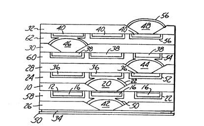
Figure 9 shows circuit board layer 10 including
an electrically insulating bonding film 24 placed between
adjacent layers. Additionally, Figure 9 shows circuit
board layers 26, 28, 30, and 32 which have been prepared
in accordance with the present invention, as set forth
30 above. Circuit board layers 26-32 include trace metal
layers 34, 36, 38, and 40, respectively. Via metal 42,
44, 46, and 48 is deposited in via holes of circuit board
layers 26, 28, 30, and 32, respectively. Cover metal
layers 50, 52, 54, and 56 are deposited on trace metal
35 layers 34, 36, 38, and 40 and via metal 42, 44, 46, and
48 of circuit boards 26, 28, 30, and 32, respectively.
As shown in Figure 9, the present invention is well
W094/29897 ~ ~g~ PCT~S94tO6387
-- 10 --
suited for forming blind and buried vias, as well as
stacked vias as shown by vias 44 46, and 42 and 20. The
electrically insulating bonding film layers 58, 24, 60,
and 62 are deposited on circuit board layers 26, 10, 28,
5 and 30 and separate adjacent circuit board layers. The
particular polymer used is a matter of choice although
epoxy compounds have been found to work well. While
Figure 9 shows only five layers, it will be understood
that the invention allows for lamination of a plurality
10 of circuit board layers to be assembled as shown to form
an interconnected structure. It should be noted as well
that such an interconnect could be used to attach a
single or multiplicity of layers to a rigid substrate.
For example, a flex circuit could be attached to a
15 printed circuit board by putting bumps on the flex and
pads on the board.
Following completion of the formation of
circuit board layers 10, 26, 28, 30, and 32, the circuit
board layers are stacked and aligned as shown in Figure
20 9. Specifically, the via metal bump layer of one layer
is aligned with its corresponding electrical pad on an
adjacent layer. The alignment can be performed by any
suitable means. Mechanical alignment using alignment
pins is one method that works well.
Once circuit board layers 10 and 26-32 are
aligned as shown in Figure 9, they are laminated together
under heat and pressure to form the structure shown in
Figure 10. The lamination causes an electrical contact
where the "bump" of the via metal of one layer contacts
30 an electrical pad of an adjacent layer and the low
melting point metal fuses together. Simultaneously, the
adhesive layers fuse together forming a mechanical bond
that holds the circuit board layers together and isolates
the electrical contacts. The lamination conditions are
35 a matter of choice and depend on the polymers and
metallurgies involved. Applicable pressure ranges
include 0.15 MPa - 5 MPa, more preferably 0.3 MPa - 3.5
W094l29897 216 2 ~ 9 ~ PCT~S94/06387
-- 11 --
MPa, and more preferably 0.7 - 1.7 MPa. Temperature
ranges for lamination are 80C-425C, more preferable
130-350C, and more preferably 175-280C. The metal-
metal bond is formed instantly and thus the lamination
5 time is dependant on the chosen adhesive bonding material
and the temperature at which the bonding takes place.
In another embodiment of the present invention,
circuit board layers are fabricated as described above.
The bumps and circuitry are then plated with at thin
10 conductive metallurgy for example gold, tin, nickel,
palladium and the like. In this embodiment of the
invention, the electrically insulating bonding material
58, 24, 60, and 62, used to bond the layers shown in
Figure 9 is an anisotropically conductive adhesive.
15 These adhesives are capable of conducting electricity in
one direction while insulating in the other two
directions. In this embodiment, there is no direct
metallic bonding of the metal pad and bump. Electrical
contact is made through a very thin layer of adhesive
20 pressed between a given bump and its corresponding pad.
An example of one type of anisotropically conductive
adhesive is described in U.S. Patent 5,143,785 issued
September 1, 1992 held by 3M. This adhesive is
structured such that when the adhesive is compressed
25 under heat and pressure to form a bond, small conductive
particles dispersed in the resin are trapped between the
bump and the contact pd and are compressed forming
electrical contacts between the bump and the contact pad.
The adhesive cures trapping the particles in place. No
30 metal reflow is needed for such a bond and thus
laminations can be performed at temperatures below the
melting point of the interface metallurgy.
Figure 11 shows a test sample 70 having circuit
board layers 72 and 74. Circuit board layer 72 carries
35 copper layer 76 and circuit board layer 74 carries copper
layer 78. "Bumps" 80, 82, 84, and 86 extend between
copper layer 76 and copper layer 78 and contact copper
W094/29897 PCT~S94/06387
~,~6~9~ --
- 12 -
layer 78 in accordance with the present invention. An
insulating dielectric adhesive layer 88 separates circuit
board 72 from circuit board 74.
Six samples similar to sample 70 were made.
5 Each sample had a total of 16 "bumps." Electrical
resistance measurements were made between copper layer 76
and copper layer 78. All six samples showed a resistance
of less than 0.10 Ohms. Circuit boards 72 and 74 were
pulled apart so that the individual "bumps" could be
10 examined. As the samples were pulled apart, most of the
bumps were transferred to copper layer 78 so that the
individual bumps could be tested. Using a four point
test probe, each bump had an electrical resistance of
less than 0.10 Ohms. Resistance measurements as low as
15 0.5 milli-Ohms have been observed.
When laminating circuit board layers of the
present invention, the edges may be sealed by allowing
the adhesive to overlap the edges. This improves the
reliability of the electrical interconnections under
20 conditions of high humidity and temperature. Samples
fabricated in the manner of these examples have survived
humidity aging tests for over 1000 hours at 85C and 85%
relative humidity.
In another example, many samples fabricated
25 from flexible Kapton polyimide substrate similar to that
of Figure 11 with 4 by 5 inch arrays of bumps with a
pitch of 40 mils and bump diameter and heights of less
than 200 and 25 ~m respectively and a tin cover
metallurgy were bonded to a tin plated copper substrate.
30 A high performance 9900 epoxy adhesive film available
from Minnesota Mining and Manufacturing Company of Saint
Paul, Minnesota was used as the bonding adhesive
Laminations were executed at 450F and 500 Psi for 30
minutes. Individual vias were isolated by etching the
35 surrounding copper after bonding and single via
resistances of less than 10 milli-Ohms were measured.
Examination of sectioned samples using optical and
W094/29897 ~1 6 2 4 9 9 PCT~S94/06387
.
- 13 -
scanning electron microscopy revealed reflow of the tin
at the bump-pad interface indicating good electrical
contact. Samples with a plurality of such layers have
been fabricated as well.
5The present invention provides an improved
electrical interconnection between adjacent circuit board
layers in a multi-layer circuit board. The fabrication
process for the circuit layers of the present invention
is based on the enhancement of the processing of fine
10 pitched metallized circuit layers which are already
produced in high volume for use in TAB and flex
circuitry. The lamination technology used to assemble
the circuit boards of the current invention is based on
the enhancement of conventional high volume printed
15 circuit board production. The invention includes a
simple improved method of electrical interconnection
which allows the combining of these two well developed
technologies to produce a circuit board that has
interconnect densities in the range of high density
20 circuits but is manufactured using conventional
techniques and materials at significantly lower cost.
Since all of the circuitry is fabricated prior to
lamination, each circuit layer can be inspected prior to
lamination into the full multi-layer structure thereby
25 increasing yield. Furthermore, fabricating the circuit
board in a single lamination step, so called parallel
processing, results in significant cost savings over the
prior art. The invention provides for a via formation
process that yields vias which are much smaller than the
30 prior PCB art and can be buried, blind and stacked
without additional processing. The smaller vias provide
for the resulting increase in circuit density achieved
using the current invention. The invention also provides
for a substrate with some inherent flexibility. The
35 present invention can be employed with a wide range of
dielectric films which are used to form individual
circuit board layers. Although a description of a "bump"
W094l29897 PCT~S94/06387
~ 4~ - 14 -
contacting an electrical pad has been shown, the present
invention can also be used where a "bump" contacts
another "bump."
Although the present invention has been r
5 described with reference to preferred embodiments,
workers skilled in the art will recognize that changes
may be made in form and detail without departing from the
spirit and scope of the invention. For example via holes
can be formed by any wet or dry process such as laser
lO ablation, reactive ion etching, mechanical punching,
photo imaging, chemical milling, mechanical forming,
casting etc. Different adhesives and dielectrics than
those described can be used. The adhesive layer can be
removed altogether replacing the dielectric substrate
15 film with a conformable film that bonds to the adjacent
layers. For example, conformable polyamide and the like.
The present invention can be used in forming multi-chip
modules, tape automated bonding of double metal (ground
plane) tape, and other microelectronic interconnect
20 devices.