Note: Descriptions are shown in the official language in which they were submitted.
CA 02162516 1998-08-18
-1-
AN ANALOG-TO-DIGITAL CONVERTER CIRCUIT
This invention relates to an analog-to-digital converter (hereinafter
abbreviated to "an AD converter") circuit, and more particularly to an AD
converter circuit whose dynamic range can be automatically controlled in
accordance with input signal levels.
In a case where an analog signal is converted to an equivalent
digital signal by an AD converter, if the level of the analog signal is so
small as
to be digitized within a considerably low quantization level in comparison
with
the maximum quantization level usable in the AD converter, the quality of the
converted digital signal is degraded by quantizing errors. In order to prevent
the
degradation, a circuit shown in Figure 7 has heretofore been used, wherein a
variable gain amplifier 51 and an analog level detector 52 are included.
The analog level detector 52 detects the level of an analog signal
55 which is input to an AD converter 53 from the output of the variable gain
amplifier 51. By negative feedback control of the variable gain amplifier 51
with
the output of the analog level detector 52, the amplitude of the analog signal
55
is maintained at a relatively constant level, regardless of level fluctuations
of an
input analog signal 54. Thus, when a reference voltage of the AD converter 53
is set to a value appropriate to the level of the analog signal 55, a high-
quality
digital signal 56 is obtained, with small quantizing errors.
However, there is a problem in the variable gain amplifier 51.
Usually, the variable gain amplifier 51 takes the form of a variable-
transconductance operational amplifier with a current control circuit.
Therefore,
the characteristic of the variable gain amplifier 51 varies considerably
because
of inequality of elements of the amplifier or because of temperature change.
So, sometimes the amplified analog signal 55 exceeds the maximum quantizing
range of the AD converter 53, or the amplified analog signal 55 remains so
small as to be quantized within a considerably-low quantization level in
comparison with the maximum quantization level of the AD converter 53.
CA 02162516 1998-08-18
-2-
When the analog signal 55 exceeds the maximum quantizing range
of the AD converter 53, the digital signal 56 will not be equivalent to the
input
analog signal 54, and when the analog signal 55 is so small as to be quantized
within a considerably low quantizing level in comparison with the maximum
quantizing level of the AD converter 53, the quantizing errors will become
large.
Furthermore, there is another problem in the AD converter circuit
of Figure 7. The AD converter circuit is used in a variety of applications.
For
example, there is a radio receiver in a communication system using QPSK
(quadrature-phase-shift keying) modulation system. The receiver demodulates
the QPSK modulated signals, and desired signal components among the
demodulated signals are digitized by AD converter circuits.
The receiver must exercise a well-balanced AGC (automatic gain
control) on the in-phase component (hereinafter abbreviated to I-component)
and on the quadrature-phase component (hereinafter abbreviated to Q-
component), and therefore the AGC is exercised in an intermediate-frequency
band (hereinafter abbreviated to IF band), and then an orthogonal
transformation is performed.
When broad-band signal components corresponding to desired
signals to be digitized are adjacent to narrow-band undesired signal
components, the undesired signal components can not effectively be attenuated
in the IF band. Therefore, the narrow-band undesired signal components must
be sufficiently attenuated by notch filters or low-pass filters after the
signals are
demodulated to a base band. Then the desired signal components of a broad
band are digitized.
Therefore, when the AD converter circuit of Figure 7 is used for
digitizing the desired signal components in a receiver as described for
receiving
the QPSK modulated signals, the circuit of Figure 7 must be modified, for
example, to a circuit shown in Figure 8.
An input analog signal 66 in the IF band is amplified by a variable
gain amplifier 61, and the amplitude level of the output IF signal 67 of the
variable gain amplifier 61 is detected by an analog level detector 62.
Negative
CA 02162516 1998-08-18
-3-
feedback control of the variable gain amplifier 61 with the output of the
analog
level detector 62 maintains an amplitude level of the output IF signal 67 at a
relatively constant level.
The output IF signal 67 is demodulated to a base band I-
component signal and a base band Q-component signal at a quadrature
demodulator 63. Undesired signal components superimposed on the base band
I-component signal and the base ban Q-component signal are attenuated by
filters 641 and 64Q respectively. After the undesired signal components are
attenuated, the output of the filter 641 and the output of the filter 64Q are
digitized at AD converters 651 and 65Q, respectively.
The output IF signal 67 includes the desired signal and the
undesired signal) and the output of the analog level detector 62 detects the
resultant amplitude of the desired signal and the undesired signal. Therefore,
if the undesired signal has a high level in the IF band, the gain of the
variable
gain amplifier 61 is unduly reduced for the desired signal. As a result,
quantizing errors become large and the quality of the digital signals obtained
is
degraded.
Another type of AD converter circuit has been proposed, wherein
a quantization reference voltage is controlled in proportion to the level of
the
output signal of the AD converter.
For example, there is a Japanese patent application entitled "An
AD converter circuit", laid open as Provisional Publication No. 371291'89.
Figure 9 shows a block diagram of the prior art. An analog signal
75 is converted to a digital signal 76 at an AD converter 71 with reference to
a
reference voltage 79 supplied from a DC shift circuit 74. The highest
quantization level of the AD converter 71 is adjusted, corresponding to the
reference voltage 79. Therefore, when the reference voltage 79 is large, a
unit
increment of the digital signal 76 represents a large voltage increment, and
when the reference voltage 79 is small, a unit increment of the digital signal
76
represents a small voltage increment.
CA 02162516 1998-08-18
-4-
The level of the digital signal 76 detected by a digital level detector
72, is converted to an analog signal 78 by a digital-to-analog converter
(hereinafter abbreviated to "DA converter") 73. A DC shift circuit 74 produces
the reference voltage 79 in proportion to the analog signal 78.
Thus, when the level of the analog signal 75 is low, the digital level
detector 72 detects a low level, the output of the DA converter 73 becomes
low,
reducing the reference voltage 79, and the low-level analog signal is
converted
to a digital signal having an incremental step of a small voltage difference,
preventing quantizing errors. And when the level of the analog signal 75 is
high, a high reference voltage 79 is supplied, preventing the high analog
signal
from going beyond the reference voltage.
The AD converter circuit shown in Figure 9 not only solves the
problems of the variable gain amplifier, but also eliminates the problem of
the
AD converter circuits of Figure 8. Specifically, when the AD converter circuit
of
Figure 9 is used as the AD converters 651 and 65Q of Figure 8, an insufficient
signal amplification at the variable gain amplifier 61 influenced by a
presence
of a strong undesired signal, will not produce quantizing errors, since a
small
reference voltage 79 is used in the AD converters 651 and 65Q for small input
signals.
The AD converter circuit of the prior art has a problem that the
circuit requires a DA converter, since the reference voltage 79 is produced
from
the digital signal 76 produced by the AD converter 71.
Another AD converter circuit wherein the reference voltage for
quantization is controlled also in accordance with an output level of the AD
converter, is disclosed in a Japanese patent application entitled "An
automatic
level control circuit of a sound recording and reproducing apparatus", laid
open
as Provisional Publication No. 313771'90 (hereafter called a "second prior
art").
In this second prior art, a DA converter is employed.
Therefore, a primary object of the present invention is to provide
an AD converter circuit having small quantizing errors, wherein a variable
reference voltage for quantization is generated with no DA converter.
CA 02162516 1998-08-18
-5-
In order to achieve the object, the reference voltage generator of
a first embodiment of this invention generates a quantization reference
voltage
from the level of an input analog signal.
Another object of this invention is to provide an AD converter
circuit wherein desired signal components are digitized to high precision in
the
presence of undesired signal components, when, for example, a demodulated
IF output signal containing undesired signal components is digitized.
In order to achieve this object, an AD converter of a second
embodiment of this invention digitizes the desired signal components,
extracted
through a filter from the demodulated IF output signal, referring to a
reference
voltage which decreases in proportion to the signal level of the undesired
signal
components extracted through another filter.
In the first embodiment, a reference voltage, which increases in
proportion to the input analog signal level, is obtained with no DA converter.
In the second embodiment, when undesired signal components are
strong, the desired signal components in the output of the IF demodulator will
be weak, because the undesired signal components and the desired signal
components, included in the IF band, are collectively gain-controlled by the
AGC. So, a reference voltage which decreases in proportion to the intensity of
the undesired signal components is obtained with no DA converter, and used
as the reference voltage referred to by the AD converter.
Further objects, features, and advantages of this invention will
become apparent from a consideration of the following description, the
appended claims, and the accompanying drawings in which the same numerals
indicate the same or corresponding parts.
Figure 1 is a block diagram of a first embodiment of the present
invention;
Figure 2 is a circuit diagram of the analog level detector of Figure
1;
Figure 3 is a circuit diagram of the proportional circuit of Figure 1;
CA 02162516 1998-08-18
-6-
Figure 4 is a block diagram of a second embodiment of this
invention;
Figure 5 is a circuit diagram of the inverse proportional circuit of
Figure 4;
Figure 6 is a modification of Figure 4;
Figure 7 shows a conventional AD converter circuit;
Figure 8 is a block diagram of an apparatus wherein output signals
of a quadrature demodulator are digitized by AD converter circuits of Figure
7;
Figure 9 is a block diagram of an AD converter circuit in a prior art.
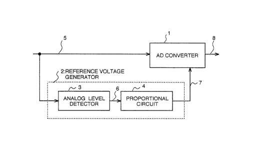
Referring to Figure 1, an input analog signal 5 at a signal input
terminal of an AD converter 1 is digitized into a digital output signal 8 with
reference to a reference voltage 7 supplied at a reference voltage input
terminal
of the AD converter 1. The input analog signal 5 is delivered to a signal
voltage
input terminal of a reference voltage generator 2 for generating the reference
voltage 7 supplied to the AD converter 1. An analog level detector 3 in the
reference voltage generator 2 detects an intensity level of the input analog
signal 5, and the detected analog signal 6 is converted to the reference
voltage
7 through a proportional circuit 4.
The AD converter 1 is, for example, a parallel-comparator-type AD
converter. The analog level detector 3 is a level detector for detecting an
intensity level, a peak level or an average level for example, of the input
analog
signal 5.
When the intensity level of the input analog signal 5 is low, a low
reference voltage 7 is supplied to the AD converter 1, and when the intensity
level of the input analog signal 5 is high, a high reference voltage 7 is
supplied
to the AD converter 1; thus the input analog signal 5 is converted to a
digital
signal 8, wherein quantizing errors are suppressed.
Figure 2 is a circuit diagram illustrating an example of the analog
level detector 3. The analog level detector 3 outputs a detected analog signal
6 charged in a capacitor C2 through a capacitor C1, a diode D2, and a resistor
R1 with the input analog signal 5. A diode D1 clamps the bottom voltage
CA 02162516 1998-08-18
_7_
through the capacitor C1 to the ground. The detected analog signal 6
represents an average intensity level of the input analog signal 5.
Figure 3 shows an example of the proportional circuit 4. The
detected analog signal 6 is connected to a positive input terminal of an
operational amplifier OP1 through a voltage divider circuit of R2 and R5. An
offset voltage Voff1 is connected to a negative input terminal of the OP1
through
a resistor R3, and a resistor R4 feeds back the output of the OP1 to the
negative input terminal of the OP1.
The value Vout of the reference voltage 7, which is the output of
the OP1, is represented by:
Vout = aVin1 - aVoff1 (1)
where Vin1 is the voltage of the detected analog signal 6. Positive
coefficients a and ,~ are determined by R2, R3, R4 and R5. The equation (1)
shows that the output voltage Vout increases in proportion to the input
voltage
Vin1.
Figure 4 is a block diagram of a second embodiment of the present
invention. In this embodiment, an input analog signal 41 in an IF band is
obtained by receiving a QPSK modulated signal. The input analog signal 41 is
amplified into an amplified analog signal 42 by a variable gain amplifier 31.
The
variable gain amplifier 31 is automatic-gain-controlled, with the output of an
analog level detector 32 and the amplitude of the amplified analog signal 42
being maintained at a relatively constant level.
The amplified analog signal 42 in the IF band is demodulated by
a quadrature demodulator 33 to a base-band I-component signal and a base-
band Q-component signal. When there are undesired signal components whose
frequency band is adjacent to the frequency band of the desired signal
components, the variable gain amplifier is gain-controlled with components
both
of desired signal and undesired signal, and undesired components may appear
both at the base-band I-component signal and the base-band Q-component
signal.
CA 02162516 1998-08-18
- 8 _
At the base band, the undesired signal components can be
separated from the desired signals. Desired signal components in the base-
band I-component signal are extracted by a desired-signal extracting filter
341
and are delivered to an AD converter 351, while desired signal components in
the base-band Q-component signal are extracted by another desired-signal
extracting filter 34Q and are delivered to another AD converter 35Q.
Undesired signal components in the base-band I-component signal
are extracted by an undesired-signal extracting filter 361 and are delivered
to a
reference voltage generator 391, and undesired signal components in the base
band Q-component signal are extracted by another undesired-signal extracting
filter 36Q and are delivered to another reference voltage generator 39Q.
Each of the reference voltage generators 391 and 39Q comprises
an analog level detector 3 and an inverse proportional circuit 9. The analog
level detector 3 has been explained in connection with Figure 2.
Figure 5 shows an example of a circuit diagram of the inverse
proportional circuit 9. A detected analog signal, for example, 431 of the
output
of the analog level detector 3 in the reference voltage generator 391, is
connected to the negative input terminal of an operational amplifier OP2
through
a resistor R7. An offset voltage Voff2 is connected to the positive input
terminal
of the OP2 through a voltage divider composed of R6 and R9. The output of
the OP2 is fed back through R8 to the negative input terminal of the OP2. The
output voltage Vout of the OP2 is represented by:
Vout = ~yVoff2 - 6Vin2 (2)
where Vin2 is the voltage of 431. As the coefficients ~y and b are
both positive, Vout decreases in proportion to Vin2.
The output voltage 441 from the reference voltage generator 391
is supplied to the AD converter 351 as the reference voltage, and the output
voltage 44Q from the reference voltage generator 39Q is supplied to the AD
converter 35Q as the reference voltage.
When the input analog signal 41 in the IF band includes a large
amount of undesired signal components, the intensity of the desired signal
CA 02162516 1998-08-18
_g_
components in the amplified signal 42 in the IF band decrease in proportion to
the intensity of the undesired signal components, because the gain of the
variable gain amplifier 31 is controlled to output the amplified signal 42,
which
is composed of desired signal components and the undesired signal
components, at a constant intensity level.
In the embodiment, the output analog signals from the desired
signal extracting filters 341 and 34Q are quantized with reference to the
reference voltages 441 and 44Q, which decrease in proportion to the intensity
of the undesired signal.
Thus, when the intensity level of the undesired signal components
is high, low level desired signal components are quantized by low-level
reference voltages 441 and 44Q, and the output digital signals 451 and 45Q are
high-quality signals including few quantizing errors.
Each of the output signals of the desired-signal extracting circuits
341 and 34Q might be digitized by the AD converter circuit of Figure 1, as
shown
in Figure 6, but the AD converter circuit of Figure 4 is preferred. The reason
is
that the reference voltage generator 2 has an interfering effect on the output
signals of the desired signal extracting filters 341 and 35Q, and may cause
errors on the inputs to the AD converters 351 and 35Q.