Note: Descriptions are shown in the official language in which they were submitted.
- 21 62534
~H 236 CA
Arrangement for the Linearization and Temperature
Compensation of Sensor Signals
FIELD OF THE lNV~N'l'ION
The present invention deals with the linearization and
temperature compensation of signals from capacitive
sensors, since the capacitance of such sensors commonly
exhibits a nonlinear dependence on the measurand, such
as a pressure, and on temperature.
BACRGROUND OF THE lNV~N'l'lON
Capacitive sensors are used, for example, as capacitive
.pressure sensors to measure pressure or as capacitive
humidity or moisture sensors to measure humidity or
( ) moisture but can also be employed-to measure the
pressure changes caused by a-Rarman-vortex street in
vortex flowmeters.
U.S.- Patent 5,257,210 describes comprehensively how
erroneous components of the measurand can be linearized
and compensated for. The principle of this
linearization and compensation consists of first.
deriving from the measurand an electric signal, herein-
after referred to as "sensor signal", and only then
impressing on the sensor signal a disturbance signal
generated by a further sensor per disturbance variable.
- 21 62534
-- 2 --
In the embodiments of U.S. Patent 5,257,210 relating to
capacitive pressure sensors with a measuring capacitor
and a reference capacitor, therefore, the disturbance
signals are processed, together with the sensor
signals, only in stages following the measuring and
reference capacitors by switched-capacitor quantized
charge transport. To accomplish this, several
functional units are provided which are controlled by
clock signals having a period equal to forty times that
of a basic clock signal. The circuitry of the
functional units is rather-complicated, so that the
total number of components required for them is
considerable. Also, those forty basic clock signal
periods must have elapsed before the prior art
arrangement has generated the compensated and desired
smoothed output signal.
SUMMARY OF THE lNv~NlION
- It is, therefore, an object of the invention to provide
and arrangement which requires substantially fewer
components than the prior art arrangement and wherein
-- the compensated smoothed output signal is obtained
faster than in the prior art arrangement.
To attain this object, the invention consists in the
provision of an arrangement for the linearization and
temperature compensation of sensor signals from
capacitive sensors which comprises:
- a measuring capacitor;
- a temperature-dependent voltage divider with a
resistive temperature sensor connected between an
operating potential and a first reference potential,
particularly ground, and measuring the temperature
of the measuring capacitor;
2 1 62534
- a clocked adjusting circuit for the output signal of
the arrangement which acts on the measuring capacitor
and a reference capacitor by means of analog signals,
-- with a first input of the adjusting circuit
connected to the operating potential, and a second
input to the temperature sensor;
- an integrating stage connectable under clock control-
to the measuring capacitor and the reference
capacitor
-- whose output is connected to a third input of the
adjusting circuit and is the output of the
arrangement; and
- a clock generator,
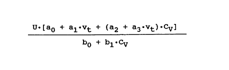
-- with the output signal, S, obeying the following
equation:
U- taO + al-Vt + (a2 + a3 Vt) Cv]
bo + bl CV
--- where
Cv is one of the following capacitance ratios:
Cvl = ( Cm Cr ) /Cm
CV2 = ( Cm ~ Cr) / ( Cm + Cr)
CV3 = ( Cm ~ Cr) /Cr;
Cm is the capacitance of the measuring capacitor;
C, is the capacitance of the reference capacitor;
U is the operating potential;
aO is a zero adjustment value;
a1 is a temperature coefficient zero adjustment
value;
a2 is a first span adjustment value;
a3 is a temperature coefficient span adjustment
value;
bo is a second span adjustment value;
21 62534
-- 4 --
bl is a linearization adjustment value, and
v, is the temperature-dependent resistance ratio
of the voltage divider.
In a preferred embodiment of the invention, the
integrating stage contains a first integrator and a
. second integrator, the first integrator comprising a
capacitor whose polarity must be reversed under clock
control, and the second integrator being connectable
under clock control to the output of the first
10 . integrator.
In another preferred embodiment of the invention, the
adjusting circuit comprises:
- a first digital-to-analog converter providing a
positive converter signal and a negative converter
signal,
-- whose reference input is the first input of the
adjusting circuit,
-- whose first signal input is supplied with the
~ digitized zero adjustment value,.A~,
2.u -- whose second signal input is supplied with the
digitized first span adjustment value, A2, and
- -- whose first and second signal enable inputs are
controlled by the clock generator;
- a second digital-to-analog converter providing a
positive converter signal and a negative converter
signal,
-- whose reference input is the second input of the
adjusting circuit,
-- whose first signal input is supplied with the
digitized temperature coefficient zero adjustment
value, Al,
- 2 1 62534
-- whose second signal input is supplied with the
digitized temperature coefficient span adjustment
value, A3, and
-- whose first and second signal enable inputs are
controlled by the clock generator;
- a third digital-to-analog converter providing a
positive converter signal and a negative converter
- signal,
-- whose reference input is the third input of the
adjusting circuit,
-- whose first signal input is supplied with the
digitized second span adjustment value, Bo~
-- whose second signal input is supplied with the
digitized linearization adjustment value, Bl, and
-- whose first and second signal enable inputs are
controlled by the clock generator;
- a first summer and a second summer each having one
output and six inputs,
-- the first and second inputs of the first summer
receiving, respectively, the positive and negative
-~ converter signals of the third digital-to-analog
converter via a first switch and a second switch,
-- the first and second inputs of the second summer
receiving, respectively, the positive and negative
converter signals of the third digital-to-analog
converter via a third switch and a fourth switch,
-- the third and fourth inputs of the first summer
receiving, respectively, the positive and negative
converter signals of the first digital-to-analog
converter via a fifth switch and a sixth switch,
-- the third and fourth inputs of the second summer
receiving, respectively, the positive and negative
2 1 62534
converter signals of the first digital-to-analog
converter via a seventh switch and an eighth switch,
-- the fifth and sixth inputs of the first summer
receiving, respectively, the positive and negative
converter signals of the second digital-to-analog
converter via a ninth switch and a tenth switch, and
-- the fifth and sixth inputs of the second summer
receiving, respectively, the positive and negative.
converter signals of the second digital-to-analog
converter via an eleventh switch and a twelfth
switch, with
--- the output of the first summer and the output
of the second summer connected via a 13th switch
and a 14th switch, respectively, to the measuring
capacitor,
--- the output of the first summer and the output of
the second summer connected via a 15th switch and
a 16th switch, respectively, to the
reference capacitor, and
--- the respective terminals of the measuring capacitor
and reference capacitor remote from the switches
connected to the first reference potential.
In a further preferred embodiment of the invention, for
the capacitance ratio Cvl = (Cp - Cr)/Cp or the
capacitance ratio Cv2 = (Cp - Cr)/(Cp + Cr), the first
integrator comprises:
- a first operational amplifier,
-- whose inverting input is connected via a 17th switch
to the measuring capacitor and via an 18th switch to
the reference capacitor,
--- with the junction of the 18th switch and the
reference capacitor connected via a l9th switch to
a second reference potential,
- 21 62534
-- 7 --
-- whose noninverting input is also connected to the
second reference potential,
-- whose inverting input is connected to the output via
three parallel branches,
--- the first of which consists of a 20th switch and a
21st switch in series,
--- the second of which consists of a 22nd switch and
a 23rd switch in series, and
--- the third of which consists of a 24th switch,
---- with the capacitor connected between the junction
of the 20th and 21st switches and the junction of
the 22nd and 23rd switches.
In another preferred embodiment of the invention, the
second integrator comprises:
- a second operational amplifier
-- whose inverting input is connected via a 25th switch
to the junction of the 20th and 21st switches and
via a fixed capacitor to the output of the
arrangement, and
-- whose noninverting input is connected to the second
reference potential.
- If the capacitance-ratio Cv3 = (Cm - C,)/C, is used, a
26th switch must be connected between the reference
potential and the junction of the 17th switch and the
measuring capacitor.
In a further preferred embodiment of the invention, the -
output of the integrating stage is coupled to a
smoothing stage.
21 62534
-- 8
In still another preferred embodiment of the invention,
to control the 26 switches and the respective signal
enable inputs of the three digital-to-analog
converters, the clock generator generates, from a basic
clock signal, clock signals having a positive level and
a more negative level, the r~spective level occurring
during at least one eighth of the period of the basic
clock signal.
BRIEF DESCRIPTION OF THE DRAWINGS
Further features and advantages of the invention will
become apparent from the following description of
embodiments illustrated in the accompanying drawings,
in which:
Fig. 1 is a schematic circuit diagram of a first
embodiment of the invention;
Fig. 2 is a schematic circuit diagram of a second
embodiment of the invention;
Fig. 3 shows the schematic circuit diagram of
Fig. 1 with further advantageous features;
Fig. 4 shows the schematic circuit diagram of
of Fig. 2 with the further advantageous
features of Fig. 3;
Fig. 5 shows the waveforms of clock signals if
the capacitance ratio (Cm - Cr)/Cm is to be
compensated with an arrangement as illus-
trated in Fig. 3 or Fig. 4;
- 2 1 62534
Fig. 6 shows the waveforms of clock signals if the
capacitance ratio (Cm - Cr)/(Cm + Cr) is to be
compensated with an arrangement as illustrated
in Fig. 3 or Fig. 4;
S Fig. 7 shows the waveforms of clock signals if the
capacitance ratio (Cm - Cr)/Cr is to be
compensated with an arrangement as illustrated
in Fig. 3 or Fig. 4;
Fig. 8 is a schematic circuit diagram of a specific
current-copier circuit usable in the arrange-
ment of the invention;
Fig. 9 shows a current-to-voltage converter usable in
connection with the circuit of Fig. 8;
Fig. 10 shows the switch positions in the arrangement
of Fig. 3 during period Dl of Fig. S;
Fig. 11 shows the switch positions in the arrangement
of Fig. 3 during period D2 f Fig. S;
Fig. 12 shows the switch positions in the arrangement
of Fig. 3 during period D3 of Fig. 5;
Fig.-13 shows the switch positions in the arrangement
of Fig. 3 during period D4 of Fig. S;
Fig. 14 shows the switch positions in the arrangement
of Fig. 3 during period D5 of Fig. S;
- 2 1 62534
-- 10 --
Fig. 15 shows the switch positions in the arrangement
of Fig. 3 during period D6 of Fig. 5;
Fig. 16 shows the switch positions in the arrangement
of Fig. 3 during period D, of Fig. 5;
Fig. 17 shows the switch positions in the arrangement
of Fig. 3 during period D8 Of Fig. S; and
Fig. 18 shows the switch positions in the arrangement
of Fig. 3 during period D9 of Fig. S;
DETAILED DESCRIPTION OF THE lNV~Nl'ION
The schematic circuit diagram of Fig. 1 contains a
measuring capacitor Km of capacitance Cm`and a reference
capacitor Kr of capacitance Cr. In the case of a pressure
sensor, the measuring capacitor K~ is pressure-dependent
and the reference capacitor Kr is as pressure-
'~ independent as possible, with both capacitors
preferably implemented within the pressure sensor. The
construction of such capacitive pressure sensors is
apparent, for example, from Fig. 2 of the above-
mentioned U.S. Patent 5,257,210 or from U.S. Patent
S,005,421.
In the case of humidity or moisture sensors with a
humidity- or moisture-sensitive measuring capacitor K
the reference capacitor Kr can be implemented, for
example, by making a conventional humidity or moisture
sensor humidity- or moisture-insensitive by means of a
humidity- or moisture-proof cover layer. In the
- 2 1 62534
-- 11 --
various cases it is thus advantageous if the reference
capacitor Rr is as insensitive to the measurand as
possible and can therefore be regarded as constant.
To obtain the compensated analog output signal S, the
invention uses one of the three capacitance ratios
CV1 = ( Cm Cr ) /Cm
Cv2 (Cm Cr)/(Cm + Cr)
Cv3 = ( Cm Cr ) /Cr
To generate a signal which is, as exclusively as
possible, a measure of the temperature of the sensor,
i.e., to generate a temperature-dependent signal, use
is made of a voltage divider 71 which is connected
between a first reference potential SN of the
arrangement and an operating potential U and consists
of a resistive temperature sensor ~ of resistance Re
and a dropping resistor 72 of resistance R~. The
temperature-dependent resistance ratio of this voltage
divider will be designated v,. Thus, v, = Re/(Re+R~). The
tap of the voltage divider 71 thus provides a signal
s = U v, = U-Re/(Re+R~).
-The voltage divider 71 is the simplest implementation
of a temperature sensor, but the scope of the invention
is not limited thereto. If required, any suitable
temperature-dependent network can be used. For
instance, a temperature-independent resistor could be
connected in parallel with the resisitive temperature
sensor, or a temperature-dependent bridge circuit could
be provided.
-- 21 62534
- 12 -
The first reference potential SN is preferably the
potential of the voltage reference point in the
arrangement. If that is notthe case, the first
reference potential SN may be approximately one half of
the value of the operating potential U, for example.
Unlike in the arrangements described in the above-
mentioned U.S. Patent S,257,210, in the invention, an
adjusting circuit 30 is provided which acts directly on
the measuring capacitor K~ and the reference capacitor
K, to effect linearization and temperature compensation.
The analog signals provided by the adjusting circuit 30
are applied directly to the measuring and reference
capacitors K~, K, under clock control. Thus, correction
signals are fed to the measuring and reference
capacitors Rm~ K, so that the output signal S of the
arrangement has the desired linear and temperature-
compensated waveform.
This direct action on the sensor signal makes it
possible in a simple manner to apply, in addition to
6~ the signals effecting linearization and temperature
compensation, span adjustment signals, zero adjustment
signals, etc., as ~ill be explained below.
The adjusting circuit 30 is controlled by clock signals
provided by a clock generator 61, see below. -A first
input of the adjusting circuit 30 is connected to the
operating potential U, and a second input is connected
to the tap of the temperature-dependent voltage divider
71, i.e., to the junction of temperature sensor ~ and
resistor 72.
21 62534
- 13 -
Connected under clock control to the measuring
capacitor Km and the reference capacitor Kr is an
integrating stage 50, whose output is the output of the
arrangement and provides the output signal S. This
output is coupled to a third input of the adjusting
circuit 30.
If necessary, the output signal S can be smoothed with
a smoothing stage 55, in the simplest case a smoothing
capacitor of sufficient capacitance, which must be
connected to the output of the integrating stage 50, as
can be seen in Fig. 3.
In the invention, the output signal S obeys the
following equation:
U [ aO + al v, + ( a2 + a3 - V, ) Cv ]
S =
bo + bl Cv
where Cv is one of the following capacitance ratios:
CV1 = ( Cm Cr ) /Cm
CVZ ( Cm Cr ) / ( Cm + Cr )
CV3 = (Cm Cr)/Cr;
Cm is the capacitance of the measuring
capacitr Rm;
Cr is the capacitance of the reference
capacitr Kr;
U is the operating potential;
aO is a zero adjustment value; -
al is a temperature coefficient zero
adjustment value;
a~ is a first span adjustment value;
2 1 62534
- 14 -
a3 is a temperature coefficient span
adjustment value;
bo is a second span adjustment value;
bl is a linearization adjustment value, and
v, is the temperature-dependent resistance
ratio of the voltage divider 71.
The adjusting circuit 30 comprises first, second, and
third digital-to-analog converters 31, 32, and 33,
respectively, each of which provides a positive
converter signal and a negative converter signal. The
two converter signals are equal in magnitude relative
to the first reference potential SN. The respective
negative converter signal can be derived, for example,
from the associated positive converter signal by means
of an analog multiplier that multiplies by a factor
of -1.
The respective digital-signal inputs of the three
digital-to-analog converters 31, 32, 33 are supplied
with digital signals Ao~ Al A2, A3, Bo~ B1, which are
formed from the above-mentioned adjustment values aO,
a1, a2, a3, bo~ b1, for example, and may come, for
example, from an electronic memory, such as an EEPROM,
- in which they were stored. It is also possible,
however, to form digital signals with the digital
values corresponding to the analog adjustment values aO,
al, a2, a3, bo~ bl directly and apply them directly to the
digital-to-analog converters, e.g. via a suitable data
bus.
2 1 62534
- 15 -
Each of the three digital-to-analog converters 31, 32,
33 has a reference input. These reference inputs are
supplied with different analog-signals which represent
the respective values to which the digital-to-analog
conversions are referred. Associated with each digital-
signal input is a signal enable input, so that each
digital-to-analog converter has two signal enable
inputs, each of which is supplied with one of the clock
signals T27, T28 from the clock generator 61-.
The reference input of the first digital-to-analog
converter 31 is the first input of the adjusting
circuit 30. It is connected to the operating potential
U, as was mentioned above. The first signal input of
the first digital-to-analog converter 31 is fed with
the digitized zero adjustment value Ao~ and the second
signal input with the digitized first span adjustment
value A2-
The reference input of the second digital-to-analog
converter 32 is the second input of the adjusting
2~ circuit 30. This input is connected to the tap of the
temperature-dependent voltage divider 71 and, thus, to
the temperature-dependent signal U v" as was mentioned
above. The first signal input of the second digital-to-
analog converter 32 is fed with the digitized
-temperature coefficient zero adjustment value Al, and
the second signal input with the digitized temperature
coefficient span adjustment value A3.
The reference input of the third digital-to-analog
converter 33 is the third input of the adjustment
- 2 1 62534
- 16 -
circuit 30. It is supplied with the output signal S, as
was mentioned above. The first signal input of the
third digital-to-analog converter 33 is fed with the
digitized second span adjustment value Bo~ and the
second signal input with the digitized linearization
adjustment value B1.
The adjusting circuit 30 further includes a first
summer 41 and a second summer 42 each having six inputs
and one output.
The first and second inputs of the first summer 41 are
suppliedj respectively, with the positive and negative
converter signals of the third digital-to-analog
converter 33 via first and second switches 1, 2.
The first and second inputs of the second summer 42 are
supplied, respectively, with the positive and negative
converter signals of the third digital-to-analog
converter 33 via third and fourth switches 3, 4.
- The third and fourth inputs of the first summer 41 are supplied, respectively, with the positive and negative
converter signals of the first digital-to-analog
converter 31 via fifth and sixth switches 5, 6.
The third and fourth inputs of the second summer 42 are
supplied, respectively, with the positive and negative
converter signals of the first digital-to-analog
converter 31 via seventh and eighth switches 7, 8.
The fifth and sixth inputs of the first summer 41 are
supplied, respectively, with the positive and negative
2 1 62534
- 17 -
converter signals of the second digital-to-analog
converter 32 via ninth and tenth switches 9, 10.
The fifth and sixth inputs of the second summer 42 are
supplied, respectively, with the positive and negative
converter signals of the second digital-to-analog
converter 32 via eleventh and twelfth switches 11, 12.
The respective terminals of the measuring and reference
capacitors Km~ Kr remote from the switches are connected
to the first reference potential SN. Since the voltage
divider 71 and the operating potential U are also
referred to the first reference potential SN, only
ratios are processed in the arrangement.
The outputs of the first and second summers 41, 42 are
connected, via a 13th switch 13 and a 14th switch 14,
respectively, to the measuring capacitor Km and, via a
15th switch 15 and a 16th switch 16, respectively, to
the reference capacitor Kr.
`~ Fig. 2 shows a second embodiment in a schematic circuit
diagram. It differs from the embodiment of Fig. l in
that instead of the three digital-to-analog converters
31, 32, 33, tapped resistors RaO~ R,l~ R~2, ~30~ Rbo~ Rbl are
provided, by means of which the analog adjustment
quantities aO, a1, a2, a3, bol bl are generated.
The broken vertical line at the left in Fig. 2
indicates the interface with regard to the
implementation of the arrangement: The tapped resistors
can be implemented using hybrid technology, for
- 21 62534
- 18 -
example, and the portion of the arrangement located on
the right of this line can advantageously be realized
- using semiconductor monolithic integrated circuitry.
If the user of the arrangement is to be permitted to
change the adjustment quantities at least in part, the
tapped resistors will be implemented as potentiometers,
for example. If the arrangement is preset by the
manufacturer, the tapped resistors will be implemented
as, preferably laser-trimmed, semiconductor or thin-
film resistors.
Each tapped resistor Ro~ R,2 is connected as a voltage
divider between the first reference potential SN and
the operating potential U. The taps of the resistors Ro
and R,2 are connected via further switches 271 and 281,
respectively, to the input of an analog inverter-Il and
to the fifth switch 5 and the seventh switch 7. The
output of the analog inverter I1 is coupled to the sixth
switch 6 and the eighth switch 8. The switch-271 is
~- supplied with the clock signal T27, and the switch 28
with the clock signal T28-
The taps of the resistors R~l and R~ are connected via
further switches 272 and 282, respectively, to the
ungrounded terminal of the temperature sensor ~, to the
input of an analog inverter I2, and to the ninth switch
9 and the eleventh switch 11. The output of the analog
inverter I2 is coupled to the tenth switch lO and the
twelfth switch 12. The switch 272 is supplied with the
clock signal T27, and the switch 282 with the clock
signal T28. Thus, in Fig. 2, two voltage dividers
-- 2 1 62534
-- 19 --
corresponding to the voltage divider 71 of Fig. 1 and
each ContAi n; ng the temperature sensor ~ are
implemented when the associated switches 272 and 282,
respectively, are closed.
Each tapped resistor Rbo, Rb1 is connected as a voltage
divider between the first reference potential SN and
the output of the arrangement; these resistors are thus
supplied with the smoothed output signal S. The taps of
the resistors Rbo and Rb1 are connected via further
switches 273 and 283, respectively, to the input of an
analog inverter I3 and to the first switch 1 and the
third switch 3. The output of the analog inverter I3 is
coupled to the second switch 2 and the fourth switch 4.
The switch 273 is suppIied with the clock signal T27, and
the switch 283 with the clock signal T28.
In Figs. 3 and 4, which show preferred embodiments of
the arrangements of Figs. 1 and 2, respectively, only
the parts of the circuit located at the right differ
- from those of Figs. 1 and 2, so that only these right-
hand parts will be explained; they are preferred
embodiments of the integrating stages 50 of Figs. 1 and
2.
The signals present at the measuring and reference
capacitors Rm~ Rr are applied under clock control to a
- first integrator 51. The latter includes a first
operational amplifier 53, whose inverting input is
connected via a 17th switch 17 to the measuring
capacitor Rm and via an 18th switch 18 to the reference
capacitor Rr~ with the junction of the 18th switch and
2 1 62534
- 20 -
the reference capacitor connected via a l9th switch 19
to a second reference potential Ur.
This second reference potential U, is different from
ground potential and from the operating potential U. It
preferably lies approximately in the middle between the
first reference potential SN and the operating
potential U, for example. Thus, if a value of, for
example, +5V is fixed for the operating potential U,
the second reference potential Ur will be chosen to be
around +2.5V.
Also connected to the second reference potential U, is
the noninverting input of the first operational
amplifier 53, whose inverting input is connected to the
output via three parallel branches. The first parallel
branch consists of a 20th switch 20 and a 21st switch
21 in series; the second parallel branch consists of a
22nd switch 22 and a 23rd switch 23 in series, and the
third parallel branch consists of a 24th switch 24. A
i- capacitor ~, whose polarity must be reversed,is
connected between the junction of the 22nd and 23rd
switches and the junction of the 20th and 21st
switches; the latter junction is also the output of the
first integrator 51.
The signal appearing at the output of the first
integrator 51 is applied under clock control to a
second integrator 52. The latter comprises a second
operational amplifier 54, whose inverting input is
connected via a 25th switch 25 to the junction of the
20th and 21st switches and via a fixed capacitor ~ to
the output of the arrangement, and whose noninverting
input is connected to the second reference potential U,.
- 21 62534
- 21 -
In the arrangement explained so far, the signal
processing is based either on the capacitance ratio
Cvl = (Cm - Cr)/Cm or on the capacitance ratio
Cv2 = (Cm - Cr)/Cm + Cr). If the capacitance ratio
CV3 = (Cm - Cr)/Cr is to be processed, a 26th switch 26
must be placed between the second reference potential Ur
and the junction of the 17th switch 17 and the
measuring capacitor Km.
The clock generator 61 generates, from a basic clock
signal, 28 clock signals Tl ... T28 for controlling the
26 switches 1 ... 26-and the respective signal enable
inputs of the three digital-to-analog converters 31,
32, 33, see Figs. 5 to 7. The clock signals T1 ... T28
have a positive level H or a more negative level L. The
respective level occurs during at least one eighth
D~ ... D8 f the period D = ~(D1 ... D8) of the basic
clock signal.
The respective H levels switch the 26 switches and the -
respective switches of the six signal enable inputs of
-~ the three digital-to-analog converters 31, 32, 33 into
the conducting state, and the respective L levels
switch these switches into the nonconducting state. The
switches are preferably implemented-with electronic
components, such as transistors, particularly
insulated-gate field-effect transistors.
The clock signals Tl ... T28 are derived in the clock
generator 61 from an oscillator signal having a period
equal to D1, e.g., by frequency division and logical
combination of the frequency-divided signals, as is
- 2 1 62534
- 22 -
familiar to those skilled in the art. The above-
mentioned basic clock signal is obtained by dividing
the frequency of the oscillator signal by 8.
The clock signals Tl3, Tl7 of Fig. 5, for example, are
generated by dividing the oscillator signal by 2 and
are 180 out of phase with respect to each other. The
clock signals T4, T7, Tl1 of Fig. 5 are derived from the
basic clock signal, and their H levels have been placed
in the fifth eighth Ds of the period D.
The assignment of the respective H and L levels to the
individual eighths of the period of each clock signal
- and their effect will now be described in more detail.
Fig. 5 shows the waveforms of the clock signals T
during one period D of the basic clock signal for the
capacitance ratio Cvl = (Cm - Cr)/Cm. As can be seen, a
few of the clock signals are at a constant L level,
namely the clock signals Tl4, T~, so that actually the
- switches 14, 26 controlled by them need not be
implemented and the clock signals Tl4, T~ need not be
generated.
Fig. 6 shows the waveforms of the clock signals T
during one period D of the basic clock signal for the
capacitance ratio Cvl = (Cm - Cr)/(Cm + Cr). Here, too, a
few of the clock signals are at a constant L level,
namely the clock signals Tl4, Tls, Tl9, T~, so that
actually the switches 14, 15, 19, 26 controlled by them
need not be implemented and the clock signals T14, T1s,
Tv, T~ need not be generated.
21 62534
- 23 -
Fig. 7 shows the waveforms of the clock signals T
during one period D of the basic clock signal for the
capacitance ratio Cvl = (Cm - Cr)/C,. Here, too, a few of
the clock signals are at a constant L level, namely the
clock signals Tl5, Tlg, so that actually the switches 15,
19 controlled by them need not be implemented and the
clock signals Tl5, Tlg need not be generated.
The reason why these switches and clock signals, which
are not needed to implement the respective capacitance
ratios, are shown nevertheless is that in Figs. 1 to 4,
the common circuit for implementing any of the three
variations Cvl, Cv2, Cv3 of the capacitance ratio of the
arrangement is illustrated. Because of these
systematics of the representation of the invention,
however, the switches not needed for a particular
capacitance ratio and the corresponding clock signals
are included in Figs. 1 to 4 and Figs. 5 to 7,
respectively.
If the measurement is to be based on only one of the
~o three capacitance ratios, those switches to which a
constant L level is applied need not be implemented and
the associated clock signals need not be generated, of
course.
As can be seen from the waveforms of the clock signals
of Figs. 5 to 7, during the second four periods
D5 ... D8, the respective inverse outputs, compared to
the periods Dl ... D4, of the digital-to-analog
converters 31, 32, 33 of Figs. 1 and 3 and the inverse
signals of the tapped resistors of Figs. 2 and 4 are
2 1 62534
- 24 -
applied through the respective switches to the
capacitors Km ~ Kr -
Furthermore, in the embodiments of Figs. 3 and 4, the
polarity of the capacitor Ku is reversed during the
second four periods D5 ... D8 from that during the first
four periods D1 ... D4 by means of the associated
switches. This periodic polarity reversal makes it
possible to compensate offset voltages of the
operational amplifiers in the arrangement, and may be
referred to as "chopper technique".
Fig. 8 shows the schematic circuit diagram of a
specific current-mirror circuit, referred to here as
"current copier" to distinguish it from conventional
current mirrors. This current copier 80 will be used to
advantage if in the embodiments of Figs. 2 and 4, i.e.,
in the embodiments with resistors as generators of the
analog adjustment quantities aO, a1, a2, a3, bo~ b1, the
inputs of the summers 41, 42 are to be supplied with
voltage signals which are as ideal as possible, i.e.,
with voltages from a voltage source having as low an
internal resistance as possible. With the respective
taps at the voltage dividers, drawn as direct taps in
Figs. 2 and 4 to simplify the illustration, this
condition is not fulfilled, of course.
A current copier as shown in Fig. 8 generates a current
which is independent of the potential at the respective
voltage-divider tap. The current is then transformed,
by means of a current-to-voltage converter as shown in
Fig. 9, into a voltage which is delivered by a voltage
source with a low internal resistance.
2 1 62534
Referring to Fig. 8 in more detail, there is shown a
first series combination 81 of two transistors 83, 84
of complementary conductivity type which have their
controlled current paths connected in series between
the operating potential U and the first reference
potential SN.
The figure further shows a second series combination 82
; of two transistors 85, 86 of complementary conductivity
type which have their controlled current paths
connected in series between the operating potentiaI U
and the first reference potential SN.
The control terminals of the two transistors 83, 85 of
one conductivity type are connected together, and so
are the control terminals of the two transistors 84, 86
of the other conductivity type.
The circuit symbol shown for the transistors of each
series combination 81, 82 in Fig. 8 is that of
enhancement-mode insulated-gate field-effect
transistors - transistors 83 and 85 are p-channel
transistors, and transistors 84 and 86 n-channel
transistors -, but other types of transistors are also
usable; this depends on the specific implementation
technology used.
The junction of the current paths of the transistors
83, 84 of the first series combination 81 is coupled to
the inverting input of a further operational amplifier
87, whose noninverting input is connected to the second
reference potential U,. The operational amplifier 87 has
a differential output whose positive terminal is
`- 21 62534
- 26 -
connected to the junction of the control terminals of
the two transistors 84, 86, and whose negative terminal
is connected to the junction of the control terminals
of the two transistors 83, 85. These terminals are also
connected via capacitors 88.and 89, respectively, to
the junction of the controlled current paths of the
transistors of the first series combination 81.
Also indicated in Fig. 8 is the behavior of the current
copier with respect to the input current I. The input
current I divides into a "positive" current Ip, which
flows through the transistor 83, and a "negative"
current IN~ which flows through the transistor 84.
Corresponding - copied - currents I'p and I 'N flow
through the transistors 85 and 86, respectively, of the
second series combination 82 and add to form the -
copied - current I'.
The current-to-voltage converter 90 shown in Fig. 9
serves to convert the current I' of Fig. 8 into an
-:~ output voltage U,. To this end, the output of the
current copier 80 must be coupled to the input of the
current-to-voltage converter 90. The latter consists of
a further operational amplifier 91, which has its
inverting input connected via a resistor 92 of
resistance R~ to its output, and which is the input.of
the current-to-voltage converter 90, while the
noninverting input is connected to the second reference .
potential Ur. Thus the output voltage is: U, = I'-~.
.
The circuits of Figs. 8 and 9 can be used to advantage
if the arrangement according to the invention is to.be
implemented as a semiconductor integrated circuit.
-- 21 62534
One advantage of the current copier of Fig. 8 is that
it requires no buffer amplifier at its input, and hence
no resistors of the amplifier, which, with the
integrated circuit technology just mentioned, would
have to be implemented as semiconductor resistors with
the disadvantages inherent in them. In addition,-the
offset voltage of the current copier can be compensated
by the chopper technique used in the invention (see
` above).
The operation of one of the above embodiments of the
invention will now be explained in more detail with
reference to Figs. 10 to 18. The embodiment shown in
Figs. 3 and 5 will be described for the case where the
second reference potential U, is equal to the first
reference potential-SN and the latter is equal to
ground potential. The description is thus based on the
embodiment in which the capacitance ratio
Cvl = (Cm - Cr)/Cm is used.
Each of Figs. 10 to 17 shows the states of the switches
1 to 26 during a respective one of the eight periods
D1 ... D8 of Fig. 5, and Fig. 18 shows the states during
period Dg, which follows period D8 of Fig. 17 and, with
regard to the clock signals, is identical with period
Dl. In Figs. 10 to 18, the switches rendered conductive
by the respective H levels of the clock signals Tl
T~ are illustrated by the symbol of a closed switch.
Also shown in Figs. 10 to 18 are arrows for the
instantaneous voltages Um, Ur, Uu, Uf across the
capacitors Km~ K" Ku, Kf. In some of these figures,
current arrows are shown for charge flows dQ~, dQrr dQ.
2 1 62534
- 28 -
The voltages Um/ Ur~ ULI Uf and the charges dQm~ dQr~ dQ
are provided with the respective index numbers 1 ... 9
of the associated periods; Um1 thus belongs to period Dl.
In the following, the capacitances of the capacitors Ku
and Kf are denoted by Cu and Cf, respectively.
The switch positions during period Dl are shown in
Fig. 10. During that period, the switches 2j 3, S, 8,
9, 12, 13, 16, 22, 23, 24, 25 are closed. Thus, only
the adjusting circuit 30 acts on the capacitors Km~ Kr~
since the other switches, particularly the switches 17,
18, 19, 26, are open. The clock signal T28 causes the
digital signals A2, A3, Bi to be transferred into the
three digital-to-analog converters 31, 32, 33, so that
the analog signals +a2, _a3, _bl are provided at the
respective converter outputs. Thus, the signals +a2,
- +a3, -bl are transferred to the summer 41, and the
signals -a2, -a3, +bl to the summer 42.
Accordingly, the following equations hold:
Uml = -bl-S + (a2 + a3-Vt)-U (11)
Url = +bl-S - (a2 + a3.vt).u (21)
Uul = (41)
Uf~ = S (51)
The switch positions during period D2 are shown in
Fig. 11. Then the switches 17, 18, 21, 22 are closed.
The adjusting circuit 30 is thus disconnected from the
capacitors Km~ ~,-and the charges of the latter are
transferred to the capacitor Ku, since all other
switches are open and the inverting input of the
`- 21 62534
- 29 -
operational amplifier 53 is at virtual ground, i.e., at
OV, so that during period D2 the two terminals of each
of the capacitors K~, Kr are also at OV.
Therefore, the following equations hold:
dQm2 (Um2 - Um1)-Cm = -[-b1-S + (a2 + a3-vt)~u] cm (12)
dQr2 (Ur2 - url).Cr = -t+bl-S - (a2 + a3 Vt)-U]-Cr (22)
dQ2 = dQm2 + dQr2 = +[+bl-S - (a2 + a3-vt)-U](Cm Cr) ( 2)
u2 ul dQ2/Cu = +[+bl-S - (a2 + a3 vt)-U](Cm - C )/C (4 )
Uf2 = S (52)
The switch positions during period D3 are shown in
Fig. 12. Then the switches 2, 5, 9, 13, 15,-21, 22 are
closed. The adjusting circuit 30 thus feeds the
capacitors R~, Kr/ but with voltages other than those
shown in Fig. 10. All other switches are open. The
clock signal Tn causes the digital signals Ao~ Al, Bo to
be transferred into the three digital-to-analog
converters 31, 32, 33, so that the analog signals +aO,
+a1, +bo are provided at the respective converter
outputs. Thus, the signals +aO, +al, -bo are applied to
the summer 41, while the summer 42 receives no signals.
Hence, *he following equations hold:
Um3 = -bo-S + (aO + al-Vt)-u (13)
Ur3 Um3 = -bo-S + (aO + al-Vt).u (23)
Uu3 = Uu2 = +t+b1-S - (a2 + a3-Vt)-U](Cm - Cr)/Cu (43)
Uf3 = S (53)
2 1 62534
- 30 -
The switch positions during period D4 are shown in
Fig. 13. Then the switches 17, 19, 21, 22 are closed.
The adjusting circuit 30 is thus disconnected from the
capacitors Km/ Kr/ and the capacitor Kr is discharged to
S ground, so that only the charge of the capacitor Km is
transferred to the capacitor Ku, since all other
switches are open and since the inverting input of the
operational amplifier 53 is at virtual ground
potential, i.e., at OV, so that during period D4 the
terminals of the capacitor Km are also at OV.
Therefore, the following equations hold:
dQm4 = (Um4 ~ Um3)-Cm = -[-bo-S + (aO + a1-vt)-U]-Cm (14)
dQr4 = Ur4 (24)
dQ4 = dQm4 = -~-bo-S + (aO + a1-Vt) U] Cm
U = U 3 + dQ4/Cu = [bl-S - (a2 + a3-vt) U] (Cm r)/ u
- [-bo-S + (aO + al-Vt) U]-Cm/Cu (44)
Uf4 = U~3 = Uf2 = S
The switch positions during period Ds are shown in
Fig. 14. Then the switches 1, 4, 6,-7, 10, 11, 13, 16,
22, 23, 24, 25 are closed. The adjusting circuit 30
thus feeds the capacitors Km~ ~, but with voltages
other than those shown in Figs. 10 and 12. All other
switches are open. As in Fig. 10, the clock signal T28
causes the digital signals A2, A3, B~ to be transferred
into the three digital-to-analog converters 31, 32, 33,
so that the analog signals +a2, +a3, +bl are provided at
the respective converter outputs; however, the signals
applied to the summers 41, 42 are not those of Fig. 10,
but the corresponding inverse signals, namely the
2 1 62534
- 31 -
signals -a2, -a3, +b1 to the summer 41 and the signals
+a2, +a3, -bl to the summer 42.
Hence, the following equations hold:
Um5 = +bl S - (a2 + a3-Vt) U (15)
U = -bl-S + (a2 + a3 Vt) U (25)
dQf5 = (UU5 - UU4)-CU
= -[+bl-S - (a2 + a3-vt)U](Cm - Cr)
[+bo S - (aO + al vt)-U].Cm
= -kl- (Cm - Cr) - k2 Cm
Uu5 = 0 (45)
Uf5 = Uf4 + dQfs/cf
S kl-(Cm ~ Cr)/Cf - k2-C
The switch positions during period D6 are shown in
Fig. 15. Then the switches 17, 18, 20, 23 are closed.
The adjusting circuit 30 is thus disconnected from the
lS capacitors Km~ Rr~ and the charges of the latter are
transferred to the capacitor Ku, since all other
switches are open and since the inverting input of the
operational amplifier 53 is at virtual ground
potential, i.e., at OV, so that during period D6 the two
terminals of each of the capacitors Km~ Rr are also at
OV.
Hence, the following equations hold:
dQm6 (Um6 ~ Ums) Cm = -[+bl-S - (a2 + a3-vt)-u].cm (16)
dQr6 ( Ur6 ~ Ur5 ) Cr = - [ -bl S + ( a2 + a3 Vt ) U ] cr ( 26 )
dQ6 = dQm6 + dQr6 = -[+bl-S - (a2 + a3 vt)-U](Cm Cr) ( 6)
= -k3 (Cm ~ Cr)
Uu6 = UU5 - dQ6/CU = k3-(Cm Cr)/Cu (46)
Uf6 = Uf5 = S - kl-(Cm ~ Cr)/Cf - k2 Cm/Cf (56)
- 2 1 62534
- 32 -
The switch positions during period D7 are shown in
Fig. 16. Then the switches l, 6, 10, 13, 15, 20, 23 are
closed. The adjusting circuit 30 feeds the capacitors
K~, Rrl but with voltages other than those shown in
Fig. 10. All other switches are open. The clock signal
T27 causes the digital signals Ao~ Al, Bo to be
transferred into the three digital-to-analog converters
31, 32, 33, so that the analog signals +aO, +al, +bo are
provided at the respective converter outputs. Thus, the
signals -aO, -al, +bo are applied to the summer 41, while
the summer 42 receives no signals.
Hence, the following equations hold:
Um7 = k2 = +bo S - (aO + al-Vt) U (17)
Ur7 = Um7 = k2 (27)
Uu7 = Uu6 = +k3 (Cm ~ Cr)/Cu
Uf7 = Uf6 = S - kl-(Cm - Cr)/Cf - k2 Cm/Cf 7
The switch positions during period D8 are shown in
Fig. 17. Then the switches 17, 19, 20, 23 are closed.
The adjusting circuit 30 is thus disconnected from the
capacitors K~, Krj and the capacitor Kr is discharged to
ground, so that only the charge of the capacitor K~ is
transferred to the capacitor ~, since all other
switches are open and since the inverting input of the
operational amplifier 53 is at virtual ground
potential, i.e., at OV, so that during period D8 the
terminals of the capacitor Km are also at OV.
- 2 1 62534
Therefore, the following equations hold:
dQm8 (Um8 ~ Um7) Cm = -[+bo-S ~ (aO + al-Vt)-u]-cm
k4-Cm (18)
dQr8 = Ur8 = O (28)
dQ8 = dQm8 = -k4 Cm (38)
u8 uu7 dQ8/Cu = +k3 (Cm ~Cr)/Cu +k4-Cm/CU (48)
Uf8 = Uf7 = S - kl-(Cm ~ Cr)/Cf - k2 Cm/Cf (58)
A cycle is completed with the following period Dg, which
corresponds to period Dl. The switch positions during
period Dg are shown in Fig. 18. Then, on the one hand,
the switches 2, 3, 5, 8, 9, 12, 13, 16, 22, 23, 24, 25
are closed, as in Fig. 10, so that only the adjusting
circuit 30 acts on the capacitors Km~ Kr~ since the
other switches, particularly switches 17, 18, 19, 26,
- 15 are open. The clock signal T~ causes the - possibly new
- digital signals A2, A3, B1 to be transferred into the
three digital-to-analog converters 31, 32, 33, so that
the analog signals +a2, +a3, +bl are provided at the
~ respective converter outputs. Thus, the signals +a2,
+a3, -bl are again transferred to the summer 41, and
the signals -a2, -a3, +bl to the summer 42.
On the other hand, charges are transferred between the
capacitors Ku, Kf of the integrators 51, 52 and, since
the switches 17, 18 are open, do not act on the
measuring and reference capacitors Km~ Rr.
Aside from the above Equations (11) ... (51)~ therefore,
the following equations hold:
2 1 62534
- 34 -
dQf g = ( UU9 - UU8 ) CU
= [-k3-(Cm -Cr)/Cu -k4-Cm/Cu] Cu (19)
Uu9 = 0 (49)
Uf9 = Uf8 + dQfg/Cf
= S - (kl + k3)(Cm - Cr)/Cf ~ (k2 + k4)Cm/ f 9
If i is the consecutive number of cycles of eight
. periods Dl ... D8, the following general relationship is
true:
8-(i+1)+1 S8-i+1 -(kl + k3)(Cm ~ Cr)/Cf -(k2 + k4)Cm/Cf (6)
For i = 0, for example, Equation (6) becomes:
Sg = Sl - (kl + k3)(Cm ~ Cr)/Cf - (k2 + k4)Cm/ f
If ideal operational amplifiers are assumed, the
following equations hold in the steady state:
S8-(i+l)+l = S8.j+l; kl = k3; k2 = k4.
Thus, the sum of the second and third terms on the
~~ right-hand side of Equation (6) must become zero:
( 1 a2 Ua3Vt)(Cm ~ Cr)/Cf +2(Sbo -UaO -Ualvt~C /Cf
S(bo + blCVl) -U[aO +alVt-+(a2 +a3Vt)CVl] =
S = U aO +alVt +(a2 +a3vt)cvl (8)
bo +blCvl
Equation (8) is identical with the relationship given
in claim 1, which must be satisfied by the arrangement
of the invention.