Note: Descriptions are shown in the official language in which they were submitted.
- - -
21 62947
STABILIZED POWER CONVERTER HAVING ~UANTIZED DUTY CYCLE
FIELD OF THE INVENTION:
This invention relates generally to power converters and,
in particular, to DC to DC power converters having a
digital control loop that generates a quantized duty cycle.
BACKGROUND OF THE INVENTION:
The operation of a DC to DC power converter having an
explicitly digital control system presents a number of
problems that are not encountered in conventional power
converters having analog control loops. Although it is
known that the use of a current mode inner control loop for
a power supply is equivalent to a sampling system having a
delay, with a resulting infinite number of zeroes, these
effects only matter at frequencies that are approximately
equal to one half of the switching frequency, i.e., at
frequencies substantially above the bandwidth. Quantization
of the converter pulsewidth, on the other hand, is
important at all frequencies, and thus cannot be accurately
modelled with an analog approximation.
Pulsewidth quantization results in unconventional converter
behavior. For example, if a disturbance is introduced into
the analog portion of the closed control loop, and if that
disturbance is sufficiently small that it does not cause
the duty cycle of the pulse width modulator (PWM) to
increase by a sufficient amount, then the duty cycle
generated by the digital controller will be unaffected.
That is, sufficiently small disturbances can be shown to
have zero gain (-~dB).
. -
21 62947
Docket No.: 300-955690-NA 2
PATENT
A further example of unconventional behavior can be
conceptualized as follows, for the case where the
disturbance has an amplitude that is sufficient to perturb
the control loop. Assume that an analog sinusoidal
disturbance is introduced into the control loop, and then
further assume that the disturbance has sufficient
amplitude so that once every cycle it causes the duty cycle
to increase from a first quantized step to a next, second
quantized step, and then to decrease back to the first
quantized step for the rest of the cycle. Since the output
voltage is given by the product of the input voltage times
the duty cycle, a quantized step in the output voltage will
also occur once every cycle. The control loop will attempt
to correct this variation in output voltage. However, the
control loop cannot perform this correction at a rate
faster than its bandwidth. Thus, if the disturbance
frequency is greater than the closed loop bandwidth, the
entire system will oscillate at that bandwidth, attempting
to correct the disturbance. This type of oscillation,
which is due solely to the duty cycle quantization inherent
in the digital control loop, is referred to herein as a
digital oscillation.
Digital oscillations can also occur if an output voltage
magnitude, which is a function of the reference voltage and
the input voltage (for a buck converter), is not exactly
equal to one of the possible duty cycles. In this case the
system will detect that-the voltage is, for example, too
low, and will increase the duty cycle to the next quantized
step. The system will then detect that the voltage is too
high, and will decrease the duty cycle back to the original
step. These corrections occur cyclically at the bandwidth
frequency, and thus also results in a digital oscillation.
on the other hand, as the disturbances grow sufficiently
large, it is clear that the quantization of the duty cycle
becomes unnoticeable, and the system is well approximated
21 62947
Docket No.: 300-955690-NA 3
PATENT
by a continuous duty cycle and conventional analog
behavior, i.e., the converter system exhibits a phase and
gain margin.
In summary, there are two types of stability that need to
be addressed when implementing a power converter having a
digital control loop, in addition to the conventional
analog-type of stability. The two types of stability
concerns relate to: (a) digital oscillations due to noise
injection; and (b) oscillations due to a mismatch between
the output voltage setpoint and the available (quantized)
duty cycles. The first type of stability concern is
independent of the power supply's operating point; while
the second type depends on the input and output voltages,
as well as on the number of possible duty cycles.
Reference may be had to U.S. Patents 4,630,187 and
4,725,940 by C.P Henze for teaching quantized duty ratio
power converters, and to U.S. Patent 5,272,614 by Brunk et
al. for teaching a microprocessor-controlled DC-DC
converter that outputs a switch control signal that has
both coarse and fine quantization.
SUMMARY OF THE INVENTION
The foregoing and other problems are overcome by a method
and circuit for stabilizing a power converter against
oscillations due to a mismatch between an output voltage
setpoint and available ones of a plurality of quantized
duty cycles. The method includes the steps of (a)
generating a reference voltage for indicating a desired
output voltage setpoint: (b) comparing the reference
voltage to an actual output voltage of the power converter
to derive an error signal; (c) varying the pulsewidth of a
first pulsewidth modulated control signal in accordance
with the error voltage, the first pulsewidth modulated
control signal having a first frequency; and (d) converting
-
21 62947
Docket No.: 300-955690-NA 4
PATENT
the first pulsewidth modulated control signal to at least
one second pulsewidth modulated control signal for varying
a conduction time of a converter switching means so as to
make the actual output voltage conform to the desired
output voltage. The step of converting includes a step of
quantizing the pulsewidth to one of a plurality of
quantized duty cycles. The method further includes a step
of injecting a dither signal into the closed control loop
such that the dither signal appears in the error signal.
The dither signal has a second frequency that is less than
the first frequency and greater than a bandwidth frequency
of the power converter. The dither signal functions to
effectively increase the number of possible duty cycles by
a factor given by the ratio of the second frequency to the
lS bandwidth frequency. In an illustrated embodiment of the
invention the dither signal frequency is one quarter of the
first frequency and at least an order of magnitude greater
than the bandwidth frequency.
Also described is a satellite communications payload that
includes the power converter of this invention, wherein the
power converter generates operating power for a downlink RF
power amplifier.
BRIEF DESCRIPTION OF THE DRAWINGS
The above set forth and other features of the invention are
made more apparent in the ensuing Detailed Description of
the Invention when read in conjunction with the attached
Drawings, wherein:
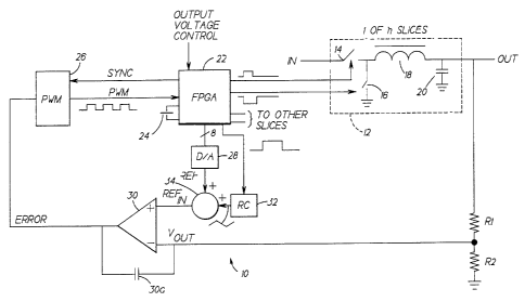
Fig. lA is a block diagram of a multi-slice power converter
having a digital control loop;
Fig. lB is a block diagram of the FPGA circuit of Fig. lA,
wherein Figs. lA and lB are hereinafter referred to
collectively as Fig. l;
2 1 62947
Docket No.: 300-955690-NA 5
PATENT
Fig. 2A is a timing diagram showing the slice phasing for
the converter of Fig. 1;
Fig. 2B is a timing diagram showing the signal timing for
the buck switch and the synchronous rectifier for the
converter of Fig. l;
Figs. 3A and 3B illustrate an exemplary input sinusoid
disturbance and the resulting quantized output,
respectively, and are useful in explaining the invention;
Fig. 4 illustrates a typical quantized pulse width
modulated signal A that transitions between a first pulse
width B and a second pulse width C;
Fig. 5 illustrates a Bode plot for the voltage mode
stabilized converter of Fig. 1;
Fig. 6 illustrates the input noise spectrum for the
converter of Fig. 1; and
Fig. 7 illustrates a satellite communications payload of a
type that benefits from the use of the stabilized converter
of Fig. 1.
DETAILED DESCRIPTION OF THE INVENTION
Referring now to Fig. 1 there is shown a DC-DC power
converter 10 that is constructed and operated in accordance
with this invention. The fundamental topology of the
converter 10 is non-isolated buck. In order to provide a
high current output the converter 10 is preferably
structured with n buck slices 12. In the presently
preferred embodiment five buck slices are used, although
this number is not to be read as a limitation upon the
practice of this invention. In general, n can be any
integer that is equal to or greater than one. The use of
2 lb2947
Docket No.: 300-9S5690-NA 6
PATENT
five slices in the converter 10 enables fault-tolerance,
since if one slice fails (e.g., blows its own fuse) the
remaining four slices are sized so as to continue providing
full power. Each slice 12 is constructed as a buck
converter power stage having a buck MOSFET 14 (illustrated
as a switch), and a second MOSFET 16 that functions as a
synchronous rectifier. Each slice 12 includes gate drivers
(not shown) for the MOSFET switches 14 and 16, an
inductance 18, and a filter capacitor 20. To achieve high
efficiency, the power stage does not use Schottky diode
rectifiers, but instead uses the second MOSFET 16 as a
synchronous rectifier. In order to prevent cross-
conduction, a condition wherein both of the MOSFETs 14 and
16 are on simultaneously, thereby presenting a short to the
input (In) bus, the buck transistor 14 turns on only after
the synchronous rectifier transistor 16 has turned off, and
turns off before the rectifier transistor 16 turns on. Fig.
2B illustrates the time relationship between the gate drive
waveform for the buck MOSFET 14 and the rectifier MOSFET
16. These signals to control the buck transistor 14 and the
rectifier transistor 16 are not merely inverses of each
other, but must involve delays, and thus require two
separate drive signals.
In order to reduce output ripple (which for this embodiment
is preferably less than 50mVpp at 166A to prevent injecting
noise into the antenna load); the slices are phased 360/5
= 72 apart (see Fig. 2A), increasing the ripple frequency
from a fundamental 60kHz to 300kHz. This increased
frequency also reduces stress on the capacitors.
Altogether, a total of 2 x 5 = 10 different control signals
(one each for the MOSFET buck transistor 14 and the MOSFET
synchronous rectifier 16 in each slice 12) are required to
control the power stage.
Generation of the ten control signals using a conventional
analog approach would be complicated. For example, the use
21 62947
Docket No.: 300-955690-NA 7
PATENT
of one-shots would require a moderately large number of
integrated circuits, trimming resistors, low temperature
coefficient capacitors, etc.
In the preferred embodiment of the invention a single
digital integrated circuit is employed to synthesize the
control signals. In the presently preferred embodiment of
this invention the digital integrated circuit is embodied
within a Field Programmable Gate Array (FPGA) 22. In other
embodiments of the invention a plurality of discrete
integrated circuits can be employed instead, and/or a
suitably programmed high speed digital signal processor
could be used to generate the control signals for the
slices 12, as well as to perform the other functions that
are described below. The use of the FPGA is preferred in
that it enables a low cost and simple one chip digital
control circuit to be implemented.
The FPGA 22 drives a 12MHz crystal 24 (period = 83.3 nsec)
from two of its pins, and uses the resulting square wave as
a clock signal. Dividing the 12MHz clock signal by 200
(using a synchronous counter) generates the 60kHz clock
which is used to synchronize (SYNC) an external PWM
integrated circuit 26.
With the PWM signal output from the PWM 26 thus established
at 60kHz, generating the required phasing and delays for
the power stage control signals becomes straightforward: a
first signal reflects exactly the input signal coming from
the PWM 26, and subsequent slices 12, which are delayed
360/5 = 12MHz/(60kHz x 5) = 200 counts/5 = 40 counts, are
generated by FPGA counters 22a, and associated 40 count
delay circuits 22b, that are triggered by the rising and
falling edges of the first PWM signal (see Fig. 2A).
Similarly, the absence of cross-conduction is guaranteed by
forcing the buck transistor 14 and the rectifier transistor
16 of each slice 12 to be delayed on their respective edges
2~ 62947
Docket No.: 300-955690-NA 8
PATENT
by 250nsec = 3 clock counts (see Fig. 2B).
The FPGA 22 also includes an up/down counter 22c and
associated counter control 22d used to program an external
8-bit D/A converter 28, which in turn generates a required
reference voltage (REF) for the PWM 26 via an error
amplifier 30. The error amplifier 30 also receives an input
from a resistor divider comprised of Rl and R2 which are
connected to the output node (OUT) that is coupled in
common to the output of each of the n slices 12. The
voltage that is developed at the junction of Rl and R2
(V~T) is input to the error amplifier 30, and a difference
between this voltage and the reference voltage is input to
the PWM 26 as an error voltage (ERROR) to close the control
loop.
The use of the FPGA 22 causes the control loop to become
irreducibly digital. That is, with the FPGA 22 in the power
converter control loop only certain discrete pulsewidths
are possible. For example, if the output of the PWM 26 is
anywhere between 19.5/12MHz = 1.625~sec and 20.5/12MHz =
1.875~sec, the outputs of the FPGA 22, which generates the
signals which actually control the power stage, are exactly
20/12MHz = 1.750~sec. Thus, only certain discrete
pulsewidths can be obtained, and the pulsewidth of the
signals applied to the power stage (i.e., the slices 12) is
quantized. By contrast, in a conventional analog system any
desired pulsewidth can be generated as a continuous
function.
The quantization of the power stage control signal
pulsewidths leads to the stability concerns that were
discussed previously. To reiterate, there are two types of
stability concerns that arise as a result of the use of the
digital control loop of Fig. 1, in addition to the
conventional analog-type of stability. These stability
concerns relate to: (a) digital oscillations due to noise
2 1 62947
Docket No.: 300-955690-NA 9
PATENT
injection; and (b) oscillations due to a mismatch between
the output voltage setpoint and the available (quantized)
duty cycles. As was previously stated, the first type of
stability concern is independent of the power supply's
operating point; while the second type depends on the input
and output voltages, as well as on the number of possible
duty cycles that are attainable by the PWM signal.
An analysis of these stability concerns is now presented so
as to provide a greater appreciation and understanding of
the benefits that accrue from the use of the teaching of
this invention.
First to be considered analytically is the effect of
moderate size disturbances, i.e., those that are large
enough to cause a change in the duty cycle, but not large
enough to make the above-mentioned analog approximation
valid. In this portion of the analysis the gain and phase
of a sinusoidal disturbance passing through the switching
section of the converter will be considered.
Referring to Fig. 3A, a sinusoid is of such amplitude and
offset that it hits one duty cycle transition level at some
point during its positive swing, and also hits a second
duty cycle transition during its negative swing. It will
become apparent below that this case is generic. The
sinusoid need not be symmetric, that is, it may be above
the high level longer than it is below the low level, or
vice versa. The resulting output is shown in Fig. 3B. It
should be noted the steps shown are not at the switching
frequency: they are instead output voltage responses of the
converter 10 to the sinusoidal disturbance. In fact, it may
be useful to consider these steps as being the output of
the DC transformer of a state-space averaged model. Each
level is characterized by a phase angle of the sinusoid, or
equivalently by a time at which it turns on and off.
Clearly, there is a symmetry around ~/2 and 3~/2 radians
21 62947
Docket No.: 300-955690-NA 10
PATENT
for the high and the low levels, respectively.
The mathematical details of the foregoing are provided in
the Appendix that precedes the claims. To summarize those
results here, in order to determine the transfer function,
the sine wave is injected and the result is determined. Of
interest are only the components at the same frequency as
the injected signal. That is, and just as for analog
stability analyses, the higher frequency harmonics do not
affect stability. Instead, they merely represent the
nonlinearities of the system. If a Fourier representation
of the output is formed, with just the input frequency
retained, it is observed that there is no phase shift
between the input disturbance and the quantized response.
Referring to the origin of the various terms in the
Appendix equation (6), and how they cancel in equation (7),
it is clear that the symmetry of the output piecewise
constant waveform is the same as that of the input
sinusoid. Thus, regardless of the number of levels
crossed, the phase term will remain zero.
Looking next at the amplitude term, we find that the
maximum gain (from the Appendix) is:
Gmax = 2~V/~Va; (13)
and the ratio of the digital to the analog gain is:
Gmax,digital/Gmax,analog = 2/~ < 1. (14)
This is the maximum possible gain for any number of steps;
thus, the digital gain is always less than the gain of the
approximating analog system, and, since the phase shift is
zero, the digital system is always stable if the analog
system is stable. This is an important realization, as will
be evident below.
Although it has been demonstrated that the digital system's
stability is determined by the analog system's stability,
21 62947
Docket No.: 300-955690-NA 11
PATENT
this realization does not bear directly on the problem that
results from digital oscillations that are due to
unachievable duty cycles, rather than loop disturbances.
As was shown above, since the input voltage is a continuous
variable, these oscillations would certainly exist, so it
is necessary to provide circuitry to suppress these
oscillations.
In accordance with an aspect of this invention the FPGA 22
of Fig. 1 includes circuitry (e.g., a divide by 4 counter)
to generate a square wave at 15kHz, i.e., one quarter of
the 60kHz switching frequency. This square wave is then
filtered by an RC network 32 to form a triangle wave, and
this triangle wave is added at node 34 to the DC reference
voltage. The result is the generation of a small ripple
component in the reference voltage (REFjn) for the PWM 26.
The ripple frequency is selected so as to be far higher
than the bandwidth of the converter 10 (e.g., an order of
magnitude higher). As a result, the error amplifier 30
cannot respond to the ripple component. As a result, some
portion of each cycle of the 15kHz ripple causes the duty
cycle generated by the PWM 26 to have a first value, and
the remainder of the ripple cycle causes the duty cycle
generated by the PWM 26 to have a second value.
A slight adjustment of the gain of the error amplifier 30
(at a low frequency) produces a slight adjustment of the
number of PWM pulses that are at the higher vs. the lower
duty cycle. Thus, at the relatively low frequency of the
converter bandwidth, an effectively continuous adjustment
of the error amplifier 30 is possible, yielding a
substantially continuous adjustment of the output voltage.
This then eliminates a possibility of digital oscillation,
since this dithering of the reference voltage with the
15kHz signal produces, in effect, a subdivision of the
possible duty cycles possible (by a factor of
21 62947
Docket No.: 300-955690-NA 12
PATENT
15kHz/bandwidth). The dither frequency component also does
not appear to any significant degree in the output or the
input of the converter 10, since its frequency is well
beyond the input and output LC filter frequencies.
In accordance with this aspect of the invention it has been
shown that the oscillation due to unachievable duty cycles
is suppressed by adding in a predetermined amount of dither
to the reference voltage to the PWM 26.
A 1300W breadboard using the FPGA 12 as described herein
was constructed, stabilized and tested. Fig. 4 shows the
output drive signal from the FPGA 12 that goes directly ~o
the power stages. For the waveform shown in Fig. 4 the
reference voltage was driven with a superimposed small ac
voltage, forcing the duty cycle to continually adjust. In
a conventional analog system, this would result in a
continuous spectrum of duty cycles. However, for the
digital control system only a discrete number of duty
cycles are possible (here, two designated as B and C), with
the two duty cycles being separated by (l/12MHz) = 83.3
nsec.
Fig. 5 shows a Bode plot for the (voltage-modej converter
10. Stabilization is shown to be successful, with 45 of
phase margin at 500Hz. The low bandwidth was selected for
other, system reasons, and was not necessitated by the
digital loop. The compensation (30a in Fig. 1) for the
error amplifier 30 was comprised of a single pole at the
origin.
Fig. 6 illustrates the input noise spectrum of the
converter 10. Only background noise is visible at 300kHz,
the overall switching frequency, indicating the correct
phasing of the slices 12. Peaks of about 20dB above
background are visible at 60kHz and its third harmonic
180kHz. This is believed to be due to imbalances in the
21 62947
Docket No.: 300-955690-NA 13
PATENT
power distribution system, causing some slices to carry
more power than others (the input current can be as high as
lOOA in the illustrated embodiment of the converter 10).
Finally, a peak is visible at 15kHz, the dithering
frequency. Aside from increasing the size of the input
filter, this peak can also be reduced by decreasing the
amount of dither. However, this reduction would also reduce
the margin for stability against unachievable duty cycle
oscillations.
It has been shown that the use of the FPGA 22 to generate
the drive signals to the power stage of the converter 10
results in the control loop becoming irreducibly digital.
Because the duty cycle can only have one of a certain small
group of values, two types of stability questions arise:
(a) the stability of the control loop against signals that
cause the duty cycle to cycle between two discrete values;
and (b) the stability against oscillations caused by the
control loop attempting to reach a duty cycle that is not
a possible value. It has been shown above that the first
type of oscillation will not occur if the control loop is
stable as an analog system; and second, that the addition
of a small amount of high-frequency dither to the reference
voltage of the PWM 26 is sufficient to guarantee that the
second type of oscillation is adequately controlled.
Having described in detail the presently preferred
embodiment of this invention, reference is now made to Fig.
7 for illustrating a generic model for a payload of a
communications satellite la of a type to which this
invention can be applied. A constellation of 48 such
satellites enables users to make phone calls anywhere in
the world.
More particularly, Fig. 7 illustrates a satellite
transponder lb configured for full duplex communication.
The communications payload includes one or more such
21 62947
Docket No.: 300-955690-NA 14
PATENT
transponders having a plurality of antennas 2 to receive
signals from the earth's surface, low noise amplifiers 3,
frequency shifters or converters 4 comprised of a local
oscillator and a mixer, followed by amplifiers 5, high
power amplifiers 6 and transmitting antennas 7. Filters 8
are also included to pass desired in-band signals and
reject unwanted out-of-band noise signals. One transponder
receives signals from user terminals 9a, frequency shifts
the received user signals, and transmits the frequency
shifted signals to a ground station, such as a gateway 9b
that is connected to the public switched telephone network
(PSTN). A second transponder receives signals from one or
more of the gateways 9b, frequency shifts the received
signals, and transmits the frequency shifted signals to the
user terminals 9b. In this manner a full duplex
communication path (voice and/or data) is established
between user terminals and terminals connected to the PSTN.
By example, the user terminals 9a (fixed or mobile) are
capable of operating in a full duplex mode and communicate
via, by example, L-band RF links (uplink) and S-band RF
links (downlink) through the return and forward satellite
transponders, respectively. Uplink L-band RF links may
operate within a frequency range of 1.61 GHz to 1.6265 GHz,
bandwidth I6.5 MHz, and are preferably modulated with voice
signals and/or digital signals in accordance with a spread
spectrum technique. Downlink S-band RF links may operate
within a frequency range of 2.4835 GHz to 2.5 GHz,
bandwidth 16.5 MHz. The gateway 9b may communicate with the
satellite la via receive antenna 2b and transmit antenna 7a
with, by example, a full duplex C-band RF link that may
operate within a range of frequencies centered on 5 GHz.
The C-band RF links bi-directionally convey communication
feeder links, and also convey satellite commands (forward
link) and receive telemetry information (return link). The
L-band and the S-band satellite antennas 2a and 7b,
respectively, are multiple beam (preferably 16 beam)
2 1 62947
Docket No.: 300-955690-NA 15
PATENT
antennas that provide earth coverage within an associated
service region. The L-band and S-band satellite antennas 2a
and 7b are preferably congruent with one another. As an
example, a total of approximately 3000 full duplex
communications may occur through a given one of the
satellites. Two or more satellites la may each convey the
same communication between a given user terminal 9a and one
of the gateways 9b by the use of spread spectrum
techniques. This mode of operation thus provides for
diversity combining at the respective receivers, leading to
an increased resistance to fading and facilitating the
implementation of a soft handoff procedure.
It is pointed out that all of the frequencies, bandwidths
and the like that are described above are representative of
but one particular system. Other frequencies and bands of
frequencies may be used with no change in the principles
being discussed. As but one example, the feeder links
between the gateway 9b and the satellite la may use
frequencies in a band other than the C-band, for example
the Ku or Ka bands.
It can be appreciated that the S-Band transmitter 6 is the
highest power element on the spacecraft. The S-Band
transmitter is preferably powered by the DC-DC converter 10
as described in detail above.
The output power of the S-Band transmitter power amplifier
6 is determined by its supply voltage, and so to control
the S-Band transmitter power, the power converter 10 has an
adjustable output voltage that ranges from 2V at 66A to
8.3V at 166A. A signal (not shown in Fig. l) is input to
the FPGA 22 to control the magnitude of the digitally
programmed REF voltage output from the D/A 28 and, thus, to
control the output power of the converter 10 and the output
power of the S-Band transmitter power amplifier 6.
2 1 62947
Docket No.: 300-955690-NA 16
PATENT
With an input voltage range of 14-23V (derived from on-
board solar cells or batteries), high efficiency is
required in order to make the satellite power budget
practical. In addition, the converter 10 should be small,
lightweight and fault-tolerant, since it is intended to
operate in space.
The converter 10 of this invention provides the necessary
controllable output power to the S-band transmitter
amplifier 6, and does so employing the digital control loop
implemented by the FPGA 12 and the stabilization techniques
that were detailed above.
It should be realized that a number of modifications can be
made to the presently preferred embodiment of this
invention. By example, the dither signal generated by the
FPGA 12 can instead be incorporated into the digital data
that drives the D/A 28, thereby eliminating the requirement
to provide the RC network 32 and the summing node 34. This
embodiment assumes that the D/A 28 has sufficient
resolution. Furthermore, the teaching of this invention
applies as well to power converters that use fixed
reference voltages, as opposed to the programmable
(variable) reference voltage output by the D/A 28.
Further by example, other switching frequencies and other
types of converter topologies can be employed.
Also by example, the synchronous rectifier 16 can be
replaced by a conventional Schottky-type rectifier, thereby
eliminating one of the required control signals per slice.
In general, the dither signal is a periodic signal having,
by example, a sinusoidal or a triangular wave-shape. A
minimum amplitude for the dither signal is one that covers
at least two quantization steps, while a maximum amplitude
is generally set by system noise requirements.
2 1 62947
Docket No.: 300-955690-NA 17
PATENT
The dither signal has a frequency that is less than the PWM
frequency and greater than a bandwidth frequency of the
converter. The dither signal functions to effectively
increase the number of possible duty cycles by a factor
given by the ratio of the dither frequency to the bandwidth
frequency. In the embodiment of the invention that was
described in detail above the dither signal frequency is
one quarter of the PWM frequency and at least an order of
magnitude greater than the bandwidth frequency.
While the invention has been particularly shown and
described with respect to a preferred embodiment thereof,
it will be understood by those skilled in the art that
changes in form and details may be made therein without
departing from the scope and spirit of the invention.
21 62947
Docket No.: 300-955690-NA 18
PATENT
APPENDIX
In the following a sine wave is injected and the output of
the quantization process is observed at the same frequency.
In equations, then, the sine is
V= VO+ Vasint~t) (1)
where f = ~ / (2 ~) = 1 / T is the frequency of the
disturbance. The time when the sine wave reaches the level
Vh is given by solving (1):
td = T sin~l ( Vh - VO) (2)
The time when it recrosses is (T / 2) - td, from symmetry.
Similarly, the time when the sine crosses the level Vl is
te = T sin~l( Vl - VO
and the recrossing time is (3 T / 2) - te.
Now, the output, f(t), has levels Vl, and Vl _ ~V (see
Figure 3). Since it is periodic, it can be expressed in a
Fourier series,
f( t) = a2 + ~ (An cos 2 ~T t + Bn sin 2 ~T t) (4)
As discussed above, we are only interested in the
components at the frequency of the injected signal. Thus,
we approximate
f(t) z Al cos 2 T t ~ Bl sin 2 T t (5)
21 62947
Docket No.: 300-955690-NA 19
PATENT
To find the Fourier coefficient, we have the following:
Al = --T I f(t) cos 2 ~ t dt = 2 [tJd
O T T o
2 T t dt + 2 1 (Vl + ~V~ cos 2 T t dt + T Vl cos
2 n t dt + 2 r; (Vl - /~V) cos T 2
Vl cos ~ T t d t]
(6)
The cosines all evaluate to sines, and substituting we find
Al = ~ [Vl sin T ~ (Vl + ~V) sin (~ - T
- (V1 + ~ ~ sin 2 ~ td + Vl sin 2 ~ te _ Vl sin
_ 2 ~Ttd) + (Vl - ~V) sin (3 ~ 2 J~Tte) - (Vl - ~1
sin 2 ~ te _ Vl sin (3 ~ _ 2 1~ te) ]
(7)
Making the obvious cancellations, and using the fact that
sin(3~ -~) = sin(~ - ~) = sin(~), we find that A1 = 0,
which is to say, since A multiplies the cosine term in the
Fourier expansion, there is no phase shift.
Looking at the origin of the various terms in (6) and at
how they cancel in (7), it is obvious that the symmetry of
the output piecewise constant waveform is the same as that
2 1 62947
Docket No.: 300-955690-NA 20
PATENT
of the input sinusoid. Thus, regardless of the number of
levels crossed, the Al term will remain zero.
Evaluating the Bl term,
Bl = 2 I f ( t) sin 2 T t dt = 2T [ J Vl
T _ td
sin 2 T dt + J (Vl + ~ sin 2 T t dt
te 3 T _ te
+0 T td Vl sinT dt + 2 J
2 te
T dt 3 T t Vl sin 2 t dt]
(8)
Again, the sines become -cosines, yielding
Bl = - 1 [ Vl cos 2 T~T td + ( Vl + ~\V) cos
_ 2 ~ td ) - ( Vl + ~ cos 2 ~ td + Vl cos ~T
- Vl cos (~ _ 2 ~ td )
+ (V1 - ~ ~ cos (3 ~ ~ T ) -
(Vl - ~V) cos 2 ~Tte _ Vl cos (3 ~ _ 2 ~Tte) ~
(9)
There are again cancellations, and this time cos(3~
cos (7r -- c~ cos (c~):
21 62947
Docket No.: 300-955690-NA 21
PATENT
Bl = - 1 [-2 ~V cos 2 ~ td ~ 2 ~ V cos 2 T ] (10)
We can now substitute in the expressions for td and te, (2)
and (3),
~ Va Va
2 ~V Vh -VO 1/2 Vl - VO 1/2 (11)
This is the term multiplying the sine term; since the input
was of amplitude Va, the gain of the system is
2 ~ V Vh VO 1/2 Vl - VO 1/2
Examination of the two terms in G reveals that the positive
term comes from the crossing of the upper transition level,
and the negative term from the lower transition level.
Evidently, there will always be a positive term for each
transition that occurs above the average of the input
sinusoid (VO) and a negative term for each transition
below; and the difference between the number of positives
21 62947
Docket No.: 300-955690-NA 22
PATENT
and negatives must be either zero or one. That is, if the
sinusoidal disturbance crosses three levels, for example,
there must either be two positive terms and one negative
term in G, or else one positive term and two negative
terms.
This being the case, the maximum gain will occur if: 1) V0
= Vh, which is to say that one of the transition levels
occurs at the average value of the sinusoid; and 2) (Vl -
Vo) / Va = 1, which is to say that another transition
occurs at exactly the peak of the sinusoid. With these two
conditions, the expression in the curly braces = 1, and
Gmax = ~ Va (13)
Now in the continuous (analog) case, and assuming a sine
wave duty cycle, a sine wave output voltage is obtained.
If the duty cycle varies from 0 to 1, the output varies
from 0 to Vin; thus the gain is Vin. Since the step, ~V,
is Vin times the change in duty cycle, Gmax differs from
the continuous case by only the numerical factor
Gmax, digi tal = 2 ( 14 )
Gmax, analog
which is less than 1.