Note: Descriptions are shown in the official language in which they were submitted.
WO 94/28508 2 f 6 3 0 2 4 PcT~s94/oæ38
1
METHOD AND APPARATUS FOR STORING COMPRESSED DATA FOR
SUBSEQUENT PRESENTATION ON AN ACTIVE ADDRESSED DISPLAY
Field of the Invention
This invention relates in general to data compression techniques,
and more specifically to dah ~u~ u~ ion in an active addressed display
System.
Background of the Invention
An example of a direct multiplexed, rms (root mean square)
uulldillg electronic display is the well-known liquid crystal display
(LCD). In such a display, a nematic liquid crystal material is positioned
between hwo parallel glass plates having electrodes applied to each surface
in contact with the liquid crystal material. The electrodes typically are
arranged in vertical columns on one plate and hnri7-)nt~1 rows on the
other plate for driving a picture element (pixel) wherever a column and
row electrode overlap.
In rms-rPqr~ in~ displays, the optical state of a pixel is s--hct~nh'~lly
JUll~l;Vt~ to the square of the voltage applied to the pixel, i.e., the
difference in the voltages applied to the electrodes on the opposite sides of
the pixel. LCDs have an inherent time constant that ~h~r~ct~ri7Ps the time
required for the optical state of a pixel to retum to an equilibrium state
after the optical state has been modified by changing the voltage applied to
the pixel. Recent tPrhn~ gir~l advances have produced LCDs with time
constants (d~lulv~ll~ly 16.7 millicP~r~nrls) c~lululu~ g the frame period
used in many video displays. Such a short time constant allows the LCD
to respond quickly and is especially advantageous for depicting motion
without noticeable smearing or flickering of the displayed image.
Cul~v~nliul~al direct multiplexed addressing methods for LCDs
encounter a problem when the display time constant approaches the
frame period. The problem occurs because ~:ullv~llLiùllal direct
multiplexed ~ 3rPcsin~ methods subject each pixel to a short duration
"selection" pulse once per frame. The voltage level of the selectiûn pulse
is typically 7-13 times higher than the rms voltages averaged over the
frame period. The optical state of a pixel in an LCD having a ~Ft time
WO 94/28508 - PCT/US94104238
2--- 2 1 6302~ --
constant tends to retum towards an equilibrium state between selection
pulses, resulting in lowered image contrast, because the human eye
integrates the resultant brightness transients at a perceived int~rm~ t~
level. In addition, the high level of the selection pulse can cause
5 alignment instabilities in some types of LCDs.
To overcome the above-described problems, an "active addressing"
method for driving rms responding electronic displays has been
developed. The active addressing method (-r1ntinll0u~ily drives the row
electrodes with signals ~u~ ul;~il,g a train of periodic pulses having a
10 common period T corresponding to the frame period. The row signals are
independent of the image to be displayed and preferably are orthogonal
and nnrm~i7f~rl i.e., orthnn~-r nAI The term "orthogonal" denotes that, if
the amplitude of a signal applied to one of the rows is multiplied by the
Annrlihl~lP of a signal applied to another one of the rows, the integral of
15 this product over the frame period is zero. The term "nnr~n~li7f~cl"
denotes that all the row signals have the same rms volhge intPgrA~d over
the frame period T.
During each frame period a plurality of signals for the column
electrodes are calculated and generated from the collective state of the
20 pixels in each of the columns. The column voltage at any time t during
the frame period is lulu~o~iul~al to the sum obtained by r~n~ Prin~ each
pixel in the column, multiplying a "pixel value" l~ lillg the optical
state (either -1 for fully "on", +1 for fully "off", or values between -1 and
+1 for proportionally corresponding gray shades) of the pixel by the value
25 of that pixel's row signal at time t, and adding the products obtained
thereby to the sum.
If driven in the active ~i(1rP~cin~ manner described above, it can be
shown ~ Ally that there is applied to each pixel of the display an
rms voltage averaged over the frame period, and that the rms voltage is
30 lululJvlliulldl to the pixel value for the frame. The advantage of active
addressing is that it restores high contrast to the displayed image because,
instead of applying a single, high level selection pulse to each pixel during
the frame period, active addressing applies a plurality of much lower level
(2-5 times the rms voltage) selection pulses spread ~ uu~ ou~ the frame
35 period. In addition, the much lower level of the selection pulses
subshntially reduces the probability of alignment instabilities. As a result,
utilizing active addressing methods, rms-responding displays, such as
WO 941~8508 2 1 6 3 0 2 ~ PCT/US94/04238
3 -
LCDs used in laptop ~UllIIJU~ , can display image data at video speeds
without smearing or flickering. ~ditinn~lly, LCDs driven with active
addressing methods can display image data having multiple shades
without the contrast problems present in LCDs driven with conventional
5 multiplexed addressing methods.
A drawback to utilizing active addressing results from the large
number of ~ tinnc required to generate column and row signals for
driving an rms-responding display. For example, a gray scale display
having 480 rows and 640 columns and a frame rate of 60 frames per second
10 requires just under ten billion ~lc~ tlnnC per second. While it is, of
course, possible to perform ~ tinnc at this rate, such complex, rapidly
p~lrulll-ed fAl~ tinnc 11~ a large amount of power ~ul~su~ uLiull.
In portable, battery powered devices, such as laptop ~UllllUU~t:la and radio
receivers, the power LUllsull-luliul- issue is particularly important because
15 battery life is a primary design rnn~ r~tinn
Thus, what is needed is a method and apparatus for ",;..;",;,;"~ the
power ~ul~ull.lu~iul. required to display image data on an active-addressed
display.
Summary of the Invention
According to an aspect of the present invention, a method for
~UllI~ illg data in an electronic device having an active-addressed
display comprises the step of receiving image data. The method further
25 comprises the step of ~UIllpl..,J.llg the image data in a two-~]i",.-": ."~1
..ll~r",...~ ". utilizing a plurality of orthogonal functions, thereby
alillg ~ullllulca~d data. Sub~eulu~l~Lly, a set of column values in
accordance with active-addressing techniques is generated by performing a
one--li",~ ".".r",."~li.." of the ~ull-lul~:,D~d data utilizing the
30 plurality of orthogonal functions.
According to another aspect of the present invention, a method for
Ulll~ illg data s~ æ~ l to displaying the data in an electronic device
having an active-addressed display comprises the steps of receiving image
data and ~l~nPri~ting a set of column values in accordance with active
35 ~tlr~ccin~ techniques by one-.l;",t~"-: ",~lly l,,.,,~r,,,...i,.~ the image data
utilizing a plurality of orthogonal functions. The method further
comprises the step of driving columns of the active-addressed display with
WO 94/28508 ~ 2 1 6 3 û 2 4 PCT/US94104238
4 . .- ~
analog voltages corresponding to the set of column values. The image
data is then ~u~ d by using a compression method in which the set
of column values is one-~limPnci~-n ~lly trAnqfnrmPd utilizing the plurality
of orthogonal functions, wherein the compression method results in
5 ~ul~lulc~cd data which is ~ub~e~lucllLly stored.
According to still another aspect of the present invention, an
electronic device for driving an active-addressed display comprises a data
port for receiving image data and ~U~II,UlC~illg circuitry coupled to the data
port for generating ~ull~cs~ed data by ~ull-lu~c.,..illg the image data using a
10 method in which the image data is two-rlimPn~inn~lly ll,."~rl,."lP,l
utilizing a plurality of orthogonal functions. The electronic device further
comprises Ll,."~.r."...i..~ circuitry coupled to the ~Ulll~lc~illg circuitry for illg a one-~limPn~i?n~l L~ r.~ i..,. of the ~u~ lcs~cd data
utilizing the plurality of orthogonal functions to generate a set of column
15 values. Column drivers coupled to the ~ r~ circuitry and the
active-addressed display drive columns of the active-addressed display
with a first set of analo~ voltages corresponding to the set of column
values.
Brief Description of the Drawings
FIG. 1 is a front orthographic view of a portion of a ~ullvcllliul~dl
liquid crystal display.
FIG. 2 is an u~ cross-section view along line 2-2 of FIG. 1
25 of the conventional liquid crystal display.
FrG. 3 is a matrix of Walsh functions in accordance with the present
invention.
FIG. 4 depicts Walsh functions in a.~u..ld l.e with the present
invention.
FIG. 5 is an electrical block diagram of an electronic device for
generating signals to activc ~rirPC~ the liquid crystal display of FIG. 1 in
accordance with the present invention.
FIG. 6 is a flowchart depicting the operation of a controller included
in the electronic device of FIG. 5 in accordance with the present invention.
WO 94128508 2 1 ~ 3 0 2 ~ PCT/US94/0~238
5
Description of a Preferred Embodiment
Referring to FlGs. 1 and 2, orthographic front and cross-section
'' views of a portion of a conventional liquid crystal display (LCD) 100 depict
first and second Lldl~al~ l substrates 102, 206 having a space
Lll.~ Lvv~l~ filled with a layer of liquid crystal material 202. A perimeter
seal 204 prevents the liquid crystal material from escaping from the LCD
100. The LCD 100 further includes a plurality of llall~al~lL electrodes
~Ulll,Ul;sil~g row electrodes 106 posi~iul,ed on the second
10 substrate 206 and column electrodes 104 po~iliul~ed on the first ~
substrate 102. At each poimt at which a column electrode 104 overlaps a
row electrode 106, such as the overlap 108, voltages âpplied to the
uv~lla~ lg electrodes 104,106 can control the optical state of the liquid
crystal material 202 Ll~ b~ .l, thus formmg a controllable picture
15 element, hereafter referred to as a "pixel". While an LCD is the preferred
display element in accordance with the preferred PmhoflimPnt of the
present invention, it will be d~ Lial~d that other types of display
elements may be used as well, provided that such other types of display
elements exhibit optical ~h~r~CtPristifc l~ JUli~iVt~ to the square of the
20 voltage applied to each pixel, similar to the root mean square (rms)
response of an LCD.
FlGs. 3 and 4 depict an eight-by-eight (third order) matrix of Walsh
functions 300 and the corresponding Walsh waves 4ûO in accordance with
the preferred Pmhoflim~nt of the present invention. Walsh functions are
25 both orthogonal and nnrm~li7Prl, i.e., u~ l, and are therefore
preferable for use in an active-addressed display system, as briefly
discussed in the Background of the Invention herein above. It may be
a~ .ial~d by one of ordinary skill in the art that other classes of
functions, such as Pseudo Random Binary Sequence (PRBS) functions or
30 Direct Cosine Transform (DCT) functions, may also be utilized m active-
rpccPrl display systems.
When Walsh functions are used in an active-addressed display
system, voltages having levels l~ L~:~ by the Walsh waves 400 are
uniquely applied to a selected plurality of electrodes of the LCD 100. For
35 example, the Walsh waves 404, 406, and 408 could be applied to the first
(U~p~ V~L), second and third row electrodes 106, ~ ye~Livt:ly~ and so on.
In this manner, each of the Walsh waves 400 would be applied uniquely to
WO 94/28508 2 1 6 3 0 2 4 PCTIVS94/04238
~6 "
a corresponding one of the row electrodes 106. It is preferable not to use
the Walsh wave 402 in an LCD application because the Walsh wave 402
would bias the LCD 100 with an umdesirable DC voltage.
It is of interest to note that the values of the Walsh waves 400 are
5 constant during each time slot t. The duration of the time slot t for the
eight Walsh waves 4Q0 is one-eighth of the duration of one complete cycle
of Walsh waves 400 from start 410 to finish 412. When using Walsh
waves for actively addressing a display, the duration of one complete cycle
of the Walsh waves 400 is set equal to the frame duration, i.e., the time to
10 receive one complete set of data for controlling all the pixels 108 of the
LCD 100. The eight Walsh waves 400 are capable of uniquely driving up to
eight row electrodes 106 (seven if the Walsh wave 402 is not used). It will
be a~le~id~t:d that a practical display has many more rows. For example,
displays having four-hundred-eight rows and six-hundred-forty columns
15 are widely used today in laptop ~u~ uu~ . Because Walsh f mction
mahrices are available m complete sets rlr-tr-rminr~d by powers of two, and
because the orthr~nrrm~lity Ic~uluil~ for active a~l.lrr~ does not
allow more than one electrode to be driven from each Walsh wave, a five-
hundred-twelve by five-hundred-twelve (29 x 29) Walsh function matrix
20 would be required to drive a display having four-humdred-eighty row
electrodes 106. For this case, the duration of the time slot t is 1/512 of the
frame duration. Four-hundred-eight Walsh waves would be used to drive
the four-hundred-eighty row electrodes 106, while the l~lllaillillg thirty-
two, preferably including the first Walsh wave 402 having a DC bias,
25 would be unused.
It will be dlu~l~-ia~:d that driving a display, such as the LCD 100
(FIG. 1), in accordance with the active-addressing technique as described
above involves a large number of r:~lr~ hr~nq that must be rapidly
performed, thereby ~ a large amount of power ~u~u~ ion.
30 In portable devices which are battery powered, the power ~u~-~u--llu~ioll is a
very important issue because of the limited capacity of the battery.
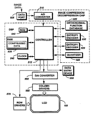
Referring next to FIG. 5, an electrical block diagram of an electronic
device 500 includmg an active-addressed display, such as the LCD 100, is
shown. The electronic device 500, e.g., a portable laptop computer or a
35 paging receiver, comprises a data port 505 for receiving image data from a
video source (not shown). The data port 505 may be, for example, a
rr~mmllnir~tirm bus, a floppy drive for reading image data from diskettes,
WO 94/28C08 2 1 6 ~ 0 2 4 . PCT~S94/04238
or, in the case of a paging receiver, receiving circuitry for recovering image
data from a radio frequency (RF) signal. The electronic device 500 further
comprises an analog-to-digital (A/D) converter 510 for converting the
analog image data values to digital image data values, which aK provided
5 to a controller 515 for ~ r."".~ the image data into another domain,
as will be explained in greater detail below. The resolution and range of
the A/D converter 510 is ~lPtprmine~l by the desired image to be displayed
on the LCD 100. For instance, if the pixels 108 of the LCD 100 are to be
either fully "on" or fully "off", the A/D converter 510 may convert the
10 image data to binary data, wherein -1 lLyll~Selll:) a fully on pixel and +1
lL~ LL~ a fully off pixel. If gray shades are also to be displayed on the
LCD 100, the A/D converter 510 may generate values between -1 and +1 for
the gray shades. It will be . e~ l that the A/D converter 510 may not
be necessary if digital image data is received by the data port 505.
Coupled to the controller 515 is an or~hnn~rmAI function database
520 for storing a plurality of functions, which are orthogonal and
preferably nnrmAli7Pf1, in the form of an orthnnnrmAI matrix, the nu~nber
of rows of which are preferably greater than or equal to the number of
rows included in the LCD 100. The orthnnormAI matrix may be, for
20 example, the Walsh function matrix 300 (FIG. 3), although matrices of
other orthnnnrmAI functions, such as DCT or PRBS functions, may be
used as well.
In accordance with the present invention, the "lll.. ~..... ~l matrix
is utilized by the controller 515 in L.,...~.~....;.l~ the iInage data upon
25 reception. When the image data is received, the controller 515 performs a
two-~li...~..~i...~l ~,,...~r~ .." of the image data utilizing the
orthonnrmAl matrix to result in two-~imPn~;nnAIIy l.. !.~.. ",~d image
data. By way of example, the two-,li",~"~;.."~l l,,.~,,~r.,. ",~I;..n can be
Irrl~mrli.chPd utilizing a Fast Fourier Transform A1~nrithm, or
30 mnrlifi~Atinn thereof, or a Fast Walsh Transform, although many other
fast, efficient Al~nrithmc can be al~ aLiv~:ly utilized. One such algorithm
involves the use of matrix multiplication and carL be ~ s~ d by the
following equation:
I2D = M " I ~ OM,
wo 94/28508 --- - 2 1 6 3 0 2 4 PCTIUS9410n38
wherein I2D 1~ 11L~ the two-dimPn~ n~lly Ll~l-s~ulllled image data, I
L~ the image data, and OM r~ , the orthnnrlrn-~l matrix
stored in the-u.~ ",l" ~ ~l function database 520. It will be ~ id~t~d
that, when matrix multiplication is utilized, the order of the terms in the
5 above-recited equation cannot be varied.
Further coupled to the controller 515 is a quantizer 525, which
quantizes, in a ~ullv~llLiul~al manner, the two-.l;l.. ~ lly L1,.11C~.. P~
image data to a closest of a number of prPdPtPrminPd levels. An entropy
encoder 530 coupled to the controller 515 is employed to compress the
10 quantized data utilizing one of several well known entropy encoding
schemes, such as Huffman coding, in which the values of the quantized
data are encoded depending upon the probability of orr-lrrPnrP According
to the present invention, the electronic device 500 further includes a
memory device, such as a random access memory (RAM) 535, for storing
15 the l Ulll~ el.l data.
In this manner, image data received by the electronic device 500 is
~:ulllt~ d prior to storage, thereby .. ~.. ;.. ~ Iess space in memory.
The storage of ~ulllL~l.s..~l image data, rather than the image data itself, is
especially advantageous when the electronic device 500 is a portable
20 device, such as a laptop computer, because market trends have dictated
that portable devices, which are often carried by a user, be designed as
small and li~ ..;gl~l as possible. Therefore, with this goal in mind, the
size of ulll~Ull~llL~, such as memory, mcluded in a portable device is also
limited.
Preferably, the electronic device 500 further comprises, in addition
to the RAM 535, a read only memory (ROM) 540, which stores subroutines
executed by the controller 515 during operation of the electronic device
500, and a clock 545, which generates timrng signals for use in system
timing. ~fll1itinn~lly, a data entry device 550 may be coupled to the
controller 515. When the electronic device 500 is a laptop computer, for
instance, the data entry device 550 may comprise a keyboard, whereas,
when the electronic device 500 is a paging receiver, user-accessible
controls, rather than a keyboard, may be coupled to the controller 515.
In accordance with the present invention, the image data can be
displayed dllllllll~lil ,.lly, or the data entry device 550 can be used to rnputrrlmm~nd~i directing the controller 515 to present the image data. When
so directed, the controller 515 operates on the ~Ulll~Jle~ li data to generate
WO 94128508 2 1 6 3 0 2 4 PCT/US94/04238
9
signals suihble for active-addressing the LCD 100. More specifically, an
entropy decoder 555 is employed to decode the ~u~ ss~d data, resulting
in the two~ llr,.~ lly l".".~...,...~.l image data which has been
previously quantized. This data can be easily and quickly l.,."cr~ 1 into
5 signals for active-addressing columns of the LCD 100 by p~lrul~ g a one-
.1;,.~..~; ".~1 inverse ~ ...".~li..., of the data. It will be alu~ id~d by
one of ordinary skill in the art that the ~lf~ tinnc are further simplified
when it is !~ g~ that an orthnnnrm~l matrix, i.e., a separable and
symmetric matrix, is equal to its mverse, i.e., OM = 1/OM. Therefore,
10 because the orthnnnrm~l matrix stored in the orthnnnrm~l function
database 520 was previously utilized in the data ~UIll~l~S~;Ull process, the
same ul ~ l matrix can be utilized by the controller 515 to perhrm
a one-~lim~n.cinn~l trAncform~tinn, e.g., a Walsh Transform, rather than a
one-ll;.. r.. r.;.. ~l inverse l,.~ r.. ~1i.. When matrix multiplication is
15 used, this process is illllctr~tP~I by the following equation-
CV=IlD=I,D~OM,
wherem kD is the two-.]i..... ~.. ~;.. ~lly l".l-~r,.. ~(l image data that has20 been quantized, OM is the ~lll.. ~.. ~.. ~l matrix, and I1D is the resulting
one-~limPncinn~lly l.r,.~r.. ~.~ image data, which is equivalent to
column values (CV) suitable for active-addressing the columns of the LCD
100.
As briefly described herein above in the Background of the
25 Invention, the rûw signals for driving the rows of the LCD 100 are signals
derived from orthnnnrm~l functions independent of the image data. The
column signals, i.e., analog voltages corresponding to the column values,
for driving the columns of the LCD 100 are linear ~ulllbillaliulls of all row
signals and the image data and can be generated by one-11imf~ncinnolly
30 11.-l.`.~ll'.ll;l-~ the image data utilizing the orthnnnrm~l functions.
Therefore, it will be a~ul~ial~d that the column values generated by one-
~limf~nginn~lly Llal~ru~ lg the quantized data are already in a form
suitable for active-addressing the columns of the LCD. As a result, the
electronic device 500 ~ullvt~ llly avoids having to de~ulll~ the stored
35 data, which has been ~l~vio~ y ~ulll~ d for storage. The electronic
device 500 further avoids the necessity of gPn.~r~tin~ column values
directly from the image data each time the image data is to be displayed.
WO 9412850R .2 1 6 3 0 2 4 PCTIUS94/04~38
` 10 -
Instead, the electronic device 500 simply performs the one-llimPncinn~ltransform on the Lulllult aa~d data when it is to be displayed.
In ~ullvt:llL;ullal devices, on the other hand, data that is Lu~ a,ed
and stored in memory must be de.u.."u,t:a,~d, which involves complex
5 ~ Alr~ tinnc, before it can be displayed. ~ itic)n~lly~ if a display in the
device is to be active-addressed, the device also generates, in a
~ul~v~ iu~al manner, the column signals for driving columns of the
display. As a result, ~ul~v~llliulldl devices must include a large amount of
complex circuitry which requires a corresponding large amount of current
10 for operation. Therefore, ~:ullv~ iu~al methods for CUlllplt~aa;Ull,
de.ullllu.~,a;u.., and suba~ulu~lll display of image data may not be suitable
for use in portable devices, which are typically powered by a low capacity
battery.
One of ordinary skill in the art will recognize that the electronic
device 500 according to the present invention exploits the cimil~ritiPc
between data ~Ulll~ aiUII and active addressrng to reduce the number
and ~ull~ ily of ~ tinnc for displaying ~u.ll~ a~d image dah,
thereby nP.,~ a smaller amount of power l.:Ull~UlllU~iUII than
~ul~v~liul~al devices. As a result, the battery life of the electronic device
500 may be longer than that of a battery powering a ~ullv~ iulldl device
which displays ~ulll~l~aa~d data utilizrng active addressing techniques.
As shown m FIG. 5, the electronic device 500 further comprises a
digital-to-analog (D/A) converter 560 coupled to the controller 515 for
converting the column values to analog voltages and column drivers 565
coupled to the D/A converter 560 for driving the columns of the LCD 100
with the analog voltages, i.e., column signals. A~l~litinn~lly, row drivers
570 are employed to drive the rows of the LCD 100 with analog voltages,
i.e. row signals, ~Ull~:~t,Ull-lillg to the u~ functions.
The controller 515, the ROM 540, the RAM 535, and the clock 545
can be implemented by using a suitably ,u~uE;l~ullllle~ digital signal
processor (DSP), such as the DSP 56000~ ., . . t,.. ~ d by Motorola, Inc. of
Schaumburg, Illinois, although other integr?tPd or hard-wired circuihy
that is capable of u..ru....i~-g equivalent operations may be alL~l.ld~iv~ly
utilized. The A/D converter 510, the orthnnnrTn~l function database 520,
35 the entropy decoder 530, the entropy decoder 555, and the quantizer 525
can be ill.pl~ d using an image ~ullly~ iull/de~ulll~ ion chip,
such as the model no. CL550-30 chip m~nllf?chlred by C-Cube
WO 94128~08 2 1 6 3 ~ 2 4 PCTIUS9-/04238
of San Jose, Califomia. ~ itinnAlly, the D/A converter 560,
the column drivers 565, and the row drivers 570 can be iu.~ enl~v
using the following conventional elements:
5 ~m~ Ivln~l No. Ivlanl~f~tllr~r
D/A converter 560 CXD1178Q Sony Cul~vldLiul-
column drivers 565 SED1779DOA Seiko Epson Corp.
row drivers 570 SED1704 Seiko Epson Corp.
It will be l-.v~ e.'i by one of ordinary skill in the art that, when
gray scale or color images are to be displayed, the electronic device 500
may, when necessary, further include means for i-alfll1~tin~ rms correction
factors, which are calculated for each column of image data. The rms
correction factors, once calculated from the image data, could be stored in
15 the RAM 535 as AdditinnAI i"r... ,.,~ .l with the ~vllllul-Dsev
image data, recovered when the ulll~leDDev image data is to be displayed,
and added to the columns of a matrix formed from the column values.
This process would yield a matrix of "corrected" column values, which
would thereafter be provided to the column drivers 565 as described
20 above. Circuits and tPi-hni~ .oq for p~lrullllulg rms correction factor
~AlclllAtii~nc are taught in the U.S. Patent Application entitled "Method
and Apparatus for Drivmg an Electronic Display", by Herold, Attomey's
Docket No. PT00843U, which is assigned to the assignee hereof, and which
is hereby in~ uldLed by reference.
FIG. 6 is a flowchart depicting the operation of the controllier 515
(FIG. 5) m accordance with the present invention. As described above,
when the image data is received, at step 605, from the A/D converter 510,
the controller 515 performs, at step 610, a two-i~imon~irnAI ~
of the image data utilizing the orll..,.,.,".,~l functions stored in the
30 orthc nnrmAI function database 520. The LlAII~.rl~l ,..~I;~,,, may be
performed, for example, by using matrix mu'itiplication or by using a Fast
Walsh Transform. Thereafter, the two-i~imi~n~icnAlly trAncfnrm~ image
data is provided, at step 615, to the quantizer 525 for processing thereby.
i~ul,seuiii-llL to receiving, at step 620, the quantized data, the controller 515
35 provides, at step 625, the quantized data to the entropy encoder 530. The
entropy encoder 530 processes the quantized data to generate CUlli~l-DDed
,
WO 94128508 2 1 6 3 0 2 4 PCT/US94/04~38
12
image data, which is ~ at step 630, to the controller 515 for
storage, at step 635, in the i~AM 535.
When the image is to be cllh~L~T1~ntly displayed, at step 640, the
controller 515 retrieves, at step 645, the ~u~ leD:,ed data for ~ lllih'. .llL,
at step 650, to the entropy decoder 555 (FIG. 5). The entropy decoder 555
decodes the ~ulll,ule~ed data to recover the quantized data, which is
returned, at step 655, to the controller 515. Sl-hseqllPntly, the controller 515performs, at step 660, a one--]i .~ ",~l Ll.."~.r -""~ti--n of the quantized
data utilizing the ulll~ Al functions, thereby gPnPr~tin~ one-
10 L~iimPnPi~)n~ i image data which is equivalent to the column
values used for active addressing the columns of the LCD 100. The
column values are, as described above, provided, at step 665, to the D/A
converter 560, which ,u~seLLuelllly provides analog column values to the
column drivers 565. ~ iitir~n~lly, the controller 515 provides, at step 670,
5 the ul~ l functions to the row drivers 570. In accordance with
active-addressing techniques, the column drivers 565 drive the columns of
the LCD 100 and the row drivers 570 drive the rows of the LCD 100 at
CL~uulo~l~dl~ly the same time.
In accordance with the present invention, further embodiments are
20 ellvi~iulled in which the image defined by the image data is displayed by
the LCD 100 prior to storage. In this situation, rather than ~UllllJle~iLlg the
image data using the two- iim~ncir,n~l transform upon reception, the
image data is simply ll....f~r.."".~cl in a one- iim~nci~ nAI l"."~r..~ ", l;...using the ulll~ l functions stored in the ortht-n--rmal function
25 database 520 (FIG. 5). The column values thus generated are used to drive
columns of the LCD 100, and the u~ l functions are used to drive
rows of the LCD 100, as described above. Thereafter, if the image data is to
be stored, the ~ullllule~iull process is completed by p~lrulll-il-g a further
one- iimPnPi~-n~l transform of the column values to arrive at the two-
30 ~ii" -- ci~"~lly trancfr~rmP~ data. Subsequent to ~ . and entropy
encoding, the resulting LUllllUl~b~èd data is stored, thereby l IlllDlllllillg alesser amount of space im the i~AM 535.
In summary, the electronic device as described above exploits the
Rimil~ritiPc between data ~UllllUle~:~iUll and active-addressing techniques to
35 reduce both the complexity of necessary circuitry and the number of
r~lrlll~tir~n.s performed thereby, resulting in a smaller amount of power
~Uli~Ulll~Liull by the electronic device. More specifically, the electronic
.
WO 94128508 2 1 6 3 0 2 ~ PCTIUS94/04238
, . 13
device, upon receiving image data, .o~ the image data in a two-
dim~oncinn~ ,."~r~""~linn using orthnnnrm~l functions before storage
of the image data. In this manner, the ~ l"~ d data advantageously
requires less storage space than would the image data itself. Thereafter,
5 when the image data is to be displayed, the electronic device simply
performs, after decoding the cu,l,lul~ d data, a one-dim~nsinn~l
l).,llsr,"...~i.." of the cull"ule~ d data utilizing the orthonormal
functions, which results in column values which are already in a form
suitable for active-Addr~s.sin~ columns of an rms-responding display, such
10 as an LCD. Because the electronic device avoids complex de.u.-,~ iu.
ralr~ tinn~ and ~ub..~lu~:llL complex column value ~ tinn.s, the
battery life of the electronic device is longer than that of a ~ul~v~l~Liullal
device for ~:Ulll~ g and ~ P~ ly displaying image data on an
active-Pd~ir.ossed display.
It may be ~ cia~d by now that there has been provided a method
and apparatus which ",;-,;,---,~ the power ullaullllJ~ion required to
display image data on an active-addressed display.
What is claimed is: