Note: Descriptions are shown in the official language in which they were submitted.
- 21 63258
SINGLE SIDE DRIVE SYSTEM INTERCONNECTABLE
INK JET PRINTHEAD AND METHOD OF MANUFACTURING
THE SAME
The present invention generally relates to ink
jet printhead apparatus and, more particularly, to
a method of manufacturing an ink jet printhead
interconnectable with an associated drive system
from a single side thereof.
A piezoelectrically actuated ink jet printhead
is a relatively small device used to selectively
eject tiny ink droplets onto a paper sheet
operatively fed through a printer, in which the
printhead is incorporated, to thereby form from the
ejected ink droplets selected text and/or graphics
on the sheet. In one representative configuration
thereof, an ink jet printhead has a horizontally
spaced parallel array of internal ink-receiving
channels. These internal channels are covered at
their front ends by a plate member through which a
spaced series of small ink discharge orifices are
formed. Each channel opens outwardly through a
different one of the spaced orifices.
A spaced series of internal piezoelectric
sidewall portions of the printhead body separate
and laterally bound the channels along their
lengths. To eject an ink droplet through a
selected one of the discharge orifices, the two
printhead sidewall portions that laterally bound
the channel associated with the selected orifice
are piezoelectrically deflected into the channel
and then returned to their normal undeflected
21 63258
--2--
positions. The driven inward deflection of the
opposite channel wall portions increases the
pressure of the ink within the channel sufficiently
to initiate the ejection of a small quantity of
ink, in droplet form, outwardly through the
discharge orifice.
The electrical signals required to create and
control the requisite printhead channel sidewall
deflections are typically generated by a suitable
electronic driver. Due to the large number of very
closely spaced ink channels present in even a small
ink jet printhead structure, the resulting number
of these electrical signals is quite high, while
the physical area available at each ink channel for
making the necessary printhead/driver connection is
quite small. Accordingly, the connection of the
printhead to its associated electronic driver has
typically presented a significant connectivity
design challenge.
One approach to this connectivity problem has
been to mount the electronic driver directly on the
printhead body with accompanying circuitry to
eliminate the need for a large number of
interconnects from the printhead structure to the
overall ink jet printing system. Most commonly,
this was accomplished by providing an elongated
lower body portion of which the top side surface of
the rear portion thereof provided a surface,
commonly referred to as the "back porch", for
mounting the aforementioned electronic driver and
accompanying circuitry and an area for
interconnecting the remainder of the printer
electronics with the electronic driver. However,
as detailed below, this approach undesirably
results in a very substantial increase in the
overall cost of the printhead structure.
21 63258
_
--3--
Another approach to this connectivity problem
has been to mount the electronic driver remotely
from the printhead and provide the requisite
electrical connections from the printhead channel
sidewalls to the remotely disposed driver. One
method previously proposed for providing this
printhead-to-driver interconnect structure has been
to form a high density, parallel array of
electrically conductive surface traces on the back
porch of the printhead body and use a specially
designed flexible ribbon connector to form the
connection between these high density traces and a
much lower density parallel array on a printed
circuit board associated with the driver.
In accordance with this method, the flexible
connector has formed thereon a high density series
of electrically conductive surface traces
registrable with the traces on the back porch of
the printhead body, a low density series of
electrically conductive surface traces registrable
with corresponding traces on the driver circuit
board, and a trace "fan-out" section
interconnecting the high and low density connector
traces. In actually forming the printhead-to-
driver interconnection, the high and low densitytrace sections on the flexible connector are
respectively soldered (using a pressure/heat reflow
process) to the high density trace section on the
printhead body and to the low density trace section
on the driver circuit board.
Despite this rather straightforward approach
to electrically interconnecting the printhead to an
associated electronic driver, the use of a flexible
ribbon connector in this manner also greatly
increases the cost associated with the overall
printhead/driver system. Because of the
~ S,~ ~ ~ o ? 1 6 3 2 ~ 8 . ~ c ~
significant pitch transition required ln the flexible
connector (a representative transition being from about a
3 mil pitch to about a 50 mil pitch), the cost of the
specially designed flexible connector can substantially
exceed the cost of the printhead structure with which it is
used.
Additionally, in all of the aforementioned techniques,
the use of the rear portion of the ink jet printhead,
whether for mounting a drive system or interconnecting a
flexible connector, makes interconnection of the printhead
with an ink supply, most commonly using an ink manifold
formed in the rear portion of the printhead, increasingly
-_- difficult. Passivization processes, in which the interior
side surfaces of the channels are coated with an inactive
material are equally complicated by the use of the rear
portion of the ink jet printhead for mounting or
interconnecting a drive system in that the drive system and
any interconnections thereto must be kept clean from the
material used to passivate the channels. Finally, the
requirement of a projecting lower body portion to form the
back porch for mounting or interconnection purposes wastes
a significant amount of material, thereby adding to the
cost of manufacturing such a printhead.
In view of the foregoing it can readily be seen that
f`` 25 it would be desirable to provide a ink jet printhead
interconnectable with an associated drive system from one
side thereof and a method of manufacturing such a
printhead. It is accordingly an object of the present
invention to provide such a printhead and a method of
manufacturing the same.
According to the present invention there is provided
a method of manufacturing a base portion of an ink jet
printhead having a plurality of generally parallel,
longitudinally extending ink-carrying channels for the
ejection of droplets of ink therefrom and interconnectable
with an associated drive system from a single side thereof,
comprising the steps of:
Ah~ENOED S~EEl
o
q ~ ~
21 632~8
providing a block of insulative material, said block
of material having top and bottom side surfaces;
forming a plurality of apertures extending from said
top side surface to said bottom side surface of said block
of insulative material, each of said apertures being
defined by an interior side surface and corresponding to
one of said plurality of ink-carrying channels;
depositing conductive material on said interior side
surfaces and on part of said top side surface of said block
of insulative material, said conductive material on said
top side surface being arranged into a plurality of
sections thereof, each electrically isolated from the
~: remaining sections and electrically connected with said
conductive material deposited on said interior side surface
defining one of said apertures; and
insertably mounting a pin in each of said apertures
formed in said block of insulative material;
wherein each said pin is in electrical connection with
one of said sections of conductive material deposited on
said top side surface.
The invention also includes a method of manufacturing
a channel array for an ink jet printhead interconnectable
from a single side thereof, comprising the steps of:
providing a lower body portion formed of an insulative
f. 25 material and having top and bottom side surfaces, a
plurality of generally parallel, longitudinally extending
strips of conductive material formed along said top side
surface, a corresponding plurality of conductive pins
projecting from said bottom side surface, and means for
electrically connecting each of said plurality of pins with
a corresponding one of said plurality of strips;
conductively mounting a bottom side surface of a first
intermediate body portion to said top side surface of said
lower body portion, said first intermediate body portion
being constructed of an active piezoelectric material poled
in a first direction generally parallel to said lower body
portion;
A~OEO ~
9 - O ' O
6 2 1 6 3 2 5 8
conductively mounting a bottom side surface of a
second intermediate body portion to a top side surface of
said first intermediate body portion, said second
intermediate body portion being constructed of an active
piezoelectric material poled in a second direction,
opposite to said first direction, generally parallel to
said lower body portion;
forming, at spaced locations along a top side surface
of said second intermediate body portion, a plurality of
generally parallel, longitudinally extending grooves which
extend through said second intermediate body portion to
expose generally parallel, longitudinally extending
portions of said top side surface of said lower body
portion located between said strips of conductive material;
and
conductively mounting a bottom side surface of an
upper body portion to said top side surface of said second
intermediate body portion, said upper body portion being
formed of an insulative material.
Furthermore, the invention includes a channel array
for an ink jet printhead interconnectable from a single
side thereof, comprising:
a lower body portion having top and bottom sides;
a plurality of sections of conductive material mounted
f.~ 25 to said top side of said lower body portion;
~ a corresponding plurality of conductive pins
projecting from said bottom side of said lower body
portion;
means for electrically connecting each of said
plurality of conductive sections to a corresponding one of
said plurality of conductive pins;
a plurality of generally parallel, longitudinally
extending first intermediate body portions, each of said
first intermediate body portions being formed of an active
piezoelectric material poled in a first direction parallel
to said top side surface of said lower body portion and
having a bottom side surface conductively mounted to a
A~IEN~ED S~EET
:
,i ~ . O . ~ D
7-1 21 63258
portion of said top side surface of said lower body portion
having one of said conductive sections mounted thereto;
a plurality of generally parallel, longitudinally
extending second intermediate body portions, each of said
second intermediate body portions being formed of an active
piezoelectric material poled in a second direction,
opposite to said first direction, parallel to said top side
surface of said lower body portion and having a bottom side
surface conductively mounted to a top side surface of one
of said first intermediate body portions; and
an upper body portion formed of an insulative material
and having a bottom side surface conductively mounted to a
top side surface of each of said plurality of second
intermediate body portions.
lS Examples of ink jet printheads constructed in
accordance with the present invention will now be described
with reference to the accompanying drawings, in which:
FIG. lA is a perspective view of a lower body portion
of an ink jet printhead interconnectable with a drive
system from one side thereof and constructed in accordance
with the teachings of the present invention;
FIG. lB is a first cross-sectional view taken along
lines lB-E--lB-E of FIG. lA which illustrates a block of
insulative material suitable for manufacture into the lower
f_ 25 body portion of FIG. lA;
FIG. lC is a second cross-sectional view taken along
lines lB-E--lB-E of FIG. lA of the block of insulative
material illustrated in FIG. lB after forming an aperture
which extends between top and bottom side surfaces thereof;
FIG. lD is a third cross-sectional view taken along
lines lB-E--lB-E of FIG. lA of the apertured block of
insulative material illustrated in FIG. lc after deposit of
a conductive material on the surfaces thereof;
FIG. lE is a fourth cross-sectional view taken along
lines lB-E--lB-E of FIG. lA of the metallized apertured
block of insulative material illustrated in FIG. lD after
removal of a portion of the deposited conductive material
Ahl~\JDEo S~ET
~ A ~ r ` '~
- r . . o o ^
L
, . O ^
c a ~ s~ o ~
7 2 2 1 63258
and mounting of a conductive pin thereto;
FIG. 2 is a perspective view of the lower body portion
of FIG. lA after first and second
,
~MENDED SHEET
-
-8- 2 1 63258
intermediate body portions have been conductively
mounted thereto;
FIG. 3 is a perspective view of the lower and
first and second intermediate body portions of FIG.
2 after a series of generally parallel,
longitudinally extending grooves have been formed
therein;
FIG. 4 is a perspective view of the grooved
lower and first and second intermediate body
portions of FIG. 3 after an upper body portion has
been conductively mounted thereto to form a channel
array for a single sided drive system
interconnectable ink jet printhead which is
interconnectable from a bottom side surface
thereof;
FIG. 5 is a perspective view of a fully
assembled ink jet printhead having a drive system
interconnectable from a bottom side surface
thereof;
FIG. 6A is an enlarged partial cross-sectional
view taken along lines 5--5 of FIG. 5 and
illustrating the channel array for the single sided
drive system interconnectable ink jet printhead of
FIG. 5;
FIG. 6B is an enlarged view of FIG. 6A which
illustrates displacement of a sidewall of the
channel array when actuated by an associated drive
system;
FIG. 6C is an enlarged view of an alternate
embodiment of the configuration of the sidewall
illustrated in FIG. 6B when actuated by the
associated drive system;
FIG. 6D is another alternate embodiment of the
ink jet printhead with bottom side surface
interconnectable drive system illustrated in FIGS.
5-6C;
9 21 63258
FIG. 6E is yet another alternate embodiment of
the ink jet printhead with bottom side surface
interconnectable drive system illustrated in FIGS.
5-6C;
FIG. 7 is an alternate embodiment of the
channel array for a single sided drive system
interconnectable ink jet printhead of FIG. 4 which
is interconnectable from a top side surface
thereof; and
FIG. 8 is a second alternate embodiment of a
channel array for a single sided drive system
interconnectable ink jet printhead of FIG. 4 which
is interconnectable from the top side surface
thereof.
Referring first to FIG. lA, a lower body
portion 10 of an ink jet printhead 12
interconnectable with an associated drive system
from a single side thereof may now be seen. The
lower body portion 10 includes a base portion 14
formed from a block of patternable insulative
material, for example, a block of fotoceram
material. Formed on a top side surface 14a of the
base portion 14 are a series of generally parallel,
longitudinally extending strips 16, each formed of
a conductive material such as metal. As will be
more fully described below, each strip 16 provides
an electrical connection between an external drive
system and a sidewall actuator for the ink jet
printhead 12. Formed along each strip 16 is a
metal plated aperture or via 18 which extends from
the top side surface 14a, where it is electrically
connected with the corresponding strip 16, to a
bottom side surface 14b of the lower body portion
10 where it is electrically connected with a
corresponding conductive pin 20. Preferably, the
21 63258
--10--
vias 18 are formed in a staggered pattern which
produces a contact pitch easy to interconnect
therewith. Furthermore, it is contemplated that
all of the vias 18 may be formed in the front end
of the printhead 12 so that the rear end may be
used to form a manifold and internal conduit for
supplying ink to the printhead 12.
Pins 20 are used to interconnect one side of
the ink jet printhead 12 with a drive system (not
visible in FIG. lA) for applying voltages to
selected piezoelectric sidewall actuators of the
ink jet printhead 12 to cause the deflection of the
selected sidewall actuators into an ink-carrying
channel partially defined by the selected sidewall
actuators, thereby imparting a compressive pressure
pulse capable of initiating the ejection of a
droplet of ink therefrom.
Referring next to FIGS. lB-lE, first, second,
third and fourth cross-sections taken across line
lB-lE--lB-lE of FIG. lA illustrate a method of
manufacturing the lower body portion 10 which will
now be described in greater detail. As may be seen
in FIG. lB, manufacture of the lower body portion
10 is commenced by providing a lower body portion
14 formed from a block of patternable insulative
material such as fotoceram. Turning next to FIG.
lC, a series of apertures 18 are then formed in the
insulative base portion 14, for example, by a
conventional lithographic and etch process well
known in the art. Preferably, the apertures 18 are
formed by a two step process in which first,
inwardly tapered, aperture portions 18a, each of
which extend a first distance into the base portion
14, are formed at a first series of spaced
locations along the top side surface 14a of the
base portion 14 and second, inwardly tapered
21 63258
--11--
aperture portions 18b, each having a diameter
greater than the first aperture portions 18a, are
then formed at a second series of spaced locations
along the bottom side surface 14b of the base
portion 14. Each second aperture portion 18b
extends a distance into the base portion 14 such
that an interior surface 15 is exposed and the
corresponding first and second aperture portions
18a and 18b are in communication with each other.
For ease of illustration, FIG. lA illustrates nine
apertures 18 formed in the base portion 14. It is
contemplated, however, that an aperture 18 will be
formed for every sidewall actuator of the ink jet
printhead 12 to be manufactured in accordance with
the techniques disclosed herein. Typically, an ink
jet printhead similar to those disclosed herein
will include on the order of about 150-400 channels
per inch of length.
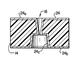
Turning next to FIG. lD, the base portion 14
is then metallized, for example, using a
conventional deposition process, so that the entire
top and bottom side surfaces 14a, 14b and the
exposed interior surfaces 15, 22, 23 which define
the first and second aperture portions 18a, 18b are
covered with a thin layer 24 of a conductive
material, for example, metal. As illustrated in
FIG. lD, the conductive layer 24 includes a first
portion 24a which covers the top side surface 14a,
a second portion 24b which covers the bottom side
surface 14b and a third portion 24c which covers
the exposed interior surfaces 15, 22 and 23.
Turning next to FIG. lE, the entire layer 24b
of conductive material deposited on the bottom side
surface 14b and part of the layer 24a of conductive
material deposited on the top side surface 14a are
then stripped away, for example, using a patterning
21 63258
-12-
process. As illustrated in FIG. lA, only a series
of longitudinal strips 16 of conductive material
remain on the top side surface 14a of the base
portion 14 after removal of a significant part of
the layer 24a. Preferably, the strips 16 are
formed to have a width slightly less than the width
of sidewall actuators 39 to be formed on top of and
conductively mounted to the strips 16 in a manner
more fully described below. A conductive pin 20 is
then insertably mounted in each of the second
aperture portions 18b of the apertures 18, for
example, using a soldering process, such that each
pin 20 engages the inner surface 15 of one of the
apertures 18, thereby electrically connecting the
pin 20 to a corresponding strip 16 of conductive
material by the portion 24c of the conductive layer
24 deposited on the inner surfaces 15, 22 and 23
which define the aperture 18.
Rather than being stripped away in the
patterning process detailed above, in an alternate
embodiment of the invention, it is contemplated
that the portion 24a of the layer 24 of conductive
material deposited on the top side surface 14a of
the lower body portion may initially be left
intact. In this embodiment, however, isolation of
the electrical connection of each pin 20 to only a
portion of the conductive material deposited on the
top side surface 14a would be achieved during
assembly of the channel array for the ink jet
printhead where, when constructing the channels of
the array, the process by which the channels are
formed would be modified such that each groove
formed during this process would extend into the
base portion 14 so that portions of the conductive
layer 24a would be removed to expose parts of the
insulative base portion 14, each of which would
-13- 21 63258
function as a bottom wall for one of the ink-
carrying channels of the array. By forming the
channels in this manner, this layer 24a of
conductive material would, in effect, be patterned
to form the series of conductive strips 16, each
electrically connected to a single pin 20.
However, such a technique would advantageously
avoid problems which may arise when attempting to
align a saw or other device used to form the
grooves in the channel array such that each groove
formed during the process is positioned between a
pair of the strips 16.
Referring next to FIGS. lA and 2-4, a method
of manufacturing a channel array 45 for an ink jet
printhead configured for interconnection with an
associated drive system from one side thereof and
constructed in accordance with the teachings of the
present invention will now be described in greater
detail. Starting with the lower body portion 10,
a first intermediate body portion 22 constructed of
an active piezoelectric material, for example, lead
zirconate titante (or "PZT"), poled in a first
direction 23 generally parallel to the lower body
portion 10, and having first and second layers 26,
28 of a conductive material, for example, metal,
mounted to top and bottom side surfaces 22a and
22b, respectively, is aligned, mated and
conductively bonded, for example, using a
conductive adhesive (not shown), for example,
conductive epoxy, such that the conductive layer 28
is conductively mounted to the conductive strips
16. Next, a second intermediate body portion 30
constructed of an active piezoelectric material,
for example, PZT, poled in a second direction 32,
opposite to the first direction 23 but also
parallel to the lower body portion 10, and having
21 63~58
-14-
first and second layers 34, 36 of a conductive
material, for example, metal, mounted to top and
bottom side surfaces 30a and 30b, respectively, is
aligned, mated and conductively bonded, again using
a conductive adhesive (not shown) such as
conductive epoxy, to the top side surface 22a of
the first intermediate body portion 22.
Referring next to FIG. 3, a series of
longitudinally extending, generally parallel
grooves 38 are formed in the channel array 45, most
commonly, using a conventional diamond sawing
process. Preferably, each groove 38 should be
formed such that it extends through the conductive
layer 34, the second intermediate body portion 30,
the conductive layer 36, the conductive layer 26,
the first intermediate body portion 22, the
conductive layer 28 and partially through the
insulative lower body portion 10 of the channel
array 45. During the forming process, the grooves
38 are precisely located such that they are formed
in between the longitudinally extending, generally
parallel strips 16 of conductive material. It
should be noted, however, that so long as a portion
of a given conductive strip 16 is in electrical
connection with the conductive layer 28, the
inadvertent removal of part of that conductive
strip 16 due to a misalignment in positioning the
saw during the forming process would not impact the
operation of the ink jet printhead 12 in any
manner.
By forming the grooves 38 in this manner, a
series of generally parallel, longitudinally
extending piezoelectric sidewall actuators 39 are
formed, preferably in a manner such that one of
conductive strips 16 runs lengthwise along the
longitudinal extension of one of the sidewall
2~ 63258
~- -15-
actuators 39 and is of a slightly lesser width than
the actuator 39. It is noted that, if the grooves
38 are precisely located between the conductive
strips 16, the grooves need only to extend through
the conductive layer 28 and need not extend into
part of the lower body portion 14 to ensure
electrical isolation of each strip 16. In any
event, it is strongly recommended that the grooves
38 are formed such that they extend into the lower
body portion 14 for both ease of manufacture and to
ensure electrical isolation of the strips in the
event of a minor misalignment during the sawing
process. Additionally, in the embodiment of the
invention where the conductive layer 24a is not
patterned into the plurality of longitudinally
extending, generally parallel strips 16, the
grooves 38 must extend through the conductive layer
24a and into the lower body portion 14 to form
electrically isolated strips 16 of conductive
material, each electrically connected to a single
sidewall actuator 39.
Referring next to FIG. 4, an upper body
portion 40 constructed of an insulative material
and having top and bottom side surfaces 40a and 40b
is aligned, mated and conductively bonded, for
example, using a conductive adhesive (not shown)
such as conductive epoxy, to the top side surface
30a of the second intermediate body portion 30 such
that a layer 42 of conductive material, for
example, metal, formed on the bottom side surface
40b of the upper body portion 40 is conductively
mounted to the layer 34 of conductive material
formed on the top side surface 30a of the second
intermediate body portion 30. In this manner, a
plurality of longitudinally extending, generally
parallel ink-carrying channels 44, each defined by
21 63258
_
-16-
part of the lower body portion 14, a first sidewall
actuator 39 comprised of a section 19 of the first
intermediate body portion 22 and a section 21 of a
second intermediate body portion 30, part of the
upper body portion 40 and a second sidewall
actuator 39, similarly comprised of a section 19 of
the first intermediate body portion 22 and a
section 21 of the second intermediate body portion
22, are formed. The assembly of a channel array 45
for an ink jet printhead 12 interconnectable to an
associated drive system from one side thereof is
now complete.
Referring next to FIG. 5, a fully assembled
ink jet printhead 12 which incorporates the channel
array 45 may now be seen. To supply ink to the
ink-carrying channels 44 of the channel array 45,
an external manifold 47 is mounted onto the ink jet
printhead such that a rear portion (shown in
phantom) of the ink jet printhead 12 is received in
an interior portion 49 thereof. The manifold 47
has a laterally extending interior channel 51
formed along the interior portion 49 thereof such
that the interior channel 51 is in communication
with the open rear ends of the ink-carrying
channels 44. An internal vertical conduit 53
having one end in communication with the internal
channel 51 is formed in the external manifold 47.
The internal conduit 53 is then connected to an
external ink conduit 46 to provide means for
supplying ink to the ink-carrying channels 44 from
a source of ink 48 connected to the external
conduit 46. A back side surface 50a of an orifice
plate 50 is then mounted to a front side surface
45a of the channel array 45 such that each orifice
52 extending through the orifice plate 50 is in
communication with a corresponding one of the ink-
21 63258
-17-
carrying channels 44 such that, when a channel 44
is compressed by application of a voltage to a
sidewall actuator 39 partially defining the channel
44, a droplet of ink will be ejected out of the
orifice 52 in communication with the compressed
channel 44 shortly thereafter and additional ink
from the ink supply 48 will be drawn into the
channel 44 from which the ink droplet had been
ejected therefrom via the external conduit 46, the
internal conduit 53 and the interior channel 51.
As should be clearly appreciated by those
skilled in the art, in comparison to prior ink jet
printheads, the electrical connection of the ink
jet printhead 12 has been tremendously simplified.
To electrically connect the ink jet printhead 12,
the layer of conductive material 42 should be
electrically connected to ground, as schematically
illustrated in FIG. 5, and each pin 20, which, as
more fully described below, controls the actuation
of a sidewall actuator 39, is electrically
connected to a driver capable of selectively
applying a positive or negative voltage to the pin
20. For example, a driver board 46 having a
plurality of pin-receiving apertures (not shown)
for receiving the pins 20 may be snap-mounted onto
the bottom side surface 14b of the channel array
45. Preferably, the driver board 46 should include
a controller for issuing control signals to actuate
selected ones of the sidewall actuators 39 and a
series of switching structures capable of
generating a positive or negative voltage at an
output thereof in response to instructions issued
by the controller. When the driver board 46 is
snap-mounted onto the channel array 45, each output
of a switching structure should become electrically
connected with one of the pins 20. Thus, a snap-in
21 63258
-18-
driver board 46 may be used to provide a separate
electrical connection to every sidewall actuator 39
for the ink jet printhead 12.
As should be further appreciated by those
skilled in the art, in comparison to prior ink jet
printheads, considerable flexibility has been added
to the interconnection of the ink jet printhead 12
and the ink supply 48. In prior ink jet
printheads, electrical interconnection between the
ink jet printhead and its controller was made at
the rear of the printhead. For this reason, it was
previously recommended that the manifold and
internal ink conduit necessary for ink to be
supplied to all of the ink-carrying channels. By
providing an ink jet printhead 12 interconnectable
from one side, either top or bottom, thereof, the
rear portion of the ink jet printhead is now
available for other uses such as the rear mounted
manifold 47 described herein.
Referring next to FIG. 6A, ink-carrying
channels 44a-44f and the portions of the channel
array 45 which define the channels 44a-f may now be
seen in greater detail. For example, the ink-
carrying channel 44c is defined by a first,
longitudinally extending sidewall actuator 39-1
formed by first intermediate portion 22-1 and
second intermediate portion 30-1, part of the upper
body portion 40, a second sidewall actuator 39-2
formed by first intermediate portion 22-2 and
second intermediate portion 30-2 and part of the
lower body portion 14. It should be noted that,
while the conductive strips 16 have a slightly
lesser width than the sidewall actuators 39, for
ease of illustration, FIGS 6A-C illustrate the two
has having equal widths.
Referring next to FIG. 6B, the ejection of a
- 21 632~8
--19--
droplet of ink from the channel 44c which is caused
by deflecting the first sidewall actuator 39-1 and
the second sidewall actuator 39-2 into the channel
44c will now be described in greater detail. To
deflect the first sidewall actuator 39-1 into the
channel 44c, a positive voltage is applied to the
conductive strip 16-l by the associated drive
system using the via 18 electrically connected
therewith, thereby creating a voltage drop across
the intermediate body portions 22-1, 30-1 and
ground (conductive layer 42). Because the first
intermediate body portion 22-1 is poled in a first
direction 23 generally orthogonal to the voltage
drop and the second intermediate body portion 30-1
is poled in a second direction 32, opposite to the
first direction 23, but also orthogonal to the
voltage drop, both the first and second
intermediate portions 22-1 and 30-1 will, as
illustrated in FIG. 6B, deflect into the channel in
shear mode.
Simultaneous with the application of a
positive voltage to the conductive strip 16-1, a
negative voltage of equal magnitude is applied to
the conductive strip 16-2, again using the via 18
connected therewith, to create a voltage drop
between ground (conductive layer 42) and the
conductive strip 16-2 which is orthogonal to the
first and second poling directions 23, 32 of the
first and second intermediate body portions 22-2
and 30-2. By reversing the direction of the
voltage drop while maintaining the same poling
directions 23, 32, the first and second
intermediate body portions 22-2 and 30-2 will now
deflect in the opposite direction which, as
illustrated in FIG. 6B, is again into the channel
44c. Of course, the first and second intermediate
21 63258
-20-
portions 22-1 and 30-1 may be deflected into the
channel 44b and the first and second intermediate
portions 22-2 and 30-2 may be deflected into the
channel 44d by applying negative and positive
voltages, respectively, at the conductive strips
16-1 and 16-2. For example, suitable positive and
negative voltages to cause the deflection of a
sidewall actuator 39 into an ink-carrying channel
44 are +40 and -40 volts.
Referring next to FIG. 6C, an alternate
configuration of the sidewall actuators 39-1 and
39-2 which increases the extent of deflection into
the channel 44c by the sidewall actuators 39-1 and
39-2, respectively, may now be seen. In this
configuration, a top side 54a of conductive spacers
54 is conductively mounted to conductive layer 36
and a bottom side 54b of the conductive spacers 54
is conductively mounted to the conductive layer 26.
Referring next to FIG. 6D, an alternate
embodiment of a bottom side surface
interconnectable ink jet printhead will now be
described in greater detail. Here, a series of
intermediate sidewall portions 57, each formed of
an active piezoelectric material poled in the
direction of arrow 59, are mounted by adhesive
layer 61 to projections 63 of inactive lower body
portion 65. A layer 67 of conductive material is
then applied to inner surfaces 69 which define the
side and bottom walls of channels 71. Assembly of
the channel array is then completed by mounting
upper body portion 73 to upper side surfaces 75 of
the active intermediate sidewall portions 57.
Shear mode deflection of the intermediate sidewall
portions 57 into the channels 71 require the
application of voltage to selected ones of the
conductive layers 67. Vias 18, which are again
-21- 2 1 632~8
formed in the lower body portion 65 in the manner
previously described are used to apply voltage to
the selected conductive layers 67. In this
embodiment, however, the vias 18 provide an
electrical connection to the channels 71 rather
than the sidewalls as set forth in the previously
described embodiments of the invention illustrated
in FIGS. 6A-C.
Referring next to FIG. 6E, yet another
alternate embodiment of a bottom side surface
interconnectable ink jet printhead will now be
described in greater detail. Here, a series of
ink-carrying channels 144 are defined by a lower
body portion 114 having a series of longitudinally
extending, generally parallel projections 122,
longitudinally extending, generally parallel
intermediate portions 130, and part of the upper
body portion 140. The intermediate portions 130
are formed of an active material poled in direction
132. This embodiment differs from that illustrated
in FIGS. 6A-B only in that the first intermediate
portions 22 illustrated in FIG. 6A have been
removed and the channels 144 now extend into the
lower body portion 114. Accordingly, in this
embodiment, the sidewalls 139 are comprised of the
inactive projections 122 of the lower body portion
114 and the active intermediate body portions 130
which, upon application of a voltage thereto, will
deflect into the channels 144 in a shear motion.
In this embodiment, therefore, the vias 18 should
be extended to the conductive layers 116 so that
sidewall deflecting voltages may be applied
directly to the intermediate body portions 130.
Referring next to FIG. 7, an alternate
embodiment of a channel array 56 suitable for
interconnection with an associated drive system
~_ 21 63258
-22-
from one side thereof, which, in this embodiment of
the invention, is the top side, may now be seen.
In this embodiment, a lower body portion 58
constructed of an active piezoelectric material
poled in a first direction 62 and having a layer 60
of conductive material formed on a top side surface
thereof is first provided. A bottom side surface
of an intermediate body portion 64 having first and
second layers 66, 68 of conductive material
respectively formed on the top and bottom side
surfaces thereof, is then conductively mounted to
the top side surface of the lower body portion 58.
The intermediate body portion 64 is formed of an
active piezoelectric material poled in a second
direction 70 oppositely orientated to, but parallel
with the first direction 62.
After mounting the lower and intermediate body
portions 58, 64 together, a series of generally
parallel, longitudinally extending grooves which
extend through the entire intermediate body portion
64 and part of the lower body portion 58 are
formed, for example, by a sawing process. A bottom
side surface of an upper body portion 72, similar
in design but inverted in orientation to the lower
body portion 10 of FIG. lA is then conductively
mounted onto the layer 66 of conductive material.
The upper body portion is formed of an insulative
material and has a plurality of generally parallel,
longitudinally extending conductive strips 74
(shown in phantom in FIG. 7) formed on the bottom
side surface thereof. Each conductive strip 74 is
electrically connected to the conductive layer 66
and to a via 78 which extends through the upper
body portion 72 and to the top side surface 72a
where interconnection with an associated drive
system may be easily achieved.
-
21 63258
-23-
By forming the channel array 56 in this
manner, a plurality of ink-carrying channels 76,
each defined by a first intermediate body portion
64, part of the lower body portion 58, a second
intermediate body portion 64 and part of the upper
body portion 72 are formed. Each ink-carrying
channel 76 has first, second and third actuators
associated therewith--the first and second
intermediate body portions 64 and a generally U-
shaped part 82 of the lower body portion 58 which
defines a portion of the channel 76. To actuate an
ink-carrying channel 76, for example, the channel
76-1, a positive voltage is applied to a first via
78-1 electrically connected to a first sidewall 80-
1 which partially defines the channel 76-1 and a
negative voltage is applied to a second via 78-2
electrically connected to a second sidewall 80-2
which partially defines the channel 76-1. This
creates a voltage drop from the conductive layer
66-1 to the conductive layer 66-2 which causes the
intermediate body portion 66-1, the arms 84 of the
generally U-shaped part 82 of the lower body
portion 14 and the intermediate body portion 66-2
to all deflect into the channel 76-1 to impart an
ink ejecting compressive pressure pulse thereto.
For example, suitable positive and negative
voltages to cause the deflection of the first and
second intermediate body portions 64 and the arms
84 of the U-shaped part 82 of the lower body
portion 58 into an ink-carrying channel 76 are +80
and -80 volts.
Referring next to FIG. 8, a second embodiment
of a top side surface drive system interconnectable
channel array 86 for an ink jet printhead may now
be seen. In this embodiment, an insulative base
portion 88 having a layer 90 of conductive material
21 63258
-24-
formed on a top side surface thereof and a first
intermediate body portion 92 formed from an active
piezoelectric material poled in direction 94a and
having layers 96 and 98 of conductive material
respectively formed on top and bottom side surfaces
thereof are now provided. The conductive layer 98
of the first intermediate body portion 92 is
conductively mounted to the conductive layer 90 of
the lower body portion 88. As schematically
illustrated in FIG. 8, the conductive layer 90 is
also connected to ground.
A second intermediate body portion 100 formed
from an active piezoelectric material poled in
direction 94b and having layers 102 and 104 of
conductive material respectively formed on the top
and bottom sides thereof is then conductively
mounted to the first intermediate body portion 92
by conductively mounting the layers 96 and 104 to
each other. A series of generally parallel,
longitudinally extending grooves which extend
through the second and first intermediate body
portions 100 and 92 to expose the conductive layer
are then formed, for example, by a sawing
process. An upper body portion 72 identical to
that illustrated in FIG. 7 is then conductively
mounted to the conductive layer 102, thereby
forming a plurality of ink-carrying channels 106,
each defined by part of the lower body portion 88,
a pair of first intermediate body portions 92, a
pair of second intermediate body portions 100 and
a part of the upper body portion 72.
To actuate an ink-carrying channel, for
example, ink-carrying channel 106-1, a positive
voltage is applied by an associated drive system to
the conductive layer 102-1 and a negative voltage
is applied by the drive system to the conductive
-25- 2 t 632~8
layer 102-2. By doing so, first and second voltage
drops generally orthogonal to the poling direction
94 are formed between the conductive layers 102-1,
102-2, respectively, and ground (the conductive
layer 90), thereby causing the deflection of all
four active intermediate body portions 92-1, 92-2,
100-1 and 100-2 into the channel 106-1 to impart an
ink ejection initiating compressive pressure pulse
into the channel 106-1. For example, suitable
positive and negative voltages to cause the
deflection of the intermediate body portions 92-1,
92-2, 100-1 and 100-2 into the channel 106-1 are
+40 and -40 volts.
Thus, there has been described and illustrated
herein, an ink jet printhead which is
interconnectable with an associated drive system
from one side thereof. However, those skilled in
the art will recognize that many modifications and
variations besides those specifically mentioned may
be made in the techniques described herein without
departing substantially from the concept of the
present invention. Accordingly, it should be
clearly understood that the form of the invention
as described herein is exemplary only and is not
intended as a limitation on the scope of the
invention.